


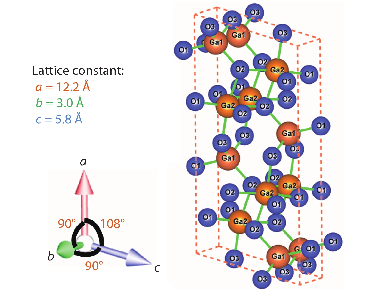
Fig. 1.
(Color online) Atomic unit cell of β-Ga2O3 with lattice constant and angle marked.
REVIEWS
Hong Zhou, Jincheng Zhang, Chunfu Zhang, Qian Feng, Shenglei Zhao, Peijun Ma and Yue Hao
Corresponding author: Jincheng Zhang, jchzhang@xidian.edu.cn
Abstract: Until very recently, gallium oxide (Ga2O3) has aroused more and more interests in the area of power electronics due to its ultra-wide bandgap of 4.5–4.8 eV, estimated critical field of 8 MV/cm and decent intrinsic electron mobility limit of 250 cm2/(V·s), yielding a high Baliga’s figures-of-merit (FOM) of more than 3000, which is several times higher than GaN and SiC. In addition to its excellent material properties, potential low-cost and large size substrate through melt-grown methodology also endows β-Ga2O3 more potential for future low-cost power devices. This article focuses on reviewing the most recent advances of β-Ga2O3 based power devices. It will be starting with a brief introduction to the material properties of β-Ga2O3 and then the growth techniques of its native substrate, followed by the thin film epitaxial growth. The performance of state-of-art β-Ga2O3 devices, including diodes and FETs are fully discussed and compared. Finally, potential solutions to the challenges of β-Ga2O3 are also discussed and explored.
Keywords: gallium oxide, power electronics, power devices
| [1] |
Zhang Y, Joishi C, Xia Z et al. Demonstration of β-(AlxGa1-x)2O3/Ga2O3 double heterostructure field effect transistors. Appl Phys Lett 2018, 112: 233503 doi: 10.1063/1.5037095
|
| [2] |
Lv Y, Zhou X, Long S et al. Source-Field-Plated β-Ga2O3 MOSFET with Record Power Figure of Merit of 50.4 MW/cm2. IEEE Electron Device Lett 2019, 39 doi: 10.1109/LED.2018.2881274
|
| [3] |
Green A J, Chabak K, Heller E R, et al. 3.8 MV/cm Breakdown strength of MOVPE-grown Sn-doped Ga2O3 MOSFETs. IEEE Electron Device Lett, 2016, 37 (7): 902. doi: 10.1109/LED.2016.2568139
|
| [4] |
Chabak K D, Moser N, Green A J, et al. Enhancement-mode Ga2O3 wrap-gate fin field-effect transistors on native (100) β-Ga2O3 substrate with high breakdown voltage. Appl Phys Lett, 2016, 109: 213501. doi: 10.1063/1.4967931
|
| [5] |
Tadjer M, Mahadik N, Wheeler V D, et al. Communications-A (001) β-Ga2O3 MOSFETs with +2.9 V threshold voltage and HfO2 gate dielectric. ECS J Solid State Sci Tech, 2016, 5: 468. doi: 10.1149/2.0061609jss
|
| [6] |
Zeng K, Wallace J S, Heimburger C, et al. Ga2O3 MOSFETs using spin-on-glass source/drain doping technology. IEEE Electron Device Lett, 2017, 38 (4): 513. doi: 10.1109/LED.2017.2675544
|
| [7] |
Wort C J H, Balmer R S. Diamond as an electronic material. Mater Today, 2008, 11 (1): 22. doi: 10.1016/S1369-7021(07)70349-8
|
| [8] |
Fu H, Baranowski I, Huang X, et al. Demonstration of AlN Schottky barrier diodes with blocking voltage over 1 kV. IEEE Electron Device Lett, 2017, 38 (9): 1286. doi: 10.1109/LED.2017.2723603
|
| [9] |
Baliga B J. Power semiconductor-device figure of merit for high-frequency applications. IEEE Electron Device Lett, 1989, 10(10): 455. doi: 10.1109/55.43098
|
| [10] |
Wenckstern H V. Group‐III sesquioxides: growth, physical properties and devices. Adv Electron Mater, 2017, 3(9): 1600350. doi: 10.1002/aelm.v3.9
|
| [11] |
Yoshioka S, Hayashi H, Kuwabara A, et al. Structures and energetics of Ga2O3 polymorphs. J Phys: Condens Matter, 2007, 19: 346211. doi: 10.1088/0953-8984/19/34/346211
|
| [12] |
He H, Orlando R, Blanco M A, et al. First-principles study of the structural, electronic, and optical properties of Ga2O3 in its monoclinic and hexagonal phases. Phys Rev B, 2006, 74 (19): 195123. doi: 10.1103/PhysRevB.74.195123
|
| [13] |
He H, Blanco M A, Pandey R. Electronic and thermodynamic properties of Ga2O3. Appl Phys Lett, 2006, 88: 261904. doi: 10.1063/1.2218046
|
| [14] |
Kroll P, Dronskowski R, Martin M. Formation of spinel-type gallium oxynitrides: a density-functional study of binary and ternary phases in the system Ga–O–N. J Mater Chem, 2005, 15: 3296. doi: 10.1039/b506687e
|
| [15] |
Playford H Y, Hannon A C, Barney E R, et al. Structures of Uncharacterised Polymorphs of Gallium Oxide from Total Neutron Diffraction. Eur J, 2013, 19 (8): 2803. doi: 10.1002/chem.201203359
|
| [16] |
Peelaers H, Van de Walle C G. Brillouin zone and band structure of β‐Ga2O3. Phys Status Solidi B, 2015, 252 (4): 828. doi: 10.1002/pssb.201451551
|
| [17] |
Varley J B, Weber J R, Janotti A, et al. Oxygen vacancies and donor impurities in β-Ga2O3. Appl Phys Lett, 2010, 97: 142106. doi: 10.1063/1.3499306
|
| [18] |
Vasyltsiv V I, Rym Y I, Zakharo Y M. Optical absorption and photoconductivity at the band edge of β‐Ga2−xInxO3. Phys Status Solidi B, 1996, 195, 653. doi: 10.1002/(ISSN)1521-3951
|
| [19] |
Galazka Z, Irmscher K, Uecker R, et al. On the bulk β-Ga2O3 single crystals grown by the Czochralski method. J Cryst Growth, 2014, 404 (15): 184. doi: 10.1016/j.jcrysgro.2014.07.021
|
| [20] |
Galazka Z, Uecker R, Irmscher K, et al. Czochralski growth and characterization of β‐Ga2O3 single crystals. Cryst Res Technol, 2010, 45 (12), 1229. doi: 10.1002/crat.v45.12
|
| [21] |
Kuramata A, Koshi K, Watanabe S, et al. High-quality β-Ga2O3 single crystals grown by edge-defined film-fed growth. Jpn J App Phys Part 1, 2016, 55, 1202A2. doi: 10.7567/JJAP.55.1202A2
|
| [22] |
Vıllora E G, Morioka Y, Atou T. Infrared reflectance and electrical conductivity of β-Ga2O3. Phys. Status Solidi A, 2002, 193: 187. doi: 10.1002/(ISSN)1521-396X
|
| [23] |
Zhang J, Li B, Xia C, Growth and spectral characterization of β-Ga2O3 single crystals. J Phys Chem Solids, 2006, 67: 2448. doi: 10.1016/j.jpcs.2006.06.025
|
| [24] |
Suzuki N, Ohira S, Tanaka M. Fabrication and characterization of transparent conductive Sn-doped β-Ga2O3 single crystal. Phys Status Solidi C, 2007, 4 (7): 2310. doi: 10.1002/(ISSN)1610-1642
|
| [25] |
Mohamed M, Irmscher K, Janowitz C, et al. Schottky barrier height of Au on the transparent semiconducting oxide β-Ga2O3. Appl Phys Lett, 2012, 101: 132106. doi: 10.1063/1.4755770
|
| [26] |
Suzuki K, Okamoto T, Takata M. Crystal growth of β-Ga2O3 by electric current heating method. Ceram Int, 2004, 30(7): 1679. doi: 10.1016/j.ceramint.2003.12.154
|
| [27] |
Zhang J, Xia C, Deng Q, et al. Growth and characterization of new transparent conductive oxides single crystals β-Ga2O3: Sn. J Phys Chem Solids, 2006, 67: 1656. doi: 10.1016/j.jpcs.2006.02.018
|
| [28] |
Tomm Y, Reiche P, Klimm D, et al. Czochralski grown Ga2O3 crystals. J Cryst Growth, 2000, 220 (4): 510. doi: 10.1016/S0022-0248(00)00851-4
|
| [29] |
Galazka Z, Uecker R, Klimm D et al.Scaling-Up of Bulk β-Ga2O3 Single Crystals by the Czochralski Method. ECS J Solid State Sci Technol 2017, 6: Q3007 doi: 10.1016/j.jcrysgro.2014.07.021
|
| [30] |
Higashiwaki M, Kuramata A, Murakami H, et al. State-of-the-art technologies of gallium oxide power devices. J Phys D, 2017, 50: 333002. doi: 10.1088/1361-6463/aa7aff
|
| [31] |
Hoshikawa K, Ohba E, Kobayashi E, et al. Growth of β-Ga2O3 single crystals using vertical Bridgman method in ambient air. J Cryst Growth, 2016, 447 (1): 36. doi: 10.1016/j.jcrysgro.2016.04.022
|
| [32] |
Alema F, Hertog B, Osinsky A, et al. Fast growth rate of epitaxial β–Ga2O3 by close coupled showerhead MOCVD. J Cryst Growth, 2017, 475: 77. doi: 10.1016/j.jcrysgro.2017.06.001
|
| [33] |
Gogova D, Wagner G, Baldini M, et al. Structural properties of Si-doped β-Ga2O3 layers grown by MOVPE. J Cryst Growth, 2014, 401: 665. doi: 10.1016/j.jcrysgro.2013.11.056
|
| [34] |
Baldini M, Albrecht M, Fiedler A, et al. Semiconducting Sn-doped β-Ga2O3 homoepitaxial layers grown by metal organic vapour-phase epitaxy. J Mater Sci, 2016, 51(7): 3650. doi: 10.1007/s10853-015-9693-6
|
| [35] |
Sasaki K, Higashiwaki M, Kuramata A, et al. Growth temperature dependences of structural and electrical properties of Ga2O3 epitaxial films grown on β-Ga2O3 (010) substrates by molecular beam epitaxy. J Cryst Growth, 2014, 392: 30. doi: 10.1016/j.jcrysgro.2014.02.002
|
| [36] |
Oshima T, Okuno T, Fujita S. Ga2O3 thin film growth on c-plane sapphire substrates by molecular beam epitaxy for deep-ultraviolet photodetectors. Jpn J Appl Phys, 2007, 46: 7217. doi: 10.1143/JJAP.46.7217
|
| [37] |
Okumura H, Kita M, Sasaki K, et al. Systematic investigation of the growth rate of β-Ga2O3(010) by plasma-assisted molecular beam epitaxy. Appl Phys Express, 2014, 7: 095501. doi: 10.7567/APEX.7.095501
|
| [38] |
Oshima T, Arai N, Suzuki N, et al. Surface morphology of homoepitaxial β-Ga2O3 thin films grown by molecular beam epitaxy. Thin Solid Films, 2008, 516: 5768. doi: 10.1016/j.tsf.2007.10.045
|
| [39] |
Y Oshima, E G Vıllora, K Shimamura. Halide vapor phase epitaxy of twin-free α-Ga2O3 on sapphire (0001) substrates. Appl Phys Express, 2015, 8: 055501. doi: 10.7567/APEX.8.055501
|
| [40] |
Watahiki T, Yuda Y, Furukawa A, et al. Heterojunction p-Cu2O/n-Ga2O3 diode with high breakdown voltage. Appl Phys Lett, 2017, 111: 222104. doi: 10.1063/1.4998311
|
| [41] |
Murakami H, Nomura K, Goto K, et al. Homoepitaxial growth of β-Ga2O3 layers by halide vapor phase epitaxy. Appl Phys Express, 2015, 8: 015503. doi: 10.7567/APEX.8.015503
|
| [42] |
K Nomura, K Goto, R Togashi, et al. Thermodynamic study of β-Ga2O3 growth by halide vapor phase epitaxy. J Cryst Growth, 2014, 405: 19. doi: 10.1016/j.jcrysgro.2014.06.051
|
| [43] |
Hebert C, Petitmangin A, Perrie're J, et al. Phase separation in oxygen deficient gallium oxide films grown by pulsed-laser deposition. Mater Chem Phys, 2012, 133 (1): 135. doi: 10.1016/j.matchemphys.2011.12.078
|
| [44] |
Chen Z, Wang X, Noda S, et al. Effects of dopant contents on structural, morphological and optical properties of Er doped Ga2O3 films. Superlattices Microstruct, 2016, 90: 207. doi: 10.1016/j.spmi.2015.12.025
|
| [45] |
Kawaharamura T. Physics on development of open-air atmospheric pressure thin film fabrication technique using mist droplets: Control of precursor flow. Jpn J Appl Phys, 2014, 53: 05FF08. doi: 10.7567/JJAP.53.05FF08
|
| [46] |
Lee S D, Kaneko K, Fujita S. Homoepitaxial growth of beta gallium oxide films by mist chemical vapor deposition. Jpn J Appl Phys, 2016, 55: 1202B8. doi: 10.7567/JJAP.55.1202B8
|
| [47] |
Dang G T, Kawaharamura T, Furuta M, et al. Metal–semiconductor field-effect transistors with In–Ga–Zn–O channel grown by nonvacuum-processed mist chemical vapor deposition. IEEE Electron Device Lett, 2015, 36 (5): 463. doi: 10.1109/LED.2015.2412124
|
| [48] |
Fujita S, Kaneko K. Epitaxial growth of corundum-structured wide band gap III-oxide semiconductor thin films. J Cryst Growth, 2014, 401: 588. doi: 10.1016/j.jcrysgro.2014.02.032
|
| [49] |
Akaiwa K, Fujita S. Electrical conductive corundum-structured α-Ga2O3 thin films on sapphire with tin-doping grown by spray-assisted mist chemical vapor deposition. Jpn J Appl Phys, 2012, 51: 070203. doi: 10.1143/JJAP.51.070203
|
| [50] |
Baldini M, Albrecht M, Gogova D, et al. Effect of indium as a surfactant in (Ga1−xInx)2O3 epitaxial growth on β-Ga2O3 by metal organic vapour phase epitaxy. Semicond Sci Technol, 2015, 30: 024013. doi: 10.1088/0268-1242/30/2/024013
|
| [51] |
Hu Z, Zhou H, Feng Q. Field-plated lateral β-Ga2O3 Schottky barrier diode with high reverse blocking voltage of more than 3 kV and high power figure-of-merit of 500 MW/cm2. IEEE Electron Device Lett, 2018, 39(10): 1564. doi: 10.1109/LED.2018.2868444
|
| [52] |
Sasaki K, Kuramata A, Masui T, et al. Device-quality beta-Ga2O3 epitaxial films fabricated by ozone molecular beam epitaxy. Appl Phys Exp, 2012, 5: 035502. doi: 10.1143/APEX.5.035502
|
| [53] |
Konishi K, Goto K, Murakami H, et al. 1-kV vertical β-Ga2O3 field-plated Schottky barrier diodes. Appl Phys Lett, 2017, 110 (10): 103506. doi: 10.1063/1.4977857
|
| [54] |
Yang J, Ahn S, Ren F, et al. High reverse breakdown voltage Schottky rectifiers without edge termination on β-Ga2O3. Appl Phys Lett, 2017, 110 (19): 192101. doi: 10.1063/1.4983203
|
| [55] |
Yang J, Ahn S, Ren F, et al. High breakdown voltage (−201) β-Ga2O3 Schottky rectifiers. IEEE Electron Device Lett, 2017, 38 (7): 906. doi: 10.1109/LED.2017.2703609
|
| [56] |
Yang J, Ren F, Pearton S J, et al. Vertical geometry 2-A forward current Ga2O3 Schottky rectifiers on bulk Ga2O3 substrates. IEEE Trans Electron Devices, 2018, 65(7): 2790. doi: 10.1109/TED.2018.2838439
|
| [57] |
Higashiwaki M, Sasaki K, Kuramata A, et al. Gallium oxide (Ga2O3) metal−semiconductor field-effect transistors on single-crystal β-Ga2O3 (010) substrates. Appl Phys Lett 2012, 100: 013504. doi: 10.1063/1.3674287
|
| [58] |
Wong M H, Sasaki K, Kuramata A, et al. Field-plated Ga2O3 MOSFETs with a breakdown voltage of over 750 V. IEEE Electron Device Lett, 2016, 37: 212. doi: 10.1109/LED.2015.2512279
|
| [59] |
Zeng K, Vaidya A, Singisetti U, et al. 1.85 kV breakdown voltage in lateral field-plated Ga2O3 MOSFETs. IEEE Electron Device Lett, 2018, 39(9): 1385. doi: 10.1109/LED.2018.2859049
|
| [60] |
Zeng K, Sasaki K, Kuramata A, et al. Depletion and enhancement mode β-Ga2O3 MOSFETs with ALD SiO2 gate and near 400 V breakdown voltage. Proc 74th Annu DRC, 2016: 1
|
| [61] |
Hu Z, Nomoto K, Li W, et al. Enhancement-mode Ga2O3 vertical transistors with breakdown voltage >1 kV. IEEE Electron Device Lett, 2018, 39(6): 869. doi: 10.1109/LED.2018.2830184
|
| [62] |
Green A J, Chabak K D, Baldini M, et al. β-Ga2O3 MOSFETs for radio frequency operation. IEEE Electron Device Lett, 2017.38 (6): 790. doi: 10.1109/LED.2017.2694805
|
| [63] |
Singh M, Casbon M A, Uren M J, et al. Pulsed large signal rf performance of field-plated Ga2O3 MOSFETs. IEEE Electron Device Lett, 2018.39 (10): 1572. doi: 10.1109/led.2018.2865832
|
| [64] |
Chabak K D, Walker D E, Green A J, et al. sub-micron gallium oxide radio frequency field-effect transistors. IEEE MTT-S IMWS-AMP, 2018: 1
|
| [65] |
Hwang W S, Verma A, Peelaers H, et al. High-voltage field effect transistors with wide-bandgap beta-Ga2O3 nanomembranes. Appl Phys Lett, 2014, 104: 203111. doi: 10.1063/1.4879800
|
| [66] |
Hu Z, Zhou H, Dang K, et al. lateral-ga2o3 schottky barrier diode on sapphire substrate with reverse blocking voltage of 1.7 kV. IEEE J Electron Device Soc, 2018, 6: 815. doi: 10.1109/JEDS.2018.2853615
|
| [67] |
Zhou H, Maize K, Qiu G, et al. β-Ga2O3 on insulator field-effect transistors with drain currents exceeding 1.5 A/mm and their self-heating effect. Appl Phys Lett, 2017, 111: 092102. doi: 10.1063/1.5000735
|
| [68] |
: Zhou H, Si M, Alghamdi S, et al. High performance depletion/ enhancement mode β-Ga2O3 on insulator (GOOI) field-effect transistors with record drain currents of 600/450 mA/mm. IEEE Electron Device Lett, 2017, 38: 103. doi: 10.1109/LED.2016.2635579
|
| [69] |
Moser N A, Mccandless J P, Crespo A, et al. High pulsed density β-Ga2O3 MOSFETs verified by an analytical model corrected for interface charge. Appl Phys Lett, 2017, 110: 143505. doi: 10.1063/1.4979789
|
| [70] |
Shin S H, Wahab M A, Masuduzzaman A, et al. Direct observation of self-heating in III–V gate-all-around nanowire MOSFETs. IEEE Trans Electron Devices, 2014, 62: 3516. doi: 10.1109/IEDM.2014.7047088
|
| [71] |
Zhou H, Maize K, Noh J, et al. Thermo-dynamic studies of β-Ga2O3 nano-membrane field-effect transistors on sapphire substrate. ACS Omega, 2017, 2: 7723. doi: 10.1021/acsomega.7b01313
|
| [72] |
Noh J, Si M, Zhou H, et al. The impact of substrates on the performance of top-gate β-Ga2O3 field-effect transistors: record high drain current of 980 mA/mm on diamond. IEEE Device Research Conference, 2018: 1.
|
| [73] |
Maize K, Zibari A, French W D, et al. Thermoreflectance ccd imaging of self-heating in power MOSFET arrays. IEEE Trans Electron Devices 2014, 61: 3047. doi: 10.1109/TED.2014.2332466
|
| [74] |
Si M, Yang L, Zhou H, et al. β-Ga2O3 Nanomembrane negative capacitance field-effect transistors with steep subthreshold slope for wide band gap logic applications. ACS Omega, 2017, 2: 7136. doi: 10.1021/acsomega.7b01289
|


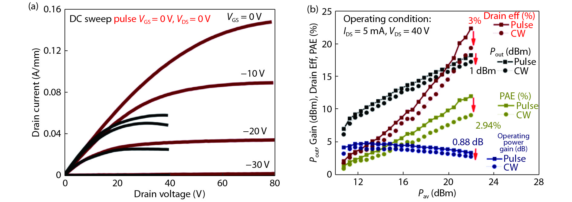
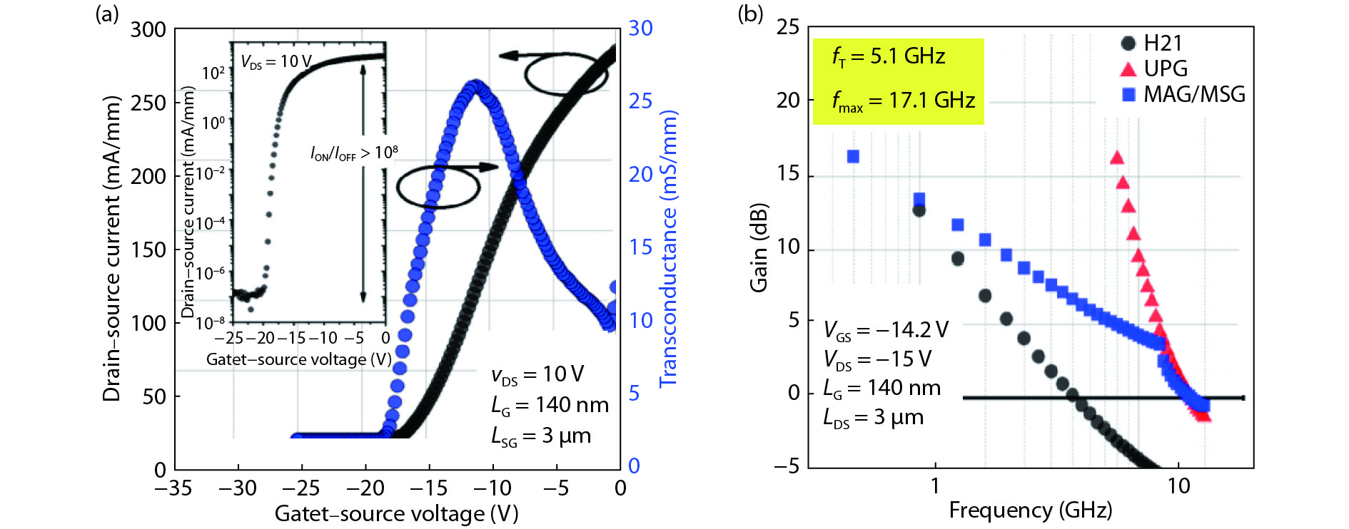
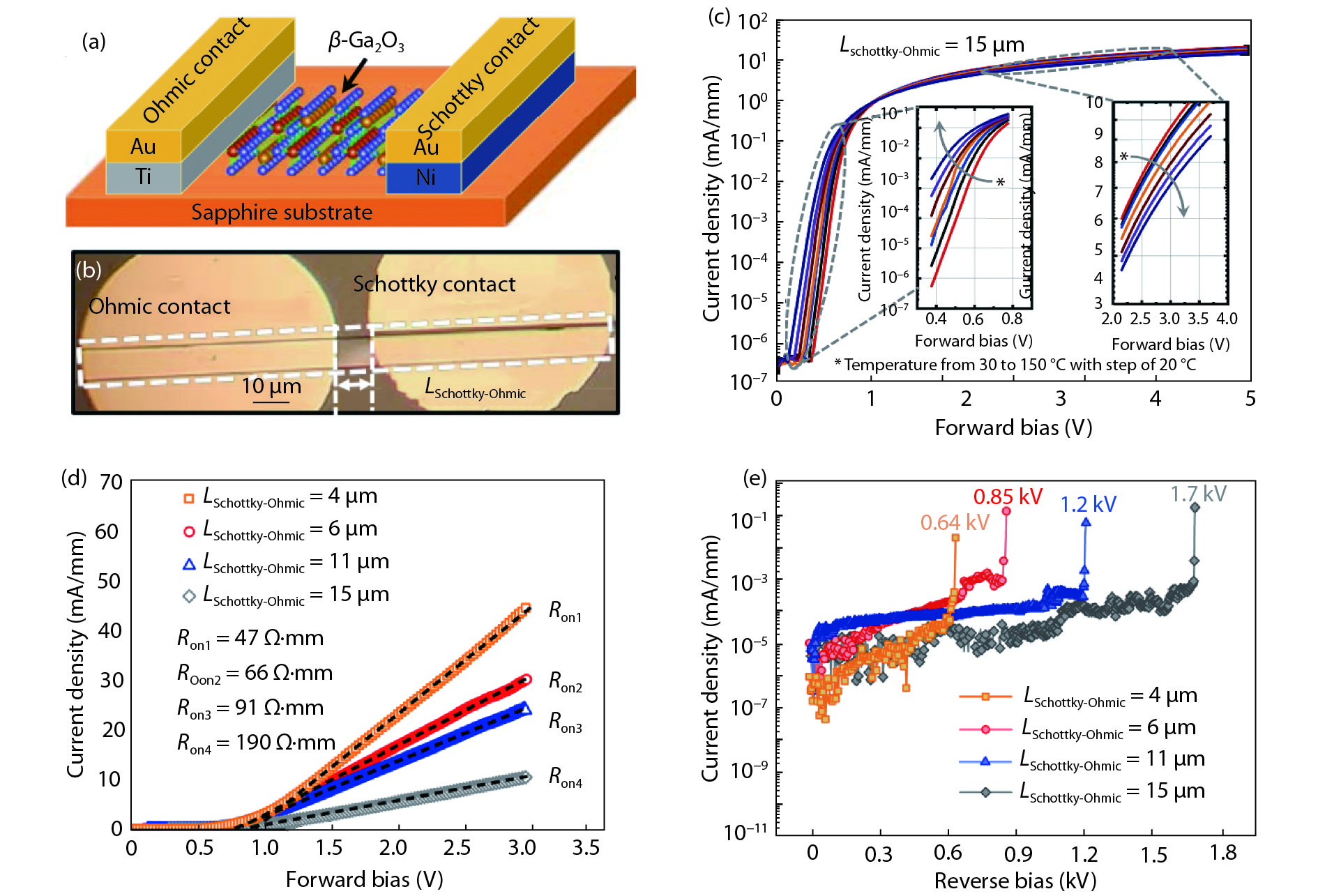

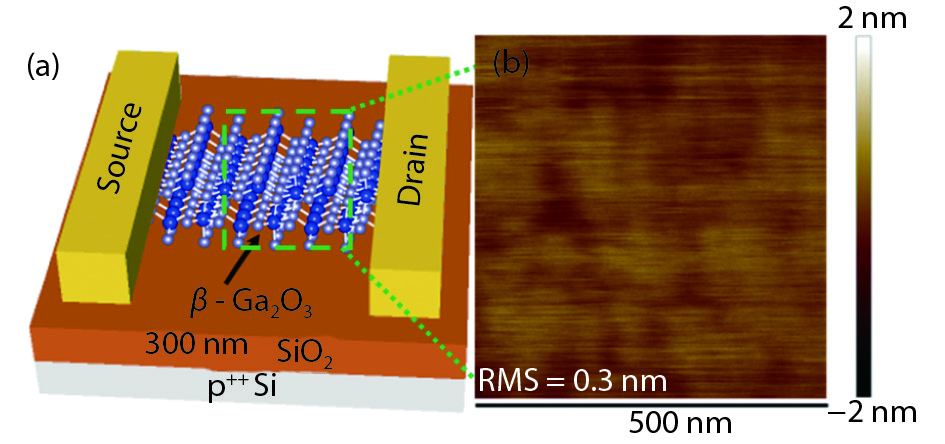


Table 1. Properties of β-Ga2O3 relative to some other major semiconductors used for power electronics applications, considering their different kinds of FOM.
| Material Parameter | Si | GaAs | 4H-SiC | GaN | Diamond | β-Ga2O3 |
| Bandgap Eg (eV) | 1.14 | 1.43 | 3.25 | 3.4 | 5.5 | 4.8 |
| Dielectric constant ε | 12 | 13 | 10 | 9 | 5.5 | 11 |
| Breakdown field EC (MV/cm) | 0.3 | 0.4 | 2.5 | 3.3 | 10 | 8 |
| Carrier mobility μ (cm2/(V·s)) | 1450 | 8400 | 1000 | 1200 | 2000 | 300 |
| Saturation velocity νsat (107 cm/s) | 1 | 1.2 | 2 | 2.5 | 1 | 2 |
| Thermal conductivity κ (W/mK) | 150 | 50 | 370 | 250 | 2000 | 10–30 |
| FOM relative to Si | ||||||
| Baliga FOM = εμEc3 | 1 | 14.7 | 317 | 846 | 24 660 | 3200 |
| Johnson FOM = Ec2νsat2/4π2 | 1 | 1.8 | 278 | 1089 | 1110 | 2844 |
| Baliga High Frequency FOM = μEc2 | 1 | 10 | 46 | 100 | 1500 | 142 |
| Keyes FOM = κ[(cνsat)(4πε)]1/2 | 1 | 0.3 | 3.6 | 1.8 | 41.5 | 0.2 |
 DownLoad: CSV
Table 2. Comparison of CW and pulse large signal measurements performed at two different operating power levels of 0.4 and 0.8 W/mm. larger differences in performance between cw and pulsed modes can been seen with increasing operating power. Reprinted from IEEE Electron Device Lett, 39, 1572, 2018. Copyright of 2018 IEEE.
| Parameter | Operating condition 0.4 W/mm 25 °C
(IDS = 5 mA, Vds = 40 V) |
Operating condition 0.8 W/mm 25 °C
(IDS = 10 mA, VDS = 40 V) |
||
| CW | Pulse | CW | Pulse | |
| Pout (dBm) | 17.42 | 18.28 | 17.63 | 19.52 |
| Pout (W/mm) | 0.11 | 0.13 | 0.11 | 0.17 |
| Drain Eff (%) | 19.56 | 22.40 | 13.83 | 17.04 |
| PAE (%) | 9.09 | 12.01 | 3.23 | 6.85 |
| Max gain (dB) | 4.17 | 4.81 | 2.08 | 3.68 |
| Channel temperature (°C) | 58 | 28 | 97 | 36 |
DownLoad: CSV
| [1] |
Zhang Y, Joishi C, Xia Z et al. Demonstration of β-(AlxGa1-x)2O3/Ga2O3 double heterostructure field effect transistors. Appl Phys Lett 2018, 112: 233503 doi: 10.1063/1.5037095
|
| [2] |
Lv Y, Zhou X, Long S et al. Source-Field-Plated β-Ga2O3 MOSFET with Record Power Figure of Merit of 50.4 MW/cm2. IEEE Electron Device Lett 2019, 39 doi: 10.1109/LED.2018.2881274
|
| [3] |
Green A J, Chabak K, Heller E R, et al. 3.8 MV/cm Breakdown strength of MOVPE-grown Sn-doped Ga2O3 MOSFETs. IEEE Electron Device Lett, 2016, 37 (7): 902. doi: 10.1109/LED.2016.2568139
|
| [4] |
Chabak K D, Moser N, Green A J, et al. Enhancement-mode Ga2O3 wrap-gate fin field-effect transistors on native (100) β-Ga2O3 substrate with high breakdown voltage. Appl Phys Lett, 2016, 109: 213501. doi: 10.1063/1.4967931
|
| [5] |
Tadjer M, Mahadik N, Wheeler V D, et al. Communications-A (001) β-Ga2O3 MOSFETs with +2.9 V threshold voltage and HfO2 gate dielectric. ECS J Solid State Sci Tech, 2016, 5: 468. doi: 10.1149/2.0061609jss
|
| [6] |
Zeng K, Wallace J S, Heimburger C, et al. Ga2O3 MOSFETs using spin-on-glass source/drain doping technology. IEEE Electron Device Lett, 2017, 38 (4): 513. doi: 10.1109/LED.2017.2675544
|
| [7] |
Wort C J H, Balmer R S. Diamond as an electronic material. Mater Today, 2008, 11 (1): 22. doi: 10.1016/S1369-7021(07)70349-8
|
| [8] |
Fu H, Baranowski I, Huang X, et al. Demonstration of AlN Schottky barrier diodes with blocking voltage over 1 kV. IEEE Electron Device Lett, 2017, 38 (9): 1286. doi: 10.1109/LED.2017.2723603
|
| [9] |
Baliga B J. Power semiconductor-device figure of merit for high-frequency applications. IEEE Electron Device Lett, 1989, 10(10): 455. doi: 10.1109/55.43098
|
| [10] |
Wenckstern H V. Group‐III sesquioxides: growth, physical properties and devices. Adv Electron Mater, 2017, 3(9): 1600350. doi: 10.1002/aelm.v3.9
|
| [11] |
Yoshioka S, Hayashi H, Kuwabara A, et al. Structures and energetics of Ga2O3 polymorphs. J Phys: Condens Matter, 2007, 19: 346211. doi: 10.1088/0953-8984/19/34/346211
|
| [12] |
He H, Orlando R, Blanco M A, et al. First-principles study of the structural, electronic, and optical properties of Ga2O3 in its monoclinic and hexagonal phases. Phys Rev B, 2006, 74 (19): 195123. doi: 10.1103/PhysRevB.74.195123
|
| [13] |
He H, Blanco M A, Pandey R. Electronic and thermodynamic properties of Ga2O3. Appl Phys Lett, 2006, 88: 261904. doi: 10.1063/1.2218046
|
| [14] |
Kroll P, Dronskowski R, Martin M. Formation of spinel-type gallium oxynitrides: a density-functional study of binary and ternary phases in the system Ga–O–N. J Mater Chem, 2005, 15: 3296. doi: 10.1039/b506687e
|
| [15] |
Playford H Y, Hannon A C, Barney E R, et al. Structures of Uncharacterised Polymorphs of Gallium Oxide from Total Neutron Diffraction. Eur J, 2013, 19 (8): 2803. doi: 10.1002/chem.201203359
|
| [16] |
Peelaers H, Van de Walle C G. Brillouin zone and band structure of β‐Ga2O3. Phys Status Solidi B, 2015, 252 (4): 828. doi: 10.1002/pssb.201451551
|
| [17] |
Varley J B, Weber J R, Janotti A, et al. Oxygen vacancies and donor impurities in β-Ga2O3. Appl Phys Lett, 2010, 97: 142106. doi: 10.1063/1.3499306
|
| [18] |
Vasyltsiv V I, Rym Y I, Zakharo Y M. Optical absorption and photoconductivity at the band edge of β‐Ga2−xInxO3. Phys Status Solidi B, 1996, 195, 653. doi: 10.1002/(ISSN)1521-3951
|
| [19] |
Galazka Z, Irmscher K, Uecker R, et al. On the bulk β-Ga2O3 single crystals grown by the Czochralski method. J Cryst Growth, 2014, 404 (15): 184. doi: 10.1016/j.jcrysgro.2014.07.021
|
| [20] |
Galazka Z, Uecker R, Irmscher K, et al. Czochralski growth and characterization of β‐Ga2O3 single crystals. Cryst Res Technol, 2010, 45 (12), 1229. doi: 10.1002/crat.v45.12
|
| [21] |
Kuramata A, Koshi K, Watanabe S, et al. High-quality β-Ga2O3 single crystals grown by edge-defined film-fed growth. Jpn J App Phys Part 1, 2016, 55, 1202A2. doi: 10.7567/JJAP.55.1202A2
|
| [22] |
Vıllora E G, Morioka Y, Atou T. Infrared reflectance and electrical conductivity of β-Ga2O3. Phys. Status Solidi A, 2002, 193: 187. doi: 10.1002/(ISSN)1521-396X
|
| [23] |
Zhang J, Li B, Xia C, Growth and spectral characterization of β-Ga2O3 single crystals. J Phys Chem Solids, 2006, 67: 2448. doi: 10.1016/j.jpcs.2006.06.025
|
| [24] |
Suzuki N, Ohira S, Tanaka M. Fabrication and characterization of transparent conductive Sn-doped β-Ga2O3 single crystal. Phys Status Solidi C, 2007, 4 (7): 2310. doi: 10.1002/(ISSN)1610-1642
|
| [25] |
Mohamed M, Irmscher K, Janowitz C, et al. Schottky barrier height of Au on the transparent semiconducting oxide β-Ga2O3. Appl Phys Lett, 2012, 101: 132106. doi: 10.1063/1.4755770
|
| [26] |
Suzuki K, Okamoto T, Takata M. Crystal growth of β-Ga2O3 by electric current heating method. Ceram Int, 2004, 30(7): 1679. doi: 10.1016/j.ceramint.2003.12.154
|
| [27] |
Zhang J, Xia C, Deng Q, et al. Growth and characterization of new transparent conductive oxides single crystals β-Ga2O3: Sn. J Phys Chem Solids, 2006, 67: 1656. doi: 10.1016/j.jpcs.2006.02.018
|
| [28] |
Tomm Y, Reiche P, Klimm D, et al. Czochralski grown Ga2O3 crystals. J Cryst Growth, 2000, 220 (4): 510. doi: 10.1016/S0022-0248(00)00851-4
|
| [29] |
Galazka Z, Uecker R, Klimm D et al.Scaling-Up of Bulk β-Ga2O3 Single Crystals by the Czochralski Method. ECS J Solid State Sci Technol 2017, 6: Q3007 doi: 10.1016/j.jcrysgro.2014.07.021
|
| [30] |
Higashiwaki M, Kuramata A, Murakami H, et al. State-of-the-art technologies of gallium oxide power devices. J Phys D, 2017, 50: 333002. doi: 10.1088/1361-6463/aa7aff
|
| [31] |
Hoshikawa K, Ohba E, Kobayashi E, et al. Growth of β-Ga2O3 single crystals using vertical Bridgman method in ambient air. J Cryst Growth, 2016, 447 (1): 36. doi: 10.1016/j.jcrysgro.2016.04.022
|
| [32] |
Alema F, Hertog B, Osinsky A, et al. Fast growth rate of epitaxial β–Ga2O3 by close coupled showerhead MOCVD. J Cryst Growth, 2017, 475: 77. doi: 10.1016/j.jcrysgro.2017.06.001
|
| [33] |
Gogova D, Wagner G, Baldini M, et al. Structural properties of Si-doped β-Ga2O3 layers grown by MOVPE. J Cryst Growth, 2014, 401: 665. doi: 10.1016/j.jcrysgro.2013.11.056
|
| [34] |
Baldini M, Albrecht M, Fiedler A, et al. Semiconducting Sn-doped β-Ga2O3 homoepitaxial layers grown by metal organic vapour-phase epitaxy. J Mater Sci, 2016, 51(7): 3650. doi: 10.1007/s10853-015-9693-6
|
| [35] |
Sasaki K, Higashiwaki M, Kuramata A, et al. Growth temperature dependences of structural and electrical properties of Ga2O3 epitaxial films grown on β-Ga2O3 (010) substrates by molecular beam epitaxy. J Cryst Growth, 2014, 392: 30. doi: 10.1016/j.jcrysgro.2014.02.002
|
| [36] |
Oshima T, Okuno T, Fujita S. Ga2O3 thin film growth on c-plane sapphire substrates by molecular beam epitaxy for deep-ultraviolet photodetectors. Jpn J Appl Phys, 2007, 46: 7217. doi: 10.1143/JJAP.46.7217
|
| [37] |
Okumura H, Kita M, Sasaki K, et al. Systematic investigation of the growth rate of β-Ga2O3(010) by plasma-assisted molecular beam epitaxy. Appl Phys Express, 2014, 7: 095501. doi: 10.7567/APEX.7.095501
|
| [38] |
Oshima T, Arai N, Suzuki N, et al. Surface morphology of homoepitaxial β-Ga2O3 thin films grown by molecular beam epitaxy. Thin Solid Films, 2008, 516: 5768. doi: 10.1016/j.tsf.2007.10.045
|
| [39] |
Y Oshima, E G Vıllora, K Shimamura. Halide vapor phase epitaxy of twin-free α-Ga2O3 on sapphire (0001) substrates. Appl Phys Express, 2015, 8: 055501. doi: 10.7567/APEX.8.055501
|
| [40] |
Watahiki T, Yuda Y, Furukawa A, et al. Heterojunction p-Cu2O/n-Ga2O3 diode with high breakdown voltage. Appl Phys Lett, 2017, 111: 222104. doi: 10.1063/1.4998311
|
| [41] |
Murakami H, Nomura K, Goto K, et al. Homoepitaxial growth of β-Ga2O3 layers by halide vapor phase epitaxy. Appl Phys Express, 2015, 8: 015503. doi: 10.7567/APEX.8.015503
|
| [42] |
K Nomura, K Goto, R Togashi, et al. Thermodynamic study of β-Ga2O3 growth by halide vapor phase epitaxy. J Cryst Growth, 2014, 405: 19. doi: 10.1016/j.jcrysgro.2014.06.051
|
| [43] |
Hebert C, Petitmangin A, Perrie're J, et al. Phase separation in oxygen deficient gallium oxide films grown by pulsed-laser deposition. Mater Chem Phys, 2012, 133 (1): 135. doi: 10.1016/j.matchemphys.2011.12.078
|
| [44] |
Chen Z, Wang X, Noda S, et al. Effects of dopant contents on structural, morphological and optical properties of Er doped Ga2O3 films. Superlattices Microstruct, 2016, 90: 207. doi: 10.1016/j.spmi.2015.12.025
|
| [45] |
Kawaharamura T. Physics on development of open-air atmospheric pressure thin film fabrication technique using mist droplets: Control of precursor flow. Jpn J Appl Phys, 2014, 53: 05FF08. doi: 10.7567/JJAP.53.05FF08
|
| [46] |
Lee S D, Kaneko K, Fujita S. Homoepitaxial growth of beta gallium oxide films by mist chemical vapor deposition. Jpn J Appl Phys, 2016, 55: 1202B8. doi: 10.7567/JJAP.55.1202B8
|
| [47] |
Dang G T, Kawaharamura T, Furuta M, et al. Metal–semiconductor field-effect transistors with In–Ga–Zn–O channel grown by nonvacuum-processed mist chemical vapor deposition. IEEE Electron Device Lett, 2015, 36 (5): 463. doi: 10.1109/LED.2015.2412124
|
| [48] |
Fujita S, Kaneko K. Epitaxial growth of corundum-structured wide band gap III-oxide semiconductor thin films. J Cryst Growth, 2014, 401: 588. doi: 10.1016/j.jcrysgro.2014.02.032
|
| [49] |
Akaiwa K, Fujita S. Electrical conductive corundum-structured α-Ga2O3 thin films on sapphire with tin-doping grown by spray-assisted mist chemical vapor deposition. Jpn J Appl Phys, 2012, 51: 070203. doi: 10.1143/JJAP.51.070203
|
| [50] |
Baldini M, Albrecht M, Gogova D, et al. Effect of indium as a surfactant in (Ga1−xInx)2O3 epitaxial growth on β-Ga2O3 by metal organic vapour phase epitaxy. Semicond Sci Technol, 2015, 30: 024013. doi: 10.1088/0268-1242/30/2/024013
|
| [51] |
Hu Z, Zhou H, Feng Q. Field-plated lateral β-Ga2O3 Schottky barrier diode with high reverse blocking voltage of more than 3 kV and high power figure-of-merit of 500 MW/cm2. IEEE Electron Device Lett, 2018, 39(10): 1564. doi: 10.1109/LED.2018.2868444
|
| [52] |
Sasaki K, Kuramata A, Masui T, et al. Device-quality beta-Ga2O3 epitaxial films fabricated by ozone molecular beam epitaxy. Appl Phys Exp, 2012, 5: 035502. doi: 10.1143/APEX.5.035502
|
| [53] |
Konishi K, Goto K, Murakami H, et al. 1-kV vertical β-Ga2O3 field-plated Schottky barrier diodes. Appl Phys Lett, 2017, 110 (10): 103506. doi: 10.1063/1.4977857
|
| [54] |
Yang J, Ahn S, Ren F, et al. High reverse breakdown voltage Schottky rectifiers without edge termination on β-Ga2O3. Appl Phys Lett, 2017, 110 (19): 192101. doi: 10.1063/1.4983203
|
| [55] |
Yang J, Ahn S, Ren F, et al. High breakdown voltage (−201) β-Ga2O3 Schottky rectifiers. IEEE Electron Device Lett, 2017, 38 (7): 906. doi: 10.1109/LED.2017.2703609
|
| [56] |
Yang J, Ren F, Pearton S J, et al. Vertical geometry 2-A forward current Ga2O3 Schottky rectifiers on bulk Ga2O3 substrates. IEEE Trans Electron Devices, 2018, 65(7): 2790. doi: 10.1109/TED.2018.2838439
|
| [57] |
Higashiwaki M, Sasaki K, Kuramata A, et al. Gallium oxide (Ga2O3) metal−semiconductor field-effect transistors on single-crystal β-Ga2O3 (010) substrates. Appl Phys Lett 2012, 100: 013504. doi: 10.1063/1.3674287
|
| [58] |
Wong M H, Sasaki K, Kuramata A, et al. Field-plated Ga2O3 MOSFETs with a breakdown voltage of over 750 V. IEEE Electron Device Lett, 2016, 37: 212. doi: 10.1109/LED.2015.2512279
|
| [59] |
Zeng K, Vaidya A, Singisetti U, et al. 1.85 kV breakdown voltage in lateral field-plated Ga2O3 MOSFETs. IEEE Electron Device Lett, 2018, 39(9): 1385. doi: 10.1109/LED.2018.2859049
|
| [60] |
Zeng K, Sasaki K, Kuramata A, et al. Depletion and enhancement mode β-Ga2O3 MOSFETs with ALD SiO2 gate and near 400 V breakdown voltage. Proc 74th Annu DRC, 2016: 1
|
| [61] |
Hu Z, Nomoto K, Li W, et al. Enhancement-mode Ga2O3 vertical transistors with breakdown voltage >1 kV. IEEE Electron Device Lett, 2018, 39(6): 869. doi: 10.1109/LED.2018.2830184
|
| [62] |
Green A J, Chabak K D, Baldini M, et al. β-Ga2O3 MOSFETs for radio frequency operation. IEEE Electron Device Lett, 2017.38 (6): 790. doi: 10.1109/LED.2017.2694805
|
| [63] |
Singh M, Casbon M A, Uren M J, et al. Pulsed large signal rf performance of field-plated Ga2O3 MOSFETs. IEEE Electron Device Lett, 2018.39 (10): 1572. doi: 10.1109/led.2018.2865832
|
| [64] |
Chabak K D, Walker D E, Green A J, et al. sub-micron gallium oxide radio frequency field-effect transistors. IEEE MTT-S IMWS-AMP, 2018: 1
|
| [65] |
Hwang W S, Verma A, Peelaers H, et al. High-voltage field effect transistors with wide-bandgap beta-Ga2O3 nanomembranes. Appl Phys Lett, 2014, 104: 203111. doi: 10.1063/1.4879800
|
| [66] |
Hu Z, Zhou H, Dang K, et al. lateral-ga2o3 schottky barrier diode on sapphire substrate with reverse blocking voltage of 1.7 kV. IEEE J Electron Device Soc, 2018, 6: 815. doi: 10.1109/JEDS.2018.2853615
|
| [67] |
Zhou H, Maize K, Qiu G, et al. β-Ga2O3 on insulator field-effect transistors with drain currents exceeding 1.5 A/mm and their self-heating effect. Appl Phys Lett, 2017, 111: 092102. doi: 10.1063/1.5000735
|
| [68] |
: Zhou H, Si M, Alghamdi S, et al. High performance depletion/ enhancement mode β-Ga2O3 on insulator (GOOI) field-effect transistors with record drain currents of 600/450 mA/mm. IEEE Electron Device Lett, 2017, 38: 103. doi: 10.1109/LED.2016.2635579
|
| [69] |
Moser N A, Mccandless J P, Crespo A, et al. High pulsed density β-Ga2O3 MOSFETs verified by an analytical model corrected for interface charge. Appl Phys Lett, 2017, 110: 143505. doi: 10.1063/1.4979789
|
| [70] |
Shin S H, Wahab M A, Masuduzzaman A, et al. Direct observation of self-heating in III–V gate-all-around nanowire MOSFETs. IEEE Trans Electron Devices, 2014, 62: 3516. doi: 10.1109/IEDM.2014.7047088
|
| [71] |
Zhou H, Maize K, Noh J, et al. Thermo-dynamic studies of β-Ga2O3 nano-membrane field-effect transistors on sapphire substrate. ACS Omega, 2017, 2: 7723. doi: 10.1021/acsomega.7b01313
|
| [72] |
Noh J, Si M, Zhou H, et al. The impact of substrates on the performance of top-gate β-Ga2O3 field-effect transistors: record high drain current of 980 mA/mm on diamond. IEEE Device Research Conference, 2018: 1.
|
| [73] |
Maize K, Zibari A, French W D, et al. Thermoreflectance ccd imaging of self-heating in power MOSFET arrays. IEEE Trans Electron Devices 2014, 61: 3047. doi: 10.1109/TED.2014.2332466
|
| [74] |
Si M, Yang L, Zhou H, et al. β-Ga2O3 Nanomembrane negative capacitance field-effect transistors with steep subthreshold slope for wide band gap logic applications. ACS Omega, 2017, 2: 7136. doi: 10.1021/acsomega.7b01289
|


Article views: 12272 Times PDF downloads: 866 Times Cited by: 0 Times
Received: 16 October 2018 Revised: 17 December 2018 Online: Accepted Manuscript: 21 December 2018Uncorrected proof: 24 December 2018Published: 07 January 2019
| Citation: |
Hong Zhou, Jincheng Zhang, Chunfu Zhang, Qian Feng, Shenglei Zhao, Peijun Ma, Yue Hao. A review of the most recent progresses of state-of-art gallium oxide power devices[J]. Journal of Semiconductors, 2019, 40(1): 011803. doi: 10.1088/1674-4926/40/1/011803
****
H Zhou, J C Zhang, C F Zhang, Q Feng, S L Zhao, P J Ma, Y Hao, A review of the most recent progresses of state-of-art gallium oxide power devices[J]. J. Semicond., 2019, 40(1): 011803. doi: 10.1088/1674-4926/40/1/011803.

|
| [1] |
Zhang Y, Joishi C, Xia Z et al. Demonstration of β-(AlxGa1-x)2O3/Ga2O3 double heterostructure field effect transistors. Appl Phys Lett 2018, 112: 233503 doi: 10.1063/1.5037095
|
| [2] |
Lv Y, Zhou X, Long S et al. Source-Field-Plated β-Ga2O3 MOSFET with Record Power Figure of Merit of 50.4 MW/cm2. IEEE Electron Device Lett 2019, 39 doi: 10.1109/LED.2018.2881274
|
| [3] |
Green A J, Chabak K, Heller E R, et al. 3.8 MV/cm Breakdown strength of MOVPE-grown Sn-doped Ga2O3 MOSFETs. IEEE Electron Device Lett, 2016, 37 (7): 902. doi: 10.1109/LED.2016.2568139
|
| [4] |
Chabak K D, Moser N, Green A J, et al. Enhancement-mode Ga2O3 wrap-gate fin field-effect transistors on native (100) β-Ga2O3 substrate with high breakdown voltage. Appl Phys Lett, 2016, 109: 213501. doi: 10.1063/1.4967931
|
| [5] |
Tadjer M, Mahadik N, Wheeler V D, et al. Communications-A (001) β-Ga2O3 MOSFETs with +2.9 V threshold voltage and HfO2 gate dielectric. ECS J Solid State Sci Tech, 2016, 5: 468. doi: 10.1149/2.0061609jss
|
| [6] |
Zeng K, Wallace J S, Heimburger C, et al. Ga2O3 MOSFETs using spin-on-glass source/drain doping technology. IEEE Electron Device Lett, 2017, 38 (4): 513. doi: 10.1109/LED.2017.2675544
|
| [7] |
Wort C J H, Balmer R S. Diamond as an electronic material. Mater Today, 2008, 11 (1): 22. doi: 10.1016/S1369-7021(07)70349-8
|
| [8] |
Fu H, Baranowski I, Huang X, et al. Demonstration of AlN Schottky barrier diodes with blocking voltage over 1 kV. IEEE Electron Device Lett, 2017, 38 (9): 1286. doi: 10.1109/LED.2017.2723603
|
| [9] |
Baliga B J. Power semiconductor-device figure of merit for high-frequency applications. IEEE Electron Device Lett, 1989, 10(10): 455. doi: 10.1109/55.43098
|
| [10] |
Wenckstern H V. Group‐III sesquioxides: growth, physical properties and devices. Adv Electron Mater, 2017, 3(9): 1600350. doi: 10.1002/aelm.v3.9
|
| [11] |
Yoshioka S, Hayashi H, Kuwabara A, et al. Structures and energetics of Ga2O3 polymorphs. J Phys: Condens Matter, 2007, 19: 346211. doi: 10.1088/0953-8984/19/34/346211
|
| [12] |
He H, Orlando R, Blanco M A, et al. First-principles study of the structural, electronic, and optical properties of Ga2O3 in its monoclinic and hexagonal phases. Phys Rev B, 2006, 74 (19): 195123. doi: 10.1103/PhysRevB.74.195123
|
| [13] |
He H, Blanco M A, Pandey R. Electronic and thermodynamic properties of Ga2O3. Appl Phys Lett, 2006, 88: 261904. doi: 10.1063/1.2218046
|
| [14] |
Kroll P, Dronskowski R, Martin M. Formation of spinel-type gallium oxynitrides: a density-functional study of binary and ternary phases in the system Ga–O–N. J Mater Chem, 2005, 15: 3296. doi: 10.1039/b506687e
|
| [15] |
Playford H Y, Hannon A C, Barney E R, et al. Structures of Uncharacterised Polymorphs of Gallium Oxide from Total Neutron Diffraction. Eur J, 2013, 19 (8): 2803. doi: 10.1002/chem.201203359
|
| [16] |
Peelaers H, Van de Walle C G. Brillouin zone and band structure of β‐Ga2O3. Phys Status Solidi B, 2015, 252 (4): 828. doi: 10.1002/pssb.201451551
|
| [17] |
Varley J B, Weber J R, Janotti A, et al. Oxygen vacancies and donor impurities in β-Ga2O3. Appl Phys Lett, 2010, 97: 142106. doi: 10.1063/1.3499306
|
| [18] |
Vasyltsiv V I, Rym Y I, Zakharo Y M. Optical absorption and photoconductivity at the band edge of β‐Ga2−xInxO3. Phys Status Solidi B, 1996, 195, 653. doi: 10.1002/(ISSN)1521-3951
|
| [19] |
Galazka Z, Irmscher K, Uecker R, et al. On the bulk β-Ga2O3 single crystals grown by the Czochralski method. J Cryst Growth, 2014, 404 (15): 184. doi: 10.1016/j.jcrysgro.2014.07.021
|
| [20] |
Galazka Z, Uecker R, Irmscher K, et al. Czochralski growth and characterization of β‐Ga2O3 single crystals. Cryst Res Technol, 2010, 45 (12), 1229. doi: 10.1002/crat.v45.12
|
| [21] |
Kuramata A, Koshi K, Watanabe S, et al. High-quality β-Ga2O3 single crystals grown by edge-defined film-fed growth. Jpn J App Phys Part 1, 2016, 55, 1202A2. doi: 10.7567/JJAP.55.1202A2
|
| [22] |
Vıllora E G, Morioka Y, Atou T. Infrared reflectance and electrical conductivity of β-Ga2O3. Phys. Status Solidi A, 2002, 193: 187. doi: 10.1002/(ISSN)1521-396X
|
| [23] |
Zhang J, Li B, Xia C, Growth and spectral characterization of β-Ga2O3 single crystals. J Phys Chem Solids, 2006, 67: 2448. doi: 10.1016/j.jpcs.2006.06.025
|
| [24] |
Suzuki N, Ohira S, Tanaka M. Fabrication and characterization of transparent conductive Sn-doped β-Ga2O3 single crystal. Phys Status Solidi C, 2007, 4 (7): 2310. doi: 10.1002/(ISSN)1610-1642
|
| [25] |
Mohamed M, Irmscher K, Janowitz C, et al. Schottky barrier height of Au on the transparent semiconducting oxide β-Ga2O3. Appl Phys Lett, 2012, 101: 132106. doi: 10.1063/1.4755770
|
| [26] |
Suzuki K, Okamoto T, Takata M. Crystal growth of β-Ga2O3 by electric current heating method. Ceram Int, 2004, 30(7): 1679. doi: 10.1016/j.ceramint.2003.12.154
|
| [27] |
Zhang J, Xia C, Deng Q, et al. Growth and characterization of new transparent conductive oxides single crystals β-Ga2O3: Sn. J Phys Chem Solids, 2006, 67: 1656. doi: 10.1016/j.jpcs.2006.02.018
|
| [28] |
Tomm Y, Reiche P, Klimm D, et al. Czochralski grown Ga2O3 crystals. J Cryst Growth, 2000, 220 (4): 510. doi: 10.1016/S0022-0248(00)00851-4
|
| [29] |
Galazka Z, Uecker R, Klimm D et al.Scaling-Up of Bulk β-Ga2O3 Single Crystals by the Czochralski Method. ECS J Solid State Sci Technol 2017, 6: Q3007 doi: 10.1016/j.jcrysgro.2014.07.021
|
| [30] |
Higashiwaki M, Kuramata A, Murakami H, et al. State-of-the-art technologies of gallium oxide power devices. J Phys D, 2017, 50: 333002. doi: 10.1088/1361-6463/aa7aff
|
| [31] |
Hoshikawa K, Ohba E, Kobayashi E, et al. Growth of β-Ga2O3 single crystals using vertical Bridgman method in ambient air. J Cryst Growth, 2016, 447 (1): 36. doi: 10.1016/j.jcrysgro.2016.04.022
|
| [32] |
Alema F, Hertog B, Osinsky A, et al. Fast growth rate of epitaxial β–Ga2O3 by close coupled showerhead MOCVD. J Cryst Growth, 2017, 475: 77. doi: 10.1016/j.jcrysgro.2017.06.001
|
| [33] |
Gogova D, Wagner G, Baldini M, et al. Structural properties of Si-doped β-Ga2O3 layers grown by MOVPE. J Cryst Growth, 2014, 401: 665. doi: 10.1016/j.jcrysgro.2013.11.056
|
| [34] |
Baldini M, Albrecht M, Fiedler A, et al. Semiconducting Sn-doped β-Ga2O3 homoepitaxial layers grown by metal organic vapour-phase epitaxy. J Mater Sci, 2016, 51(7): 3650. doi: 10.1007/s10853-015-9693-6
|
| [35] |
Sasaki K, Higashiwaki M, Kuramata A, et al. Growth temperature dependences of structural and electrical properties of Ga2O3 epitaxial films grown on β-Ga2O3 (010) substrates by molecular beam epitaxy. J Cryst Growth, 2014, 392: 30. doi: 10.1016/j.jcrysgro.2014.02.002
|
| [36] |
Oshima T, Okuno T, Fujita S. Ga2O3 thin film growth on c-plane sapphire substrates by molecular beam epitaxy for deep-ultraviolet photodetectors. Jpn J Appl Phys, 2007, 46: 7217. doi: 10.1143/JJAP.46.7217
|
| [37] |
Okumura H, Kita M, Sasaki K, et al. Systematic investigation of the growth rate of β-Ga2O3(010) by plasma-assisted molecular beam epitaxy. Appl Phys Express, 2014, 7: 095501. doi: 10.7567/APEX.7.095501
|
| [38] |
Oshima T, Arai N, Suzuki N, et al. Surface morphology of homoepitaxial β-Ga2O3 thin films grown by molecular beam epitaxy. Thin Solid Films, 2008, 516: 5768. doi: 10.1016/j.tsf.2007.10.045
|
| [39] |
Y Oshima, E G Vıllora, K Shimamura. Halide vapor phase epitaxy of twin-free α-Ga2O3 on sapphire (0001) substrates. Appl Phys Express, 2015, 8: 055501. doi: 10.7567/APEX.8.055501
|
| [40] |
Watahiki T, Yuda Y, Furukawa A, et al. Heterojunction p-Cu2O/n-Ga2O3 diode with high breakdown voltage. Appl Phys Lett, 2017, 111: 222104. doi: 10.1063/1.4998311
|
| [41] |
Murakami H, Nomura K, Goto K, et al. Homoepitaxial growth of β-Ga2O3 layers by halide vapor phase epitaxy. Appl Phys Express, 2015, 8: 015503. doi: 10.7567/APEX.8.015503
|
| [42] |
K Nomura, K Goto, R Togashi, et al. Thermodynamic study of β-Ga2O3 growth by halide vapor phase epitaxy. J Cryst Growth, 2014, 405: 19. doi: 10.1016/j.jcrysgro.2014.06.051
|
| [43] |
Hebert C, Petitmangin A, Perrie're J, et al. Phase separation in oxygen deficient gallium oxide films grown by pulsed-laser deposition. Mater Chem Phys, 2012, 133 (1): 135. doi: 10.1016/j.matchemphys.2011.12.078
|
| [44] |
Chen Z, Wang X, Noda S, et al. Effects of dopant contents on structural, morphological and optical properties of Er doped Ga2O3 films. Superlattices Microstruct, 2016, 90: 207. doi: 10.1016/j.spmi.2015.12.025
|
| [45] |
Kawaharamura T. Physics on development of open-air atmospheric pressure thin film fabrication technique using mist droplets: Control of precursor flow. Jpn J Appl Phys, 2014, 53: 05FF08. doi: 10.7567/JJAP.53.05FF08
|
| [46] |
Lee S D, Kaneko K, Fujita S. Homoepitaxial growth of beta gallium oxide films by mist chemical vapor deposition. Jpn J Appl Phys, 2016, 55: 1202B8. doi: 10.7567/JJAP.55.1202B8
|
| [47] |
Dang G T, Kawaharamura T, Furuta M, et al. Metal–semiconductor field-effect transistors with In–Ga–Zn–O channel grown by nonvacuum-processed mist chemical vapor deposition. IEEE Electron Device Lett, 2015, 36 (5): 463. doi: 10.1109/LED.2015.2412124
|
| [48] |
Fujita S, Kaneko K. Epitaxial growth of corundum-structured wide band gap III-oxide semiconductor thin films. J Cryst Growth, 2014, 401: 588. doi: 10.1016/j.jcrysgro.2014.02.032
|
| [49] |
Akaiwa K, Fujita S. Electrical conductive corundum-structured α-Ga2O3 thin films on sapphire with tin-doping grown by spray-assisted mist chemical vapor deposition. Jpn J Appl Phys, 2012, 51: 070203. doi: 10.1143/JJAP.51.070203
|
| [50] |
Baldini M, Albrecht M, Gogova D, et al. Effect of indium as a surfactant in (Ga1−xInx)2O3 epitaxial growth on β-Ga2O3 by metal organic vapour phase epitaxy. Semicond Sci Technol, 2015, 30: 024013. doi: 10.1088/0268-1242/30/2/024013
|
| [51] |
Hu Z, Zhou H, Feng Q. Field-plated lateral β-Ga2O3 Schottky barrier diode with high reverse blocking voltage of more than 3 kV and high power figure-of-merit of 500 MW/cm2. IEEE Electron Device Lett, 2018, 39(10): 1564. doi: 10.1109/LED.2018.2868444
|
| [52] |
Sasaki K, Kuramata A, Masui T, et al. Device-quality beta-Ga2O3 epitaxial films fabricated by ozone molecular beam epitaxy. Appl Phys Exp, 2012, 5: 035502. doi: 10.1143/APEX.5.035502
|
| [53] |
Konishi K, Goto K, Murakami H, et al. 1-kV vertical β-Ga2O3 field-plated Schottky barrier diodes. Appl Phys Lett, 2017, 110 (10): 103506. doi: 10.1063/1.4977857
|
| [54] |
Yang J, Ahn S, Ren F, et al. High reverse breakdown voltage Schottky rectifiers without edge termination on β-Ga2O3. Appl Phys Lett, 2017, 110 (19): 192101. doi: 10.1063/1.4983203
|
| [55] |
Yang J, Ahn S, Ren F, et al. High breakdown voltage (−201) β-Ga2O3 Schottky rectifiers. IEEE Electron Device Lett, 2017, 38 (7): 906. doi: 10.1109/LED.2017.2703609
|
| [56] |
Yang J, Ren F, Pearton S J, et al. Vertical geometry 2-A forward current Ga2O3 Schottky rectifiers on bulk Ga2O3 substrates. IEEE Trans Electron Devices, 2018, 65(7): 2790. doi: 10.1109/TED.2018.2838439
|
| [57] |
Higashiwaki M, Sasaki K, Kuramata A, et al. Gallium oxide (Ga2O3) metal−semiconductor field-effect transistors on single-crystal β-Ga2O3 (010) substrates. Appl Phys Lett 2012, 100: 013504. doi: 10.1063/1.3674287
|
| [58] |
Wong M H, Sasaki K, Kuramata A, et al. Field-plated Ga2O3 MOSFETs with a breakdown voltage of over 750 V. IEEE Electron Device Lett, 2016, 37: 212. doi: 10.1109/LED.2015.2512279
|
| [59] |
Zeng K, Vaidya A, Singisetti U, et al. 1.85 kV breakdown voltage in lateral field-plated Ga2O3 MOSFETs. IEEE Electron Device Lett, 2018, 39(9): 1385. doi: 10.1109/LED.2018.2859049
|
| [60] |
Zeng K, Sasaki K, Kuramata A, et al. Depletion and enhancement mode β-Ga2O3 MOSFETs with ALD SiO2 gate and near 400 V breakdown voltage. Proc 74th Annu DRC, 2016: 1
|
| [61] |
Hu Z, Nomoto K, Li W, et al. Enhancement-mode Ga2O3 vertical transistors with breakdown voltage >1 kV. IEEE Electron Device Lett, 2018, 39(6): 869. doi: 10.1109/LED.2018.2830184
|
| [62] |
Green A J, Chabak K D, Baldini M, et al. β-Ga2O3 MOSFETs for radio frequency operation. IEEE Electron Device Lett, 2017.38 (6): 790. doi: 10.1109/LED.2017.2694805
|
| [63] |
Singh M, Casbon M A, Uren M J, et al. Pulsed large signal rf performance of field-plated Ga2O3 MOSFETs. IEEE Electron Device Lett, 2018.39 (10): 1572. doi: 10.1109/led.2018.2865832
|
| [64] |
Chabak K D, Walker D E, Green A J, et al. sub-micron gallium oxide radio frequency field-effect transistors. IEEE MTT-S IMWS-AMP, 2018: 1
|
| [65] |
Hwang W S, Verma A, Peelaers H, et al. High-voltage field effect transistors with wide-bandgap beta-Ga2O3 nanomembranes. Appl Phys Lett, 2014, 104: 203111. doi: 10.1063/1.4879800
|
| [66] |
Hu Z, Zhou H, Dang K, et al. lateral-ga2o3 schottky barrier diode on sapphire substrate with reverse blocking voltage of 1.7 kV. IEEE J Electron Device Soc, 2018, 6: 815. doi: 10.1109/JEDS.2018.2853615
|
| [67] |
Zhou H, Maize K, Qiu G, et al. β-Ga2O3 on insulator field-effect transistors with drain currents exceeding 1.5 A/mm and their self-heating effect. Appl Phys Lett, 2017, 111: 092102. doi: 10.1063/1.5000735
|
| [68] |
: Zhou H, Si M, Alghamdi S, et al. High performance depletion/ enhancement mode β-Ga2O3 on insulator (GOOI) field-effect transistors with record drain currents of 600/450 mA/mm. IEEE Electron Device Lett, 2017, 38: 103. doi: 10.1109/LED.2016.2635579
|
| [69] |
Moser N A, Mccandless J P, Crespo A, et al. High pulsed density β-Ga2O3 MOSFETs verified by an analytical model corrected for interface charge. Appl Phys Lett, 2017, 110: 143505. doi: 10.1063/1.4979789
|
| [70] |
Shin S H, Wahab M A, Masuduzzaman A, et al. Direct observation of self-heating in III–V gate-all-around nanowire MOSFETs. IEEE Trans Electron Devices, 2014, 62: 3516. doi: 10.1109/IEDM.2014.7047088
|
| [71] |
Zhou H, Maize K, Noh J, et al. Thermo-dynamic studies of β-Ga2O3 nano-membrane field-effect transistors on sapphire substrate. ACS Omega, 2017, 2: 7723. doi: 10.1021/acsomega.7b01313
|
| [72] |
Noh J, Si M, Zhou H, et al. The impact of substrates on the performance of top-gate β-Ga2O3 field-effect transistors: record high drain current of 980 mA/mm on diamond. IEEE Device Research Conference, 2018: 1.
|
| [73] |
Maize K, Zibari A, French W D, et al. Thermoreflectance ccd imaging of self-heating in power MOSFET arrays. IEEE Trans Electron Devices 2014, 61: 3047. doi: 10.1109/TED.2014.2332466
|
| [74] |
Si M, Yang L, Zhou H, et al. β-Ga2O3 Nanomembrane negative capacitance field-effect transistors with steep subthreshold slope for wide band gap logic applications. ACS Omega, 2017, 2: 7136. doi: 10.1021/acsomega.7b01289
|

 WeChat ID
Journal of Semiconductors © 2017 All Rights Reserved 京ICP备05085259号-2


