| Citation: |
Zhangli Liu, Bingkui He, Fei Meng, Qiang Bao, Yuhong Sun, Shaojun Sun, Guangwei Zhou, Xiuliang Cao, Haiwei Xin. Contact etch process optimization for RF process wafer edge yield improvement[J]. Journal of Semiconductors, 2019, 40(12): 122402. doi: 10.1088/1674-4926/40/12/122402
****
Z L Liu, B K He, F Meng, Q Bao, Y H Sun, S J Sun, G W Zhou, X L Cao, H W Xin, Contact etch process optimization for RF process wafer edge yield improvement[J]. J. Semicond., 2019, 40(12): 122402. doi: 10.1088/1674-4926/40/12/122402.
|
Contact etch process optimization for RF process wafer edge yield improvement
DOI: 10.1088/1674-4926/40/12/122402
More Information
-
Abstract
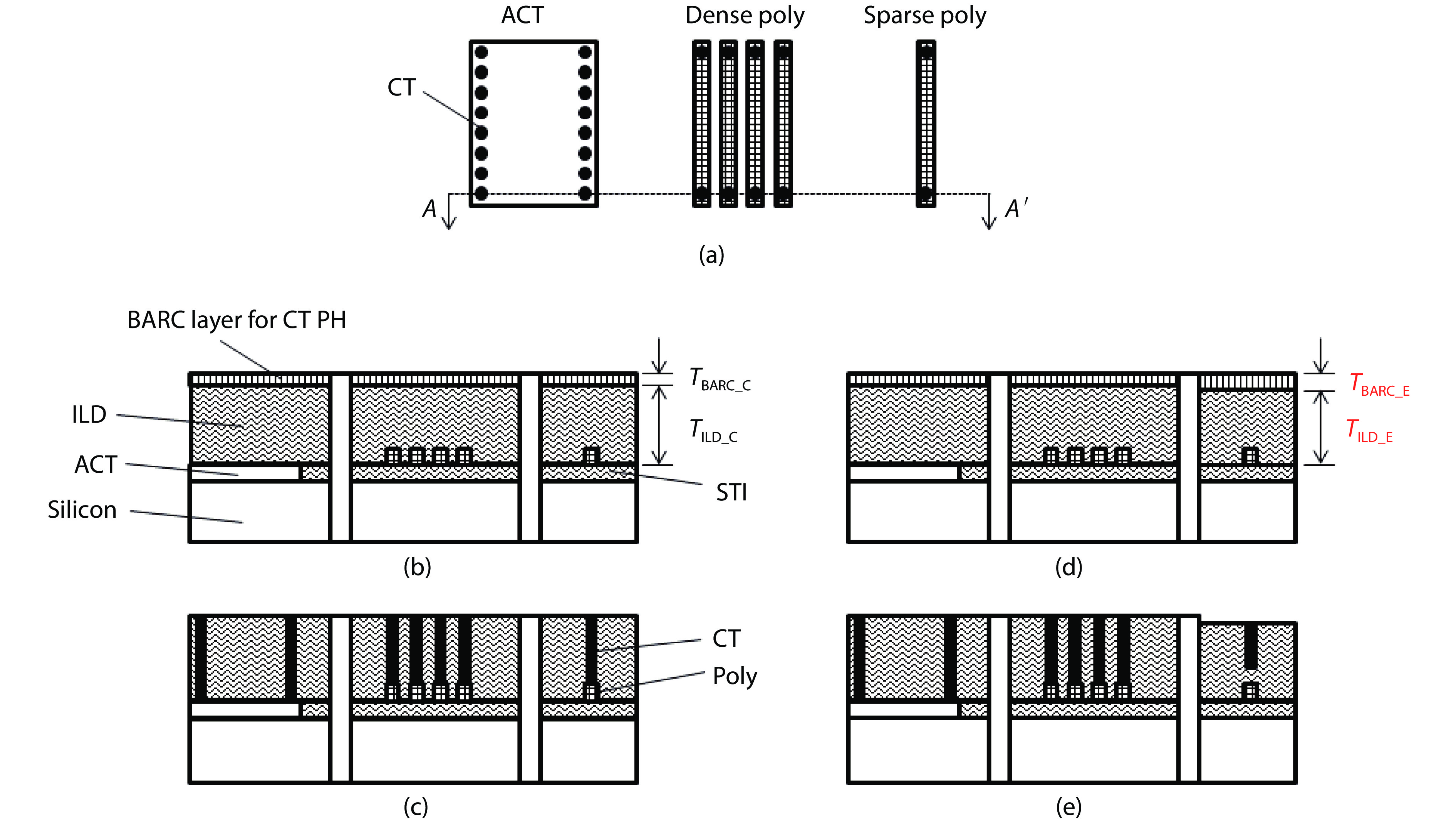
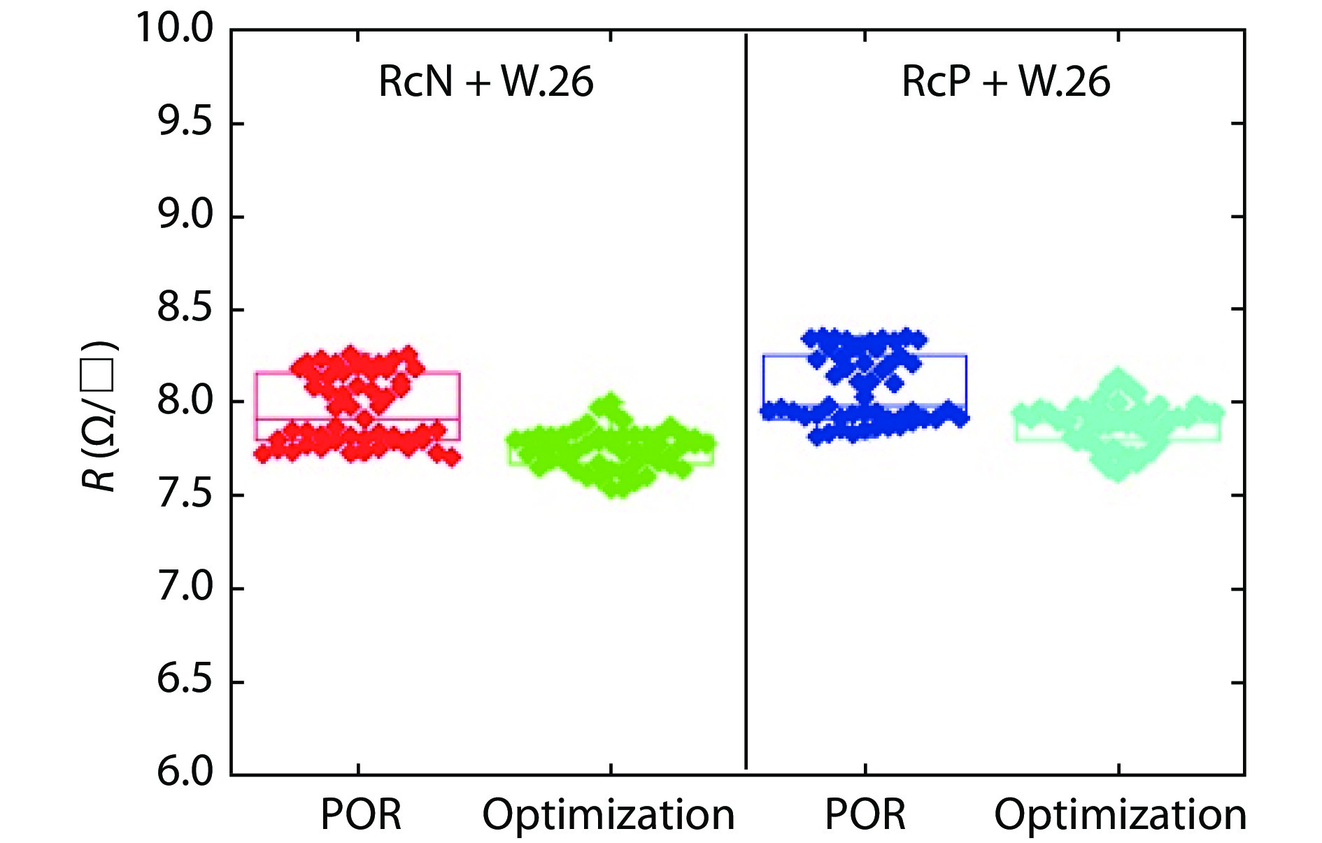
Radio-frequency (RF) process products suffer from a wafer edge low yield issue, which is induced by contact opening. A failure mechanism has been proposed that is based on the characteristics of a wafer edge film stack. The large step height at the wafer’s edge leads to worse planarization for the sparse poly-pattern region during the inter-layer dielectric (ILD) chemical mechanical polishing (CMP) process. A thicker bottom anti-reflect coating (BARC) layer was introduced for a sparse poly-pattern at the wafer edge region. The contact open issue was solved by increasing the break through (BT) time to get a large enough window. Well profile and resistance uniformity were obtained by contact etch recipe optimization.-
Keywords:
- bottom anti-reflect coating,
- break through,
- wafer edge,
- planarization
-
References
[1] Esfeh B K, Rack M, Ali K B, et al. RF small- and large-signal characteristics of CPW and TFMS lines on trap-rich HR-SOI substrates. IEEE Trans Electron Devices, 2018, 65, 3120 doi: 10.1109/TED.2018.2845679[2] Jaffe M, Abou-Khalil M, Botula A, et al. Improvements in SOI technology for RF switches. IEEE 15th Topical Meeting on Silicon Monolithic Integrated Circuits in RF Systems, 2015, 30[3] Gianesello F, Monroy A, Vialla V, et al. Highly linear and sub 120 fs Ron × Coff 130 nm RF SOI technology targeting 5G carrier aggregation RF switches and FEM SOC. IEEE 16th Topical Meeting on Silicon Monolithic Integrated Circuits in RF Systems (SiRF), 2016, 9[4] Maleville C, Celler G. SOI: Challenges and solutions to increasing yield in an ultrathin age. Yield Management Solutions, 2004, 6[5] Delahaye B, Baltzinger J L, Denis L, et al. Edge and extreme edge wafer manufacturing on 200 mm wafer: methodology, yield challenges, cost effective solutions, limitations. IEEE/SEMI Advanced Semiconductor Manufacturing Conference, 2009, 100[6] Goh I A N, Chua H S, Neo T L, et al. An integrated engineering approach to improve wafer edge yield. IEEE International Symposium on Semiconductor Manufacturing Conference Proceedings, 2001, 351[7] Harris K R, Ang B Y. Yield implications of wafer edge engineering. International Symposium on Microelectronics & Assembly, 2000, 70[8] Plummer J D, Deal M D, Griffin P B. Silicon VLSI technology. Beijing: Publishing House of Electronics Industry, 2003[9] Quirk M, Serda J. Semiconductor manufacturing technology. Beijing: Publishing House of Electronics Industry, 2006[10] Men Y W, Zhang H, Zhou K, et al. Wafer back pressure control and optimization in the CMP process. J Semicond, 2011, 32, 126002 doi: 10.1088/1674-4926/32/12/126002[11] Zhou J W, Liu Y L, Zhang W. Study of CMP lapping technique of ULSI silicon substrate. J Semicond, 2007, 28, 572[12] Boumerzoug M. Optimized BARC films and etch byproduct removal for wafer edge defectivity reduction. 25th Annual SEMI Advanced Semiconductor Manufacturing Conference, 2014, 330[13] Hu H S, Zhang M. Modeling for charging effect during RIE processing. Chin J Electron, 2000, 28, 81[14] Ding H T, Yang Z C, Yan G Z. A dual-purpose method to enhance heat transfer and prevent notching effect in deep reactive ion etching. Chin J Electron, 2010, 38, 1201 -
Proportional views


 DownLoad:


