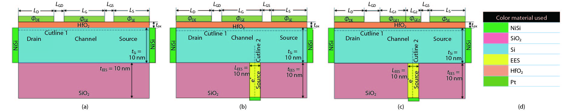
Fig. 1.
(Color online) Cross sectional view (a) CP-TFET, (b) DS-CP-TFET, (c) DS-DG-CP-TFET, and (d) color bar of materials.
ARTICLES
Shivendra Yadav1, , Alish Pamnani1, Dheeraj Sharma1, Anju Gedam2, Atul Kumar1 and Neeraj Sharma3
Corresponding author: Shivendra Yadav, shivendra1307@gmail.com
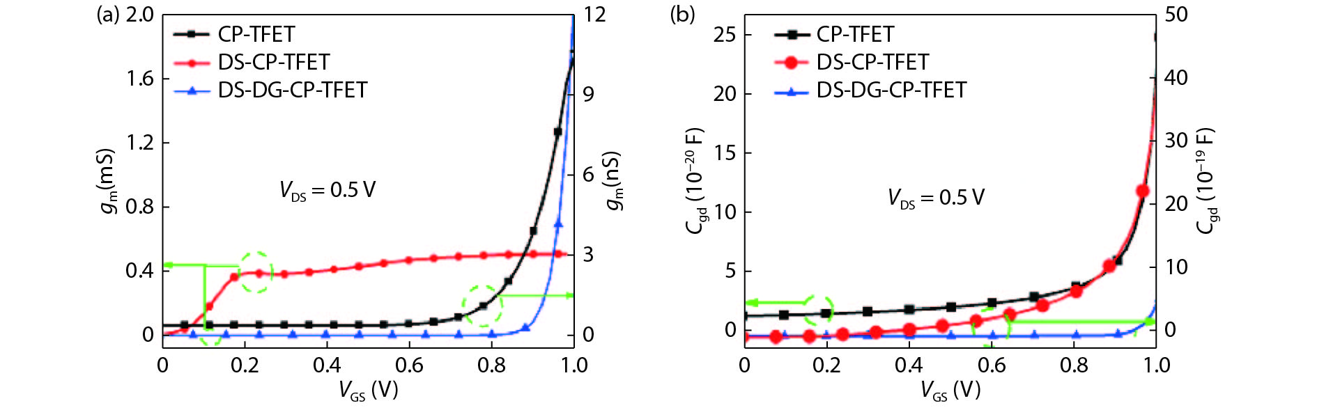
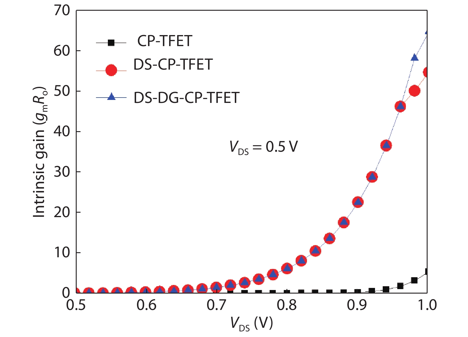
Abstract: In this paper, the impact of extra electron source (EES) and dual metal gate engineering on conventional charge plasma TFET (CP-TFET) have been done for improving DC and analog/RF parameters. CP-TFET structure is upgraded to double source CP-TFET (DS-CP-TFET) by placing an EES below the source/channel junction for enhancing the device performance in terms of driving current and RF figures of merit (FOMs). But, in spite of these pros, the approach is having cons of higher leakage current similar to MOSFET and negative conductance (inherent nature of TFET). Both the issues have been resolved in the double source dual gate CP-TFET (DS-DG-CP-TFET) by gate workfunction engineering and drain underlapping respectively. Additionally, for getting the optimum performance of DS-DG-CP-TFET, the device sensitivity has been investigated in terms of position of EES, length of drain electrode and workfunction of gate electrode 1 (GE1).
Keywords: ambipolar current, charge plasma, EES and dual metal gate engineering
| [1] |
Dennard R H, Gaensslen F H, Yu H N, et al. Design of ion-implanted MOSFET's with very small physical dimensions. IEEE J Solid-State Circuits, 1999, 87, 668 doi: 10.1109/JSSC.1974.1050511
|
| [2] |
Gopalakrishnan K, Woo R, Jungemann C, et al. Impact ionization MOS (I-MOS)-Part II: Experimental results. IEEE Trans Electron Devices, 2005, 52, 77 doi: 10.1109/TED.2004.841345
|
| [3] |
Hajare R, Lakshminarayana C, Raghunandan G H, et al. Performance enhancement of FINFET and CNTFET at different node technologies. Microsyst Technol, 2016, 22, 1121 doi: 10.1007/s00542-015-2468-9
|
| [4] |
International Technology Roadmap for Semiconductors (ITRS).[Online]. Available: www.itrs2.net
|
| [5] |
Koswatta S O, Lundstrom M S, Nikonov D E. Performance comparison between p-i-n tunneling transistors and conventional MOSFETs. IEEE Trans Electron Devices, 2009, 56, 456 doi: 10.1109/TED.2008.2011934
|
| [6] |
damrongplasit N, Kim S H, Liu T J K. Study of random dopant fluctuation induced variability in the raised-Ge source TFET. IEEE Electron Device Lett, 2013, 34, 184 doi: 10.1109/LED.2012.2235404
|
| [7] |
damrongplasit N, Shin C, Kim S H, et al. Study of random dopant fluctuation effects in germanium-source tunnel FETs. IEEE Trans Electron Devices, 2011, 58, 3541 doi: 10.1109/TED.2011.2161990
|
| [8] |
Jhaveri R, Nagavarapu V, Woo J C S. Effect of pocket doping and annealing schemes on the source-pocket tunnel field-effect transistor. IEEE Trans Electron Devices, 2011, 58, 80 doi: 10.1109/TED.2010.2089525
|
| [9] |
Kumar M J, Nadda K. Bipolar charge-plasma transistor:a novel three terminal device. IEEE Trans Electron Devices, 2012, 59, 962 doi: 10.1109/TED.2012.2184763
|
| [10] |
Kroemer H. Negative conductance in semiconductors. IEEE Spectrum, 1968, 5, 47 doi: 10.1109/MSPEC.1968.5215632
|
| [11] |
Yadav S, Sharma D, Chandan B V, et al. A novel hetero-material gate-underlap electrically doped TFET for improving DC/RF and ambipolar behaviour. Superlattices Microstruct, 2018, 117, 9 doi: 10.1016/j.spmi.2018.02.005
|
| [12] |
Polishchuk I, Ranade P, King T J, et al. Dual work function CMOS gate technology based on metal interdiffusion. U.S. Patent, no. US 2004O238859A1, 2004
|
| [13] |
Aaltonen T, Ritala M, Sajavaara T, et al. Atomic layer deposition of platinum thin films. Chem Mater, 2018, 15, 1924 doi: 10.1021/cm021333t
|
| [14] |
Gossenberger F, Roman T, Tonigold K F, et al. Change of the work function of platinum electrodes induced by halide adsorption. Beilst J Nanotechnol, 2014, 5, 152 doi: 10.3762/bjnano.5.15
|
| [15] |
Rajasekharan B, Hueting R J E, Salm C, et al. Fabrication and characterization of the charge-plasma diode. IEEE Electron Device Lett, 2010, 31, 528 doi: 10.1109/LED.2010.2045731
|
| [16] |
Kumar M J, Janardhanan S. Doping-less tunnel field effect transistor: Design and investigation. IEEE Trans Electron Devices, 2013, 60, 3285 doi: 10.1109/TED.2013.2276888
|
| [17] |
Lahgere A, Sahu C, Singh J. Electrically doped dynamically configurable field-effect transistor for low-power and high-performance applications. Electron Lett, 2015, 51, 1284 doi: 10.1049/el.2015.0079
|
| [18] |
Awadhiya B, Pandey S, Nigam K, et al. Effect of ITC's on linearity and distortion performance of junctionless tunnel field effect transistor. Superlattices Microstruct, 2017, 111, 293 doi: 10.1016/j.spmi.2017.06.036
|
| [19] |
ATLAS Device Simulation Software. Silvaco Int., Santa Clara, 2014
|
| [20] |
Boucart K, Ionescu A M. Double-gate tunnel FET with high-k gate dielectric. IEEE Trans Electron Devices, 2007, 54, 1725 doi: 10.1109/TED.2007.899389
|
| [21] |
Wang P F, Hilsenbeck K, Nirschl T, et al. Complementary tunneling transistor for low power application. Solid State Electron, 2004, 48, 2281 doi: 10.1016/j.sse.2004.04.006
|
| [22] |
Raad B R, Tirkey S, Sharma D, et al. A new design approach of dopingless tunnel FET for enhancement of device characteristics. IEEE Trans Electron Devices, 2017, 64, 1830 doi: 10.1109/TED.2017.2672640
|
| [23] |
Pahwa G, Dutta T, Agarwal A, et al. Analysis and compact modeling of negative capacitance transistor with high ON-current and negative output differential resistance Part II: model validation. IEEE Trans Electron Devices, 2017, 63, 4986 doi: 10.1109/ted.2016.2614436
|
| [24] |
Cho S, Lee J S, Kim K R, et al. Analyses on small-signal parameters and radio-frequency modeling of gate-all-around tunneling field-effect transistors. IEEE Trans Electron Devices, 2011, 58, 4164 doi: 10.1109/TED.2011.2167335
|
| [25] |
Yang Y, Tong X, Yang L T, et al. Tunneling field-effect transistor: Capacitance components and modeling. IEEE Electron Device Lett, 2010, 31, 752 doi: 10.1109/LED.2010.2047240
|
| [26] |
Goswami Y, Ghosh B, Asthana P K, et al. Analog performance of Si junctionless tunnel field effect transistor and its improvisation using II–IV semiconductor. R Soc Chem, 2014, 4, 10761 doi: 10.1039/c3ra46535g
|
| [27] |
Madan J, Chaujar R. Gate drain-overlapped-asymmetric gate dielectric-GAA-TFET: a solution for suppressed ambipolarity and enhanced ON state behavior. Appl Phys A, 2016, 122, 973 doi: 10.1007/s00339-016-0510-0
|
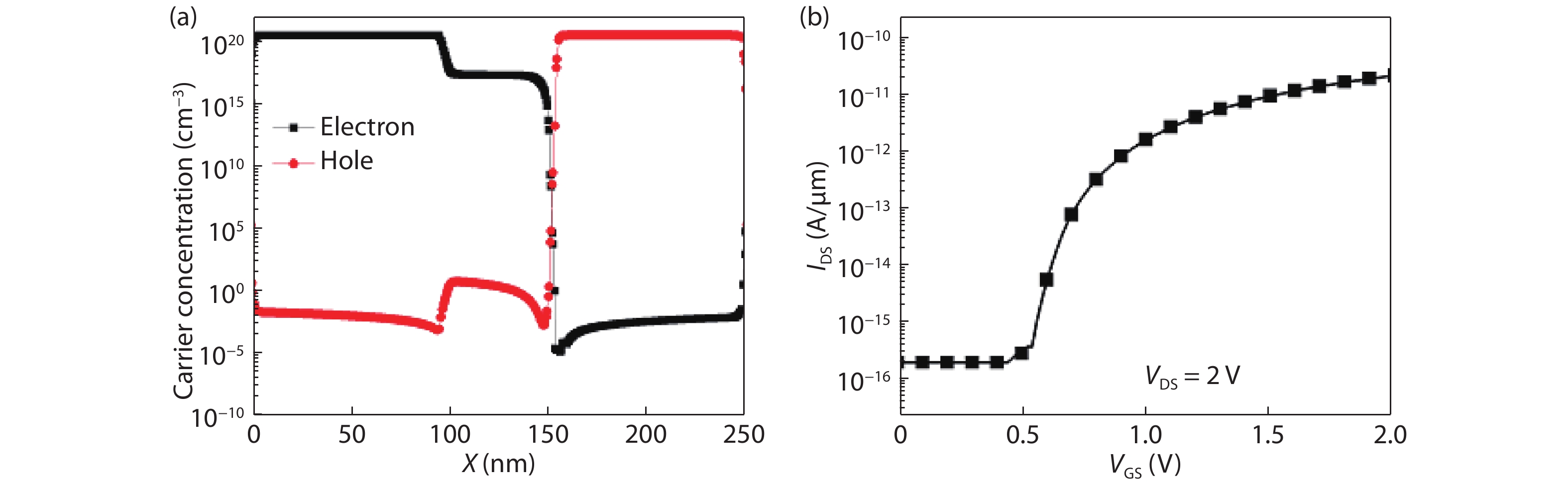
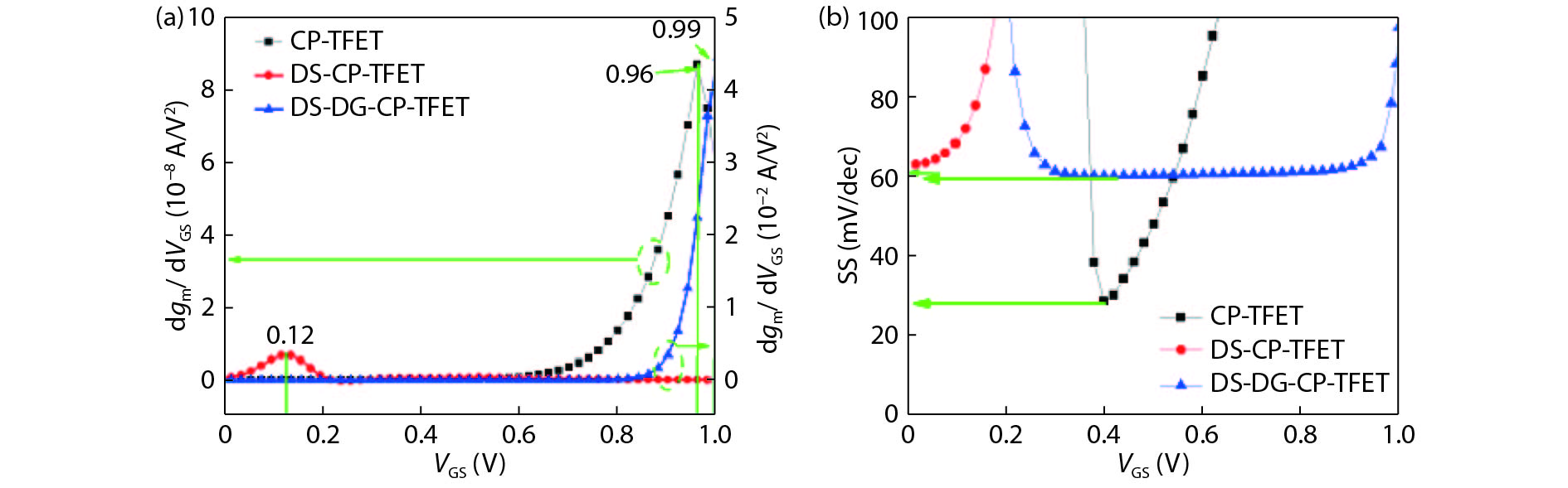
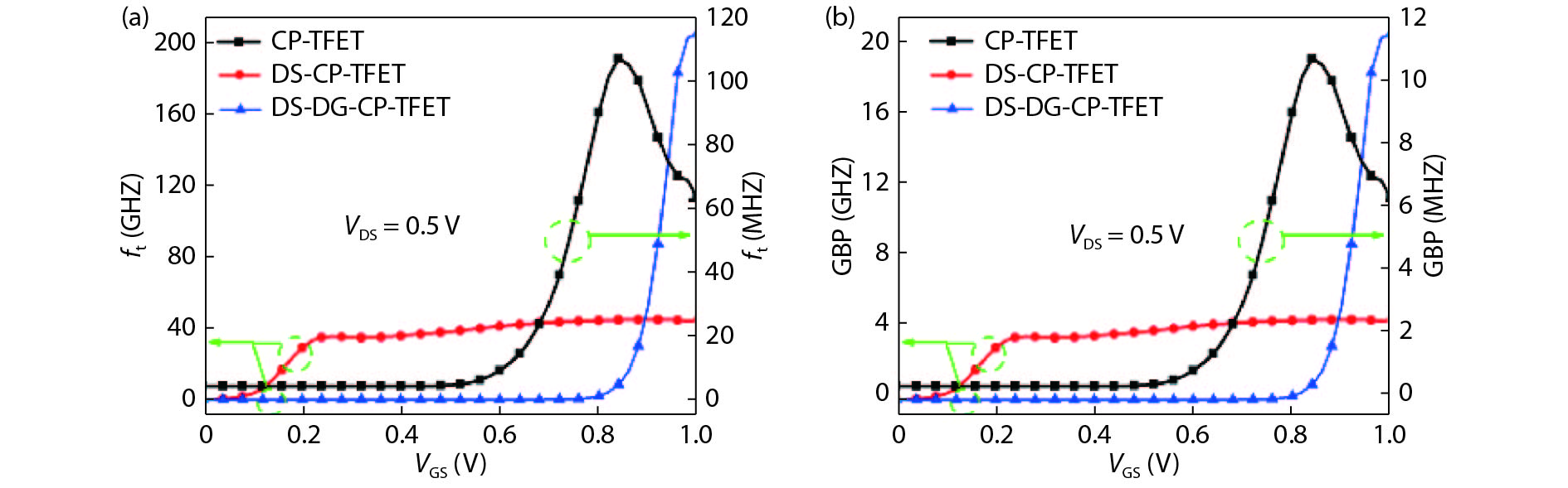
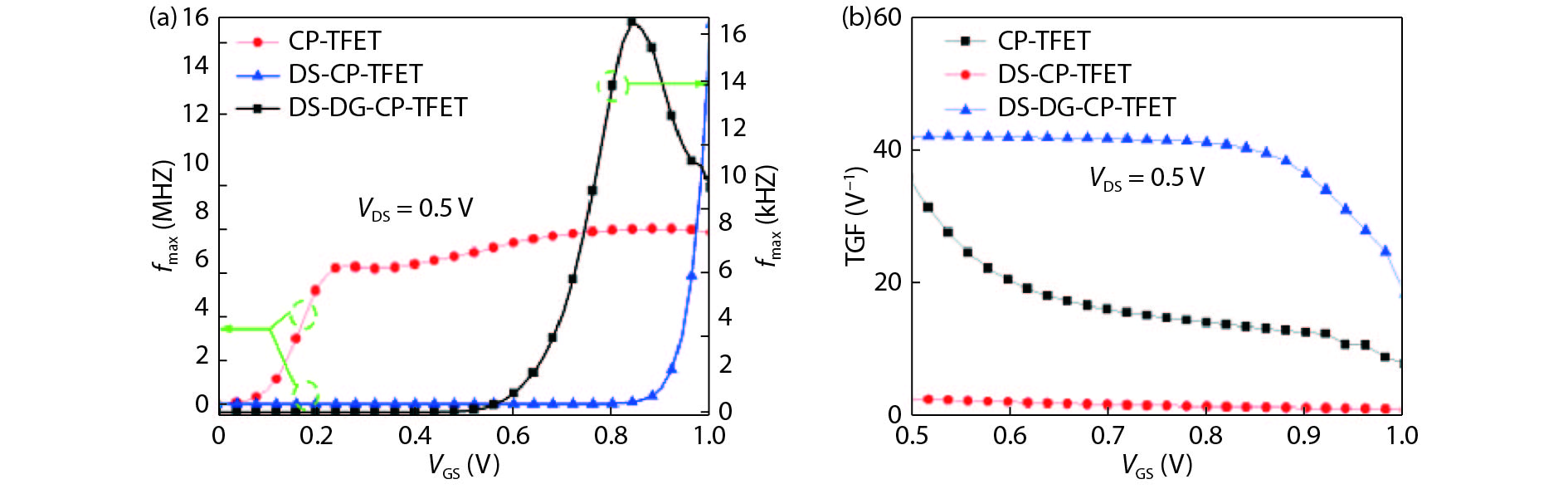
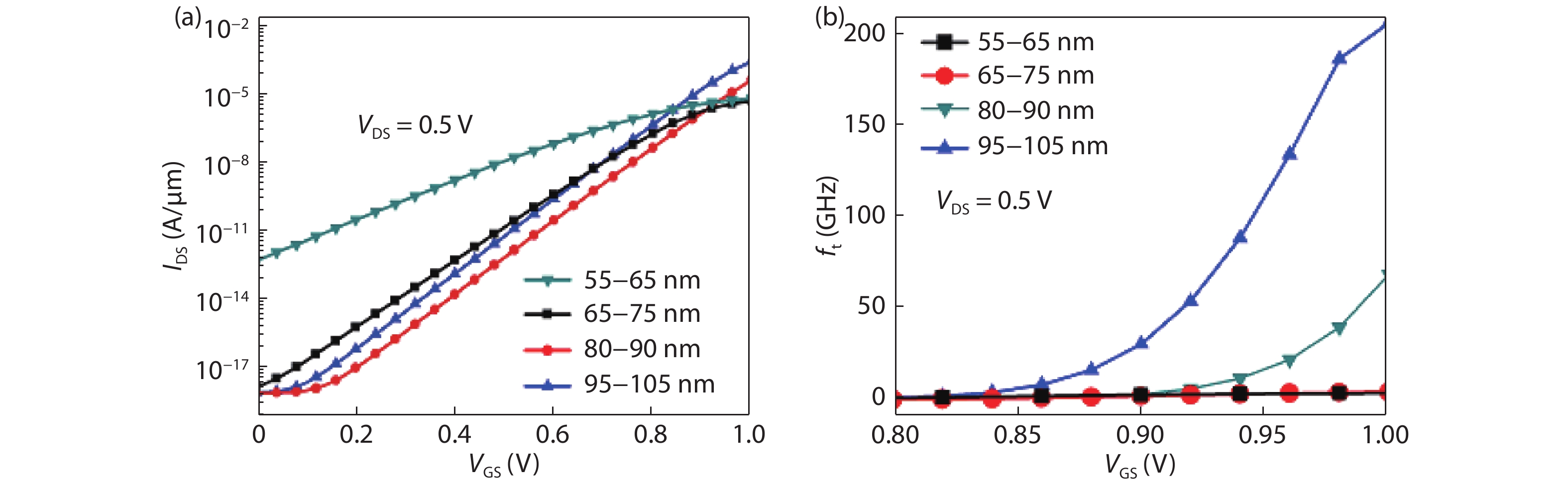
Table 1. DC parameters of devices.
| Parameters name/Unit | CP-TFET | DS-CP-TFET | DM-DG-CP-TFET |
  | 0.12 | 0.96 | 0.99 |
ON current (A/  | 1.067 × 10⁻⁹ | 3.794 × 10⁻⁵ | 3.238 × 10⁻⁴ |
OFF current (A/  | 5.078 × 10⁻¹⁸ | 6.013 × 10⁻⁹ | 5.219 × 10⁻¹⁸ |
Ambipolar current (A/  | 9.184 × 10⁻¹¹ | 1.983 × 10⁻¹¹ | 5.204 × 10⁻¹⁸ |
| SS (mV/dec) | 28.8 | 61.6 | 59.8 |
 DownLoad: CSV
| [1] |
Dennard R H, Gaensslen F H, Yu H N, et al. Design of ion-implanted MOSFET's with very small physical dimensions. IEEE J Solid-State Circuits, 1999, 87, 668 doi: 10.1109/JSSC.1974.1050511
|
| [2] |
Gopalakrishnan K, Woo R, Jungemann C, et al. Impact ionization MOS (I-MOS)-Part II: Experimental results. IEEE Trans Electron Devices, 2005, 52, 77 doi: 10.1109/TED.2004.841345
|
| [3] |
Hajare R, Lakshminarayana C, Raghunandan G H, et al. Performance enhancement of FINFET and CNTFET at different node technologies. Microsyst Technol, 2016, 22, 1121 doi: 10.1007/s00542-015-2468-9
|
| [4] |
International Technology Roadmap for Semiconductors (ITRS).[Online]. Available: www.itrs2.net
|
| [5] |
Koswatta S O, Lundstrom M S, Nikonov D E. Performance comparison between p-i-n tunneling transistors and conventional MOSFETs. IEEE Trans Electron Devices, 2009, 56, 456 doi: 10.1109/TED.2008.2011934
|
| [6] |
damrongplasit N, Kim S H, Liu T J K. Study of random dopant fluctuation induced variability in the raised-Ge source TFET. IEEE Electron Device Lett, 2013, 34, 184 doi: 10.1109/LED.2012.2235404
|
| [7] |
damrongplasit N, Shin C, Kim S H, et al. Study of random dopant fluctuation effects in germanium-source tunnel FETs. IEEE Trans Electron Devices, 2011, 58, 3541 doi: 10.1109/TED.2011.2161990
|
| [8] |
Jhaveri R, Nagavarapu V, Woo J C S. Effect of pocket doping and annealing schemes on the source-pocket tunnel field-effect transistor. IEEE Trans Electron Devices, 2011, 58, 80 doi: 10.1109/TED.2010.2089525
|
| [9] |
Kumar M J, Nadda K. Bipolar charge-plasma transistor:a novel three terminal device. IEEE Trans Electron Devices, 2012, 59, 962 doi: 10.1109/TED.2012.2184763
|
| [10] |
Kroemer H. Negative conductance in semiconductors. IEEE Spectrum, 1968, 5, 47 doi: 10.1109/MSPEC.1968.5215632
|
| [11] |
Yadav S, Sharma D, Chandan B V, et al. A novel hetero-material gate-underlap electrically doped TFET for improving DC/RF and ambipolar behaviour. Superlattices Microstruct, 2018, 117, 9 doi: 10.1016/j.spmi.2018.02.005
|
| [12] |
Polishchuk I, Ranade P, King T J, et al. Dual work function CMOS gate technology based on metal interdiffusion. U.S. Patent, no. US 2004O238859A1, 2004
|
| [13] |
Aaltonen T, Ritala M, Sajavaara T, et al. Atomic layer deposition of platinum thin films. Chem Mater, 2018, 15, 1924 doi: 10.1021/cm021333t
|
| [14] |
Gossenberger F, Roman T, Tonigold K F, et al. Change of the work function of platinum electrodes induced by halide adsorption. Beilst J Nanotechnol, 2014, 5, 152 doi: 10.3762/bjnano.5.15
|
| [15] |
Rajasekharan B, Hueting R J E, Salm C, et al. Fabrication and characterization of the charge-plasma diode. IEEE Electron Device Lett, 2010, 31, 528 doi: 10.1109/LED.2010.2045731
|
| [16] |
Kumar M J, Janardhanan S. Doping-less tunnel field effect transistor: Design and investigation. IEEE Trans Electron Devices, 2013, 60, 3285 doi: 10.1109/TED.2013.2276888
|
| [17] |
Lahgere A, Sahu C, Singh J. Electrically doped dynamically configurable field-effect transistor for low-power and high-performance applications. Electron Lett, 2015, 51, 1284 doi: 10.1049/el.2015.0079
|
| [18] |
Awadhiya B, Pandey S, Nigam K, et al. Effect of ITC's on linearity and distortion performance of junctionless tunnel field effect transistor. Superlattices Microstruct, 2017, 111, 293 doi: 10.1016/j.spmi.2017.06.036
|
| [19] |
ATLAS Device Simulation Software. Silvaco Int., Santa Clara, 2014
|
| [20] |
Boucart K, Ionescu A M. Double-gate tunnel FET with high-k gate dielectric. IEEE Trans Electron Devices, 2007, 54, 1725 doi: 10.1109/TED.2007.899389
|
| [21] |
Wang P F, Hilsenbeck K, Nirschl T, et al. Complementary tunneling transistor for low power application. Solid State Electron, 2004, 48, 2281 doi: 10.1016/j.sse.2004.04.006
|
| [22] |
Raad B R, Tirkey S, Sharma D, et al. A new design approach of dopingless tunnel FET for enhancement of device characteristics. IEEE Trans Electron Devices, 2017, 64, 1830 doi: 10.1109/TED.2017.2672640
|
| [23] |
Pahwa G, Dutta T, Agarwal A, et al. Analysis and compact modeling of negative capacitance transistor with high ON-current and negative output differential resistance Part II: model validation. IEEE Trans Electron Devices, 2017, 63, 4986 doi: 10.1109/ted.2016.2614436
|
| [24] |
Cho S, Lee J S, Kim K R, et al. Analyses on small-signal parameters and radio-frequency modeling of gate-all-around tunneling field-effect transistors. IEEE Trans Electron Devices, 2011, 58, 4164 doi: 10.1109/TED.2011.2167335
|
| [25] |
Yang Y, Tong X, Yang L T, et al. Tunneling field-effect transistor: Capacitance components and modeling. IEEE Electron Device Lett, 2010, 31, 752 doi: 10.1109/LED.2010.2047240
|
| [26] |
Goswami Y, Ghosh B, Asthana P K, et al. Analog performance of Si junctionless tunnel field effect transistor and its improvisation using II–IV semiconductor. R Soc Chem, 2014, 4, 10761 doi: 10.1039/c3ra46535g
|
| [27] |
Madan J, Chaujar R. Gate drain-overlapped-asymmetric gate dielectric-GAA-TFET: a solution for suppressed ambipolarity and enhanced ON state behavior. Appl Phys A, 2016, 122, 973 doi: 10.1007/s00339-016-0510-0
|


Article views: 4405 Times PDF downloads: 67 Times Cited by: 0 Times
Received: 08 February 2019 Revised: 18 March 2019 Online: Accepted Manuscript: 15 April 2019Uncorrected proof: 17 April 2019Published: 08 May 2019
| Citation: |
Shivendra Yadav, Alish Pamnani, Dheeraj Sharma, Anju Gedam, Atul Kumar, Neeraj Sharma. A novel design approach of charge plasma tunnel FET for radio frequency applications[J]. Journal of Semiconductors, 2019, 40(5): 052901. doi: 10.1088/1674-4926/40/5/052901
****
S Yadav, A Pamnani, D Sharma, A Gedam, A Kumar, N Sharma, A novel design approach of charge plasma tunnel FET for radio frequency applications[J]. J. Semicond., 2019, 40(5): 052901. doi: 10.1088/1674-4926/40/5/052901.

|
| [1] |
Dennard R H, Gaensslen F H, Yu H N, et al. Design of ion-implanted MOSFET's with very small physical dimensions. IEEE J Solid-State Circuits, 1999, 87, 668 doi: 10.1109/JSSC.1974.1050511
|
| [2] |
Gopalakrishnan K, Woo R, Jungemann C, et al. Impact ionization MOS (I-MOS)-Part II: Experimental results. IEEE Trans Electron Devices, 2005, 52, 77 doi: 10.1109/TED.2004.841345
|
| [3] |
Hajare R, Lakshminarayana C, Raghunandan G H, et al. Performance enhancement of FINFET and CNTFET at different node technologies. Microsyst Technol, 2016, 22, 1121 doi: 10.1007/s00542-015-2468-9
|
| [4] |
International Technology Roadmap for Semiconductors (ITRS).[Online]. Available: www.itrs2.net
|
| [5] |
Koswatta S O, Lundstrom M S, Nikonov D E. Performance comparison between p-i-n tunneling transistors and conventional MOSFETs. IEEE Trans Electron Devices, 2009, 56, 456 doi: 10.1109/TED.2008.2011934
|
| [6] |
damrongplasit N, Kim S H, Liu T J K. Study of random dopant fluctuation induced variability in the raised-Ge source TFET. IEEE Electron Device Lett, 2013, 34, 184 doi: 10.1109/LED.2012.2235404
|
| [7] |
damrongplasit N, Shin C, Kim S H, et al. Study of random dopant fluctuation effects in germanium-source tunnel FETs. IEEE Trans Electron Devices, 2011, 58, 3541 doi: 10.1109/TED.2011.2161990
|
| [8] |
Jhaveri R, Nagavarapu V, Woo J C S. Effect of pocket doping and annealing schemes on the source-pocket tunnel field-effect transistor. IEEE Trans Electron Devices, 2011, 58, 80 doi: 10.1109/TED.2010.2089525
|
| [9] |
Kumar M J, Nadda K. Bipolar charge-plasma transistor:a novel three terminal device. IEEE Trans Electron Devices, 2012, 59, 962 doi: 10.1109/TED.2012.2184763
|
| [10] |
Kroemer H. Negative conductance in semiconductors. IEEE Spectrum, 1968, 5, 47 doi: 10.1109/MSPEC.1968.5215632
|
| [11] |
Yadav S, Sharma D, Chandan B V, et al. A novel hetero-material gate-underlap electrically doped TFET for improving DC/RF and ambipolar behaviour. Superlattices Microstruct, 2018, 117, 9 doi: 10.1016/j.spmi.2018.02.005
|
| [12] |
Polishchuk I, Ranade P, King T J, et al. Dual work function CMOS gate technology based on metal interdiffusion. U.S. Patent, no. US 2004O238859A1, 2004
|
| [13] |
Aaltonen T, Ritala M, Sajavaara T, et al. Atomic layer deposition of platinum thin films. Chem Mater, 2018, 15, 1924 doi: 10.1021/cm021333t
|
| [14] |
Gossenberger F, Roman T, Tonigold K F, et al. Change of the work function of platinum electrodes induced by halide adsorption. Beilst J Nanotechnol, 2014, 5, 152 doi: 10.3762/bjnano.5.15
|
| [15] |
Rajasekharan B, Hueting R J E, Salm C, et al. Fabrication and characterization of the charge-plasma diode. IEEE Electron Device Lett, 2010, 31, 528 doi: 10.1109/LED.2010.2045731
|
| [16] |
Kumar M J, Janardhanan S. Doping-less tunnel field effect transistor: Design and investigation. IEEE Trans Electron Devices, 2013, 60, 3285 doi: 10.1109/TED.2013.2276888
|
| [17] |
Lahgere A, Sahu C, Singh J. Electrically doped dynamically configurable field-effect transistor for low-power and high-performance applications. Electron Lett, 2015, 51, 1284 doi: 10.1049/el.2015.0079
|
| [18] |
Awadhiya B, Pandey S, Nigam K, et al. Effect of ITC's on linearity and distortion performance of junctionless tunnel field effect transistor. Superlattices Microstruct, 2017, 111, 293 doi: 10.1016/j.spmi.2017.06.036
|
| [19] |
ATLAS Device Simulation Software. Silvaco Int., Santa Clara, 2014
|
| [20] |
Boucart K, Ionescu A M. Double-gate tunnel FET with high-k gate dielectric. IEEE Trans Electron Devices, 2007, 54, 1725 doi: 10.1109/TED.2007.899389
|
| [21] |
Wang P F, Hilsenbeck K, Nirschl T, et al. Complementary tunneling transistor for low power application. Solid State Electron, 2004, 48, 2281 doi: 10.1016/j.sse.2004.04.006
|
| [22] |
Raad B R, Tirkey S, Sharma D, et al. A new design approach of dopingless tunnel FET for enhancement of device characteristics. IEEE Trans Electron Devices, 2017, 64, 1830 doi: 10.1109/TED.2017.2672640
|
| [23] |
Pahwa G, Dutta T, Agarwal A, et al. Analysis and compact modeling of negative capacitance transistor with high ON-current and negative output differential resistance Part II: model validation. IEEE Trans Electron Devices, 2017, 63, 4986 doi: 10.1109/ted.2016.2614436
|
| [24] |
Cho S, Lee J S, Kim K R, et al. Analyses on small-signal parameters and radio-frequency modeling of gate-all-around tunneling field-effect transistors. IEEE Trans Electron Devices, 2011, 58, 4164 doi: 10.1109/TED.2011.2167335
|
| [25] |
Yang Y, Tong X, Yang L T, et al. Tunneling field-effect transistor: Capacitance components and modeling. IEEE Electron Device Lett, 2010, 31, 752 doi: 10.1109/LED.2010.2047240
|
| [26] |
Goswami Y, Ghosh B, Asthana P K, et al. Analog performance of Si junctionless tunnel field effect transistor and its improvisation using II–IV semiconductor. R Soc Chem, 2014, 4, 10761 doi: 10.1039/c3ra46535g
|
| [27] |
Madan J, Chaujar R. Gate drain-overlapped-asymmetric gate dielectric-GAA-TFET: a solution for suppressed ambipolarity and enhanced ON state behavior. Appl Phys A, 2016, 122, 973 doi: 10.1007/s00339-016-0510-0
|

 WeChat ID
Journal of Semiconductors © 2017 All Rights Reserved 京ICP备05085259号-2