


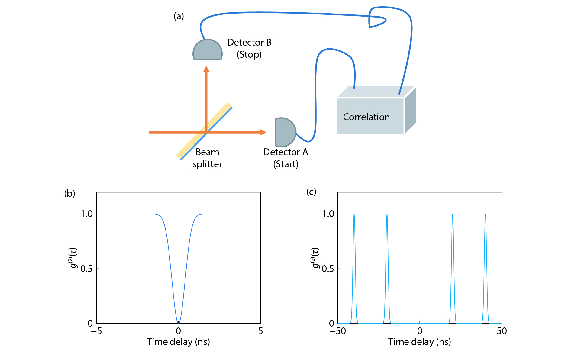
Fig. 1.
(Color online) (a) Schematic diagram of a Hanbury Brown and Twiss experiment. Second-order correlation function $ g^{(2)}$![]()
![]()
(τ) of an ideal SPS working in continuous wave mode (b) and pulse mode (c).
REVIEWS
Yating Lin, Yongzheng Ye and Wei Fang
Corresponding author: Wei Fang, Email: wfang08@zju.edu.cn
Abstract: Single-photon sources are building blocks for photonic quantum information processes. Of the many single-photon generation schemes, electrically driven single-photon sources have the advantages of realizing monolithic integration of quantum light sources and detectors without optical filtering, thus greatly simplify the integrated quantum photonic circuits. Here, we review recent advances on electrically driven single-photon sources based on solid-state quantum emitters, such as semiconductor epitaxial quantum dots, colloidal quantum dots, carbon nanotubes, molecules, and defect states in diamond, SiC and layered semiconductors. In particular, the merits and drawbacks of each system are discussed. Finally, the article is concluded by discussing the challenges that remain for electrically driven single-photon sources.
Keywords: single photon sources, electrically driven, integrated quantum photoncs
| [1] |
Nielsen M A, Chuang I L. Quantum computation and quantum information. Cambridge: Cambridge University Press, 2010
|
| [2] |
Sun Q C, Mao Y L, Chen S J, et al. Quantum teleportation with independent sources and prior entanglement distribution over a network. Nat Photon, 2016, 10(10), 671 doi: 10.1038/nphoton.2016.179
|
| [3] |
O’brien J L. Optical quantum computing. Science, 2007, 318(5856), 1567 doi: 10.1126/science.1142892
|
| [4] |
Arcari M, Söllner I, Javadi A, et al. Near-unity coupling efficiency of a quantum emitter to a photonic crystal waveguide. Phys Rev Lett, 2014, 113(9), 093603 doi: 10.1103/PhysRevLett.113.093603
|
| [5] |
Carolan J, Harrold C, Sparrow C, et al. Universal linear optics. Science, 2015, 349(6249), 711 doi: 10.1126/science.aab3642
|
| [6] |
Wang J, Paesani S, Ding Y, et al. Multidimensional quantum entanglement with large-scale integrated optics. Science, 2018, 360(6386), 285 doi: 10.1126/science.aar7053
|
| [7] |
Smith B J, Kundys D, Thomas-Peter N, et al. Phase-controlled integrated photonic quantum circuits. Opt Express, 2009, 17(16), 13516 doi: 10.1364/OE.17.013516
|
| [8] |
Takesue H, Matsuda N, Kuramochi E, et al. An on-chip coupled resonator optical waveguide single-photon buffer. Nat Commun, 2013, 4, 2725 doi: 10.1038/ncomms3725
|
| [9] |
Pernice W H, Schuck C, Minaeva O, et al. High-speed and high-efficiency travelling wave single-photon detectors embedded in nanophotonic circuits. Nat Commun, 2012, 3, 1325 doi: 10.1038/ncomms2307
|
| [10] |
Sprengers J, Gaggero A, Sahin D, et al. Waveguide superconducting single-photon detectors for integrated quantum photonic circuits. Appl Phys Lett, 2011, 99(18), 181110 doi: 10.1063/1.3657518
|
| [11] |
Senellart P, Solomon G, White A. High-performance semiconductor quantum-dot single-photon sources. Nat Nano, 2017, 12(11), 1026 doi: 10.1038/nnano.2017.218
|
| [12] |
Yuan Z, Kardynal B E, Stevenson R M, et al. Electrically driven single-photon source. Science, 2002, 295(5552), 102 doi: 10.1126/science.1066790
|
| [13] |
Ward M, Farrow T, See P, et al. Electrically driven telecommunication wavelength single-photon source. Appl Phys Lett, 2007, 90(6), 063512 doi: 10.1063/1.2472172
|
| [14] |
Deshpande S, Heo J, Das A, et al. Electrically driven polarized single-photon emission from an InGaN quantum dot in a GaN nanowire. Nat Commun, 2013, 4, 1675 doi: 10.1038/ncomms2691
|
| [15] |
Deshpande S, Frost T, Hazari A, et al. Electrically pumped single-photon emission at room temperature from a single In- GaN/GaN quantum dot. Appl Phys Lett, 2014, 105(14), 141109 doi: 10.1063/1.4897640
|
| [16] |
Nowak A, Portalupi S, Giesz V, et al. Deterministic and electrically tunable bright single-photon source. Nat Commun, 2014, 5, 3240 doi: 10.1038/ncomms4240
|
| [17] |
Heindel T, Schneider C, Lermer M, et al. Electrically driven quantum dot-micropillar single photon source with 34% overall efficiency. Appl Phys Lett, 2010, 96(1), 011107 doi: 10.1063/1.3284514
|
| [18] |
Lin X, Dai X, Pu C, et al. Electrically-driven single-photon sources based on colloidal quantum dots with near-optimal antibunching at room temperature. Nat Commun, 2017, 8(1), 1132 doi: 10.1038/s41467-017-01379-6
|
| [19] |
Khasminskaya S, Pyatkov F, Słowik K, et al. Fully integrated quantum photonic circuit with an electrically driven light source. Nat Photon, 2016, 10(11), 727 doi: 10.1038/nphoton.2016.178
|
| [20] |
Zhang L, Yu Y J, Chen L G, et al. Electrically driven single-photon emission from an isolated single molecule. Nat Commun, 2017, 8(1), 580 doi: 10.1038/s41467-017-00681-7
|
| [21] |
Lohrmann A, Pezzagna S, Dobrinets I, et al. Diamond based light-emitting diode for visible single-photon emission at room temperature. Appl Phys Lett, 2011, 99(25), 251106 doi: 10.1063/1.3670332
|
| [22] |
Mizuochi N, Makino T, Kato H, et al. Electrically driven single-photon source at room temperature in diamond. Nat Photon, 2012, 6(5), 299 doi: 10.1038/nphoton.2012.75
|
| [23] |
Doi Y, Makino T, Kato H, et al. Deterministic electrical charge-state initialization of single nitrogen-vacancy center in diamond. Phys Rev X, 2014, 4(1), 011057 doi: 10.1103/PhysRevX.4.011057
|
| [24] |
Lohrmann A, Iwamoto N, Bodrog Z, et al. Single-photon emitting diode in silicon carbide. Nat Commun, 2015, 6, 7783 doi: 10.1038/ncomms8783
|
| [25] |
Glauber R J. The quantum theory of optical coherence. Phys Rev, 1963, 130(6), 2529 doi: 10.1103/PhysRev.130.2529
|
| [26] |
Brown R H, Twiss R Q, surName g. Interferometry of the intensity fluctuations in light-i. basic theory: the correlation between photons in coherent beams of radiation. Proceedings of the Royal Society of London Series A Mathematical and Physical Sciences, 1957, 242(1230), 300 doi: 10.1098/rspa.1957.0177
|
| [27] |
Wang H, Duan Z C, Li Y H, et al. Near-transform-limited single photons from an efficient solid-state quantum emitter. Phys Rev Lett, 2016, 116(21), 213601 doi: 10.1103/PhysRevLett.116.213601
|
| [28] |
Hong C K, Ou Z Y, Mandel L. Measurement of subpicosecond time intervals between two photons by interference. Phys Rev Lett, 1987, 59(18), 2044 doi: 10.1103/PhysRevLett.59.2044
|
| [29] |
Imamog A, Yamamoto Y, et al. Turnstile device for heralded single photons: Coulomb blockade of electron and hole tunnel- ing in quantum confined p–i–n heterojunctions. Phys Rev Lett, 1994, 72(2), 210 doi: 10.1103/PhysRevLett.72.210
|
| [30] |
Gschrey M, Gericke F, Schüßler A, et al. In situ electron-beam lithography of deterministic single-quantum-dot mesa-structures using low-temperature cathodoluminescence spectroscopy. Appl Phys Lett, 2013, 102(25), 251113 doi: 10.1063/1.4812343
|
| [31] |
Somaschi N, Giesz V, De Santis L, et al. Near-optimal single-photon sources in the solid state. Nat Photonics, 2016, 10(5), 340 doi: 10.1038/nphoton.2016.23
|
| [32] |
Reischle M, Beirne G, Schulz W M, et al. Electrically pumped single-photon emission in the visible spectral range up to 80 K. Opt Express, 2008, 16(17), 12771 doi: 10.1364/OE.16.012771
|
| [33] |
Schlehahn A, Thoma A, Munnelly P, et al. An electrically driven cavity-enhanced source of indistinguishable photons with 61% overall efficiency. APL Photon, 2016, 1(1), 011301 doi: 10.1063/1.4939831
|
| [34] |
Deshpande S, Bhattacharya P. An electrically driven quantum dot-in-nanowire visible single photon source operating up to 150 K. Appl Phys Lett, 2013, 103(24), 241117 doi: 10.1063/1.4848195
|
| [35] |
Quitsch W, Kümmell T, Gust A, et al. Electrically driven single photon emission from a CdSe/ZnSSe single quantum dot at 200 K. Appl Phys Lett, 2014, 105(9), 091102 doi: 10.1063/1.4894729
|
| [36] |
Michler P, Imamoglu A, Mason M, et al. Quantum correlation among photons from a single quantum dot at room temperature. Nature, 2000, 406(6799), 968 doi: 10.1038/35023100
|
| [37] |
Högele A, Galland C, Winger M, et al. Photon antibunching in the photoluminescence spectra of a single carbon nanotube. Phys Rev Lett, 2008, 100(21), 217401 doi: 10.1103/PhysRevLett.100.217401
|
| [38] |
Sild O, Haller K. Zero-phonon lines: and spectral hole burning in spectroscopy and photochemistry. Berlin: Springer Science & Business Media, 2012
|
| [39] |
Lounis B, Moerner W E. Single photons on demand from a single molecule at room temperature. Nature, 2000, 407(6803), 491 doi: 10.1038/35035032
|
| [40] |
Nothaft M, Höhla S, Jelezko F, et al. Electrically driven photon antibunching from a single molecule at room temperature. Nat Commun, 2012, 3, 628 doi: 10.1038/ncomms1637
|
| [41] |
Doherty M W, Manson N B, Delaney P, et al. The nitrogen-vacancy colour centre in diamond. Phys Rep, 2013, 528(1), 1 doi: 10.1016/j.physrep.2013.02.001
|
| [42] |
Khramtsov I A, Agio M, Fedyanin D Y. Dynamics of single-photon emission from electrically pumped color centers. Phys Rev Appl, 2017, 8(2), 024031 doi: 10.1103/PhysRevApplied.8.024031
|
| [43] |
Özgür Ü, Alivov Y I, Liu C, et al. A comprehensive review of ZnO materials and devices. J Appl Phys, 2005, 98(4), 041301 doi: 10.1063/1.1992666
|
| [44] |
Choi S, Berhane A M, Gentle A, et al. Electroluminescence from localized defects in zinc oxide: toward electrically driven single photon sources at room temperature. ACS Appl Mater Interfaces, 2015, 7(10), 5619 doi: 10.1021/acsami.5b00340
|
| [45] |
Khramtsov I A, Vyshnevyy A A, Fedyanin D Y. Enhancing the brightness of electrically driven single-photon sources using color centers in silicon carbide. npj Quantum Inform, 2018, 4(1), 15 doi: 10.1038/s41534-018-0066-2
|
| [46] |
Manzeli S, Ovchinnikov D, Pasquier D, et al. 2D transition metal dichalcogenides. Nat Rev Mater, 2017, 2(8), 17033 doi: 10.1038/natrevmats.2017.33
|
| [47] |
Koperski M, Nogajewski K, Arora A, et al. Single photon emitters in exfoliated WSe2 structures. Nat Nano, 2015, 10(6), 503 doi: 10.1038/nnano.2015.67
|
| [48] |
Chakraborty C, Kinnischtzke L, Goodfellow K M, et al. Voltage-controlled quantum light from an atomically thin semicon- ductor. Nat Nano, 2015, 10(6), 507 doi: 10.1038/nnano.2015.79
|
| [49] |
He Y M, Clark G, Schaibley J R, et al. Single quantum emitters in monolayer semiconductors. Nat Nano, 2015, 10(6), 497 doi: 10.1038/nnano.2015.75
|
| [50] |
Palacios-berraquero C, Barbone M, Kara D M, et al. Atomically thin quantum light-emitting diodes. Nat Commun, 2016, 7, 12978 doi: 10.1038/ncomms12978
|
| [51] |
Tran T T, Bray K, Ford M J, et al. Quantum emission from hexagonal boron nitride monolayers. Nat Nano, 2016, 11(1), 37 doi: 10.1038/nnano.2015.242
|
| [52] |
Conterio M, Sköld N, Ellis D, et al. A quantum dot single photon source driven by resonant electrical injection. Appl Phys Lett, 2013, 103(16), 162108 doi: 10.1063/1.4825208
|


Article views: 5887 Times PDF downloads: 191 Times Cited by: 0 Times
Received: 01 July 2018 Revised: Online: Accepted Manuscript: 25 June 2019Uncorrected proof: 26 June 2019Published: 05 July 2019
| Citation: |
Yating Lin, Yongzheng Ye, Wei Fang. Electrically driven single-photon sources[J]. Journal of Semiconductors, 2019, 40(7): 071904. doi: 10.1088/1674-4926/40/7/071904
****
Y T Lin, Y Z Ye, W Fang, Electrically driven single-photon sources[J]. J. Semicond., 2019, 40(7): 071904. doi: 10.1088/1674-4926/40/7/071904.

|
| [1] |
Nielsen M A, Chuang I L. Quantum computation and quantum information. Cambridge: Cambridge University Press, 2010
|
| [2] |
Sun Q C, Mao Y L, Chen S J, et al. Quantum teleportation with independent sources and prior entanglement distribution over a network. Nat Photon, 2016, 10(10), 671 doi: 10.1038/nphoton.2016.179
|
| [3] |
O’brien J L. Optical quantum computing. Science, 2007, 318(5856), 1567 doi: 10.1126/science.1142892
|
| [4] |
Arcari M, Söllner I, Javadi A, et al. Near-unity coupling efficiency of a quantum emitter to a photonic crystal waveguide. Phys Rev Lett, 2014, 113(9), 093603 doi: 10.1103/PhysRevLett.113.093603
|
| [5] |
Carolan J, Harrold C, Sparrow C, et al. Universal linear optics. Science, 2015, 349(6249), 711 doi: 10.1126/science.aab3642
|
| [6] |
Wang J, Paesani S, Ding Y, et al. Multidimensional quantum entanglement with large-scale integrated optics. Science, 2018, 360(6386), 285 doi: 10.1126/science.aar7053
|
| [7] |
Smith B J, Kundys D, Thomas-Peter N, et al. Phase-controlled integrated photonic quantum circuits. Opt Express, 2009, 17(16), 13516 doi: 10.1364/OE.17.013516
|
| [8] |
Takesue H, Matsuda N, Kuramochi E, et al. An on-chip coupled resonator optical waveguide single-photon buffer. Nat Commun, 2013, 4, 2725 doi: 10.1038/ncomms3725
|
| [9] |
Pernice W H, Schuck C, Minaeva O, et al. High-speed and high-efficiency travelling wave single-photon detectors embedded in nanophotonic circuits. Nat Commun, 2012, 3, 1325 doi: 10.1038/ncomms2307
|
| [10] |
Sprengers J, Gaggero A, Sahin D, et al. Waveguide superconducting single-photon detectors for integrated quantum photonic circuits. Appl Phys Lett, 2011, 99(18), 181110 doi: 10.1063/1.3657518
|
| [11] |
Senellart P, Solomon G, White A. High-performance semiconductor quantum-dot single-photon sources. Nat Nano, 2017, 12(11), 1026 doi: 10.1038/nnano.2017.218
|
| [12] |
Yuan Z, Kardynal B E, Stevenson R M, et al. Electrically driven single-photon source. Science, 2002, 295(5552), 102 doi: 10.1126/science.1066790
|
| [13] |
Ward M, Farrow T, See P, et al. Electrically driven telecommunication wavelength single-photon source. Appl Phys Lett, 2007, 90(6), 063512 doi: 10.1063/1.2472172
|
| [14] |
Deshpande S, Heo J, Das A, et al. Electrically driven polarized single-photon emission from an InGaN quantum dot in a GaN nanowire. Nat Commun, 2013, 4, 1675 doi: 10.1038/ncomms2691
|
| [15] |
Deshpande S, Frost T, Hazari A, et al. Electrically pumped single-photon emission at room temperature from a single In- GaN/GaN quantum dot. Appl Phys Lett, 2014, 105(14), 141109 doi: 10.1063/1.4897640
|
| [16] |
Nowak A, Portalupi S, Giesz V, et al. Deterministic and electrically tunable bright single-photon source. Nat Commun, 2014, 5, 3240 doi: 10.1038/ncomms4240
|
| [17] |
Heindel T, Schneider C, Lermer M, et al. Electrically driven quantum dot-micropillar single photon source with 34% overall efficiency. Appl Phys Lett, 2010, 96(1), 011107 doi: 10.1063/1.3284514
|
| [18] |
Lin X, Dai X, Pu C, et al. Electrically-driven single-photon sources based on colloidal quantum dots with near-optimal antibunching at room temperature. Nat Commun, 2017, 8(1), 1132 doi: 10.1038/s41467-017-01379-6
|
| [19] |
Khasminskaya S, Pyatkov F, Słowik K, et al. Fully integrated quantum photonic circuit with an electrically driven light source. Nat Photon, 2016, 10(11), 727 doi: 10.1038/nphoton.2016.178
|
| [20] |
Zhang L, Yu Y J, Chen L G, et al. Electrically driven single-photon emission from an isolated single molecule. Nat Commun, 2017, 8(1), 580 doi: 10.1038/s41467-017-00681-7
|
| [21] |
Lohrmann A, Pezzagna S, Dobrinets I, et al. Diamond based light-emitting diode for visible single-photon emission at room temperature. Appl Phys Lett, 2011, 99(25), 251106 doi: 10.1063/1.3670332
|
| [22] |
Mizuochi N, Makino T, Kato H, et al. Electrically driven single-photon source at room temperature in diamond. Nat Photon, 2012, 6(5), 299 doi: 10.1038/nphoton.2012.75
|
| [23] |
Doi Y, Makino T, Kato H, et al. Deterministic electrical charge-state initialization of single nitrogen-vacancy center in diamond. Phys Rev X, 2014, 4(1), 011057 doi: 10.1103/PhysRevX.4.011057
|
| [24] |
Lohrmann A, Iwamoto N, Bodrog Z, et al. Single-photon emitting diode in silicon carbide. Nat Commun, 2015, 6, 7783 doi: 10.1038/ncomms8783
|
| [25] |
Glauber R J. The quantum theory of optical coherence. Phys Rev, 1963, 130(6), 2529 doi: 10.1103/PhysRev.130.2529
|
| [26] |
Brown R H, Twiss R Q, surName g. Interferometry of the intensity fluctuations in light-i. basic theory: the correlation between photons in coherent beams of radiation. Proceedings of the Royal Society of London Series A Mathematical and Physical Sciences, 1957, 242(1230), 300 doi: 10.1098/rspa.1957.0177
|
| [27] |
Wang H, Duan Z C, Li Y H, et al. Near-transform-limited single photons from an efficient solid-state quantum emitter. Phys Rev Lett, 2016, 116(21), 213601 doi: 10.1103/PhysRevLett.116.213601
|
| [28] |
Hong C K, Ou Z Y, Mandel L. Measurement of subpicosecond time intervals between two photons by interference. Phys Rev Lett, 1987, 59(18), 2044 doi: 10.1103/PhysRevLett.59.2044
|
| [29] |
Imamog A, Yamamoto Y, et al. Turnstile device for heralded single photons: Coulomb blockade of electron and hole tunnel- ing in quantum confined p–i–n heterojunctions. Phys Rev Lett, 1994, 72(2), 210 doi: 10.1103/PhysRevLett.72.210
|
| [30] |
Gschrey M, Gericke F, Schüßler A, et al. In situ electron-beam lithography of deterministic single-quantum-dot mesa-structures using low-temperature cathodoluminescence spectroscopy. Appl Phys Lett, 2013, 102(25), 251113 doi: 10.1063/1.4812343
|
| [31] |
Somaschi N, Giesz V, De Santis L, et al. Near-optimal single-photon sources in the solid state. Nat Photonics, 2016, 10(5), 340 doi: 10.1038/nphoton.2016.23
|
| [32] |
Reischle M, Beirne G, Schulz W M, et al. Electrically pumped single-photon emission in the visible spectral range up to 80 K. Opt Express, 2008, 16(17), 12771 doi: 10.1364/OE.16.012771
|
| [33] |
Schlehahn A, Thoma A, Munnelly P, et al. An electrically driven cavity-enhanced source of indistinguishable photons with 61% overall efficiency. APL Photon, 2016, 1(1), 011301 doi: 10.1063/1.4939831
|
| [34] |
Deshpande S, Bhattacharya P. An electrically driven quantum dot-in-nanowire visible single photon source operating up to 150 K. Appl Phys Lett, 2013, 103(24), 241117 doi: 10.1063/1.4848195
|
| [35] |
Quitsch W, Kümmell T, Gust A, et al. Electrically driven single photon emission from a CdSe/ZnSSe single quantum dot at 200 K. Appl Phys Lett, 2014, 105(9), 091102 doi: 10.1063/1.4894729
|
| [36] |
Michler P, Imamoglu A, Mason M, et al. Quantum correlation among photons from a single quantum dot at room temperature. Nature, 2000, 406(6799), 968 doi: 10.1038/35023100
|
| [37] |
Högele A, Galland C, Winger M, et al. Photon antibunching in the photoluminescence spectra of a single carbon nanotube. Phys Rev Lett, 2008, 100(21), 217401 doi: 10.1103/PhysRevLett.100.217401
|
| [38] |
Sild O, Haller K. Zero-phonon lines: and spectral hole burning in spectroscopy and photochemistry. Berlin: Springer Science & Business Media, 2012
|
| [39] |
Lounis B, Moerner W E. Single photons on demand from a single molecule at room temperature. Nature, 2000, 407(6803), 491 doi: 10.1038/35035032
|
| [40] |
Nothaft M, Höhla S, Jelezko F, et al. Electrically driven photon antibunching from a single molecule at room temperature. Nat Commun, 2012, 3, 628 doi: 10.1038/ncomms1637
|
| [41] |
Doherty M W, Manson N B, Delaney P, et al. The nitrogen-vacancy colour centre in diamond. Phys Rep, 2013, 528(1), 1 doi: 10.1016/j.physrep.2013.02.001
|
| [42] |
Khramtsov I A, Agio M, Fedyanin D Y. Dynamics of single-photon emission from electrically pumped color centers. Phys Rev Appl, 2017, 8(2), 024031 doi: 10.1103/PhysRevApplied.8.024031
|
| [43] |
Özgür Ü, Alivov Y I, Liu C, et al. A comprehensive review of ZnO materials and devices. J Appl Phys, 2005, 98(4), 041301 doi: 10.1063/1.1992666
|
| [44] |
Choi S, Berhane A M, Gentle A, et al. Electroluminescence from localized defects in zinc oxide: toward electrically driven single photon sources at room temperature. ACS Appl Mater Interfaces, 2015, 7(10), 5619 doi: 10.1021/acsami.5b00340
|
| [45] |
Khramtsov I A, Vyshnevyy A A, Fedyanin D Y. Enhancing the brightness of electrically driven single-photon sources using color centers in silicon carbide. npj Quantum Inform, 2018, 4(1), 15 doi: 10.1038/s41534-018-0066-2
|
| [46] |
Manzeli S, Ovchinnikov D, Pasquier D, et al. 2D transition metal dichalcogenides. Nat Rev Mater, 2017, 2(8), 17033 doi: 10.1038/natrevmats.2017.33
|
| [47] |
Koperski M, Nogajewski K, Arora A, et al. Single photon emitters in exfoliated WSe2 structures. Nat Nano, 2015, 10(6), 503 doi: 10.1038/nnano.2015.67
|
| [48] |
Chakraborty C, Kinnischtzke L, Goodfellow K M, et al. Voltage-controlled quantum light from an atomically thin semicon- ductor. Nat Nano, 2015, 10(6), 507 doi: 10.1038/nnano.2015.79
|
| [49] |
He Y M, Clark G, Schaibley J R, et al. Single quantum emitters in monolayer semiconductors. Nat Nano, 2015, 10(6), 497 doi: 10.1038/nnano.2015.75
|
| [50] |
Palacios-berraquero C, Barbone M, Kara D M, et al. Atomically thin quantum light-emitting diodes. Nat Commun, 2016, 7, 12978 doi: 10.1038/ncomms12978
|
| [51] |
Tran T T, Bray K, Ford M J, et al. Quantum emission from hexagonal boron nitride monolayers. Nat Nano, 2016, 11(1), 37 doi: 10.1038/nnano.2015.242
|
| [52] |
Conterio M, Sköld N, Ellis D, et al. A quantum dot single photon source driven by resonant electrical injection. Appl Phys Lett, 2013, 103(16), 162108 doi: 10.1063/1.4825208
|

 WeChat ID
Journal of Semiconductors © 2017 All Rights Reserved 京ICP备05085259号-2

 DownLoad:

