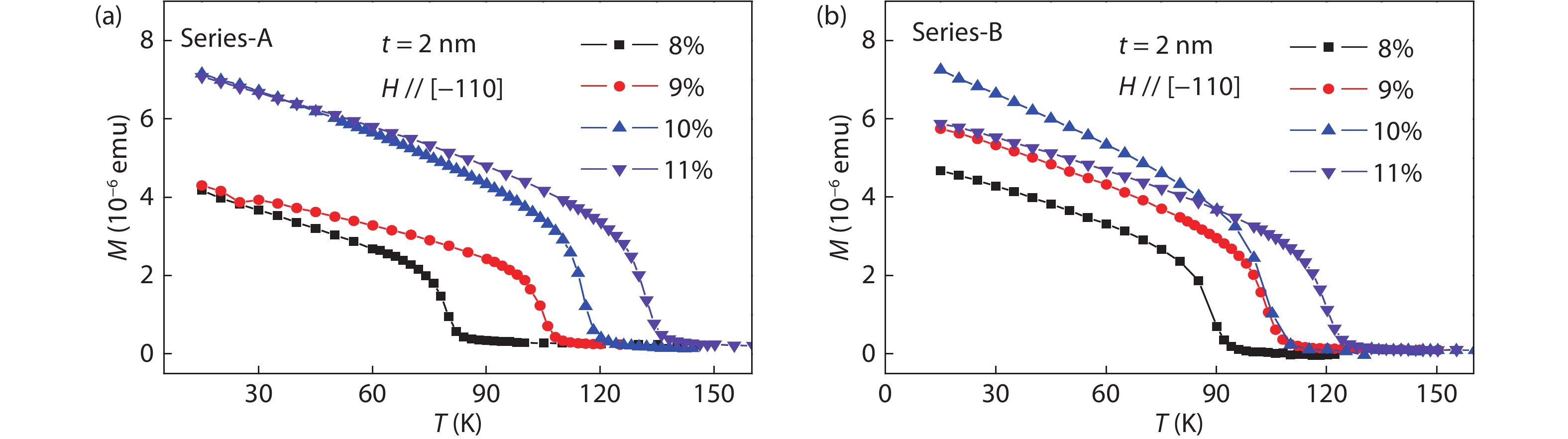
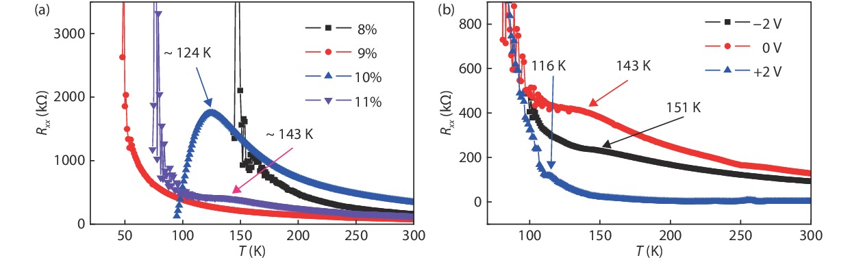
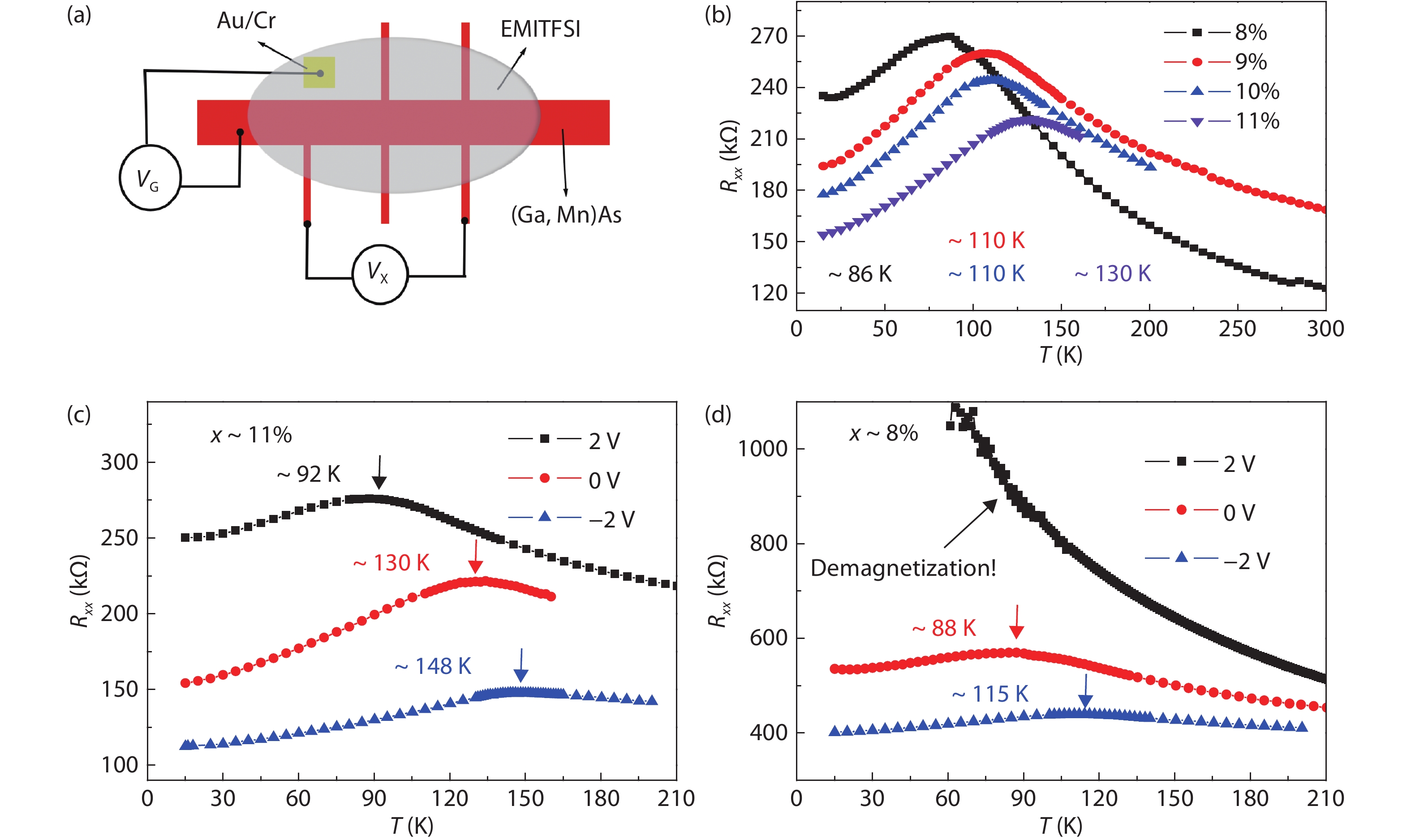
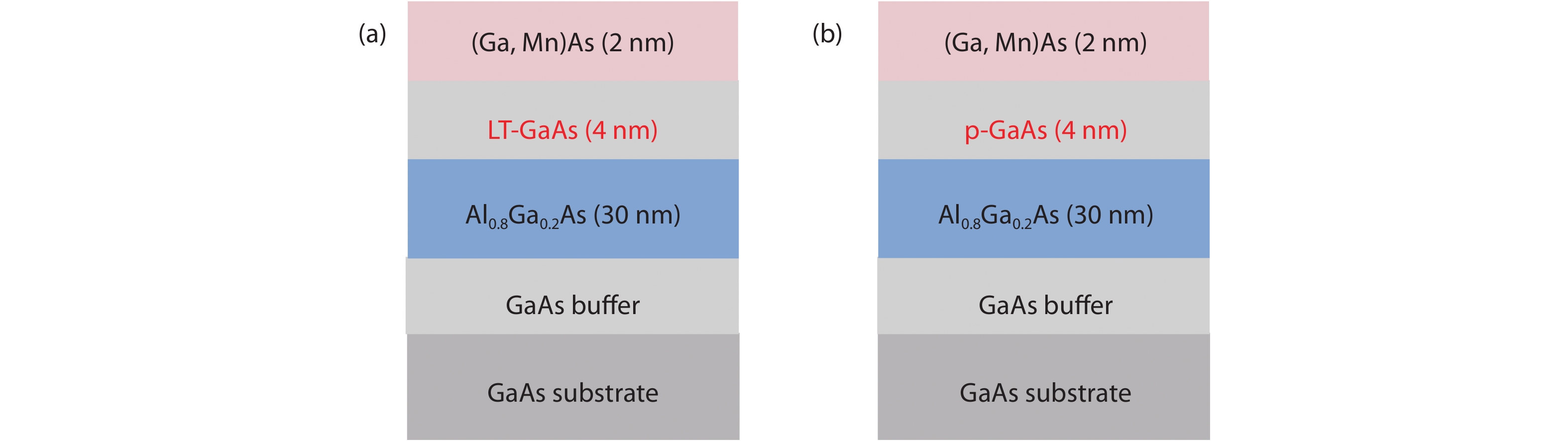
J. Semicond. > 2019, Volume 40 > Issue 9 > 092501

ARTICLES

Giant modulation of magnetism in (Ga,Mn)As ultrathin films via electric field

Hailong Wang1, 2, Jialin Ma1, 2 and Jianhua Zhao1, 2, 3,

+ Author Affiliations

 Corresponding author: Jianhua Zhao, jhzhao@red.semi.ac.cn

DOI: 10.1088/1674-4926/40/9/092501

PDF

Turn off MathJax

Abstract: Taking the advantages of semiconducting properties and carrier-mediated ferromagnetism in (Ga,Mn)As, a giant modulation of magnetism via electric field in (Ga,Mn)As ultrathin film has been demonstrated. Specifically, huge interfacial electric field is obtained by using ionic liquid as the gate dielectric. Both magnetization and transport measurements are employed to characterize the samples, while the transport data are used to analyze the electric filed effect on magnetism. Complete demagnetization of (Ga,Mn)As film is then realized by thinning its thickness down to ~2 nm, during which the degradation of ferromagnetism of (Ga,Mn)As ultrathin film induced by quantum confinement effect is suppressed by inserting a heavily-doped p-type GaAs buffer layer. The variation of the Curie temperature is more than 100 K, which is nearly 5-times larger than previous results. Our results provide a new pathway on the efficient electrical control of magnetism.

Key words: (Ga,Mn)As filmelectric-field effectCurie temperaturedemagnetization

Attributed to its scaling down capability and potential advantage on significantly lowering the power consumption, electrical control of magnetism has been one of the hottest topics in the research of spintronics[1]. For instances, magnetization reversal by spin transfer and/or spin-orbit torque, and magnetic domain wall motion by spin-polarized current have been extensively studied and proved to be very promising[15]. The ultimate goal of the endeavor is definitely to decrease the switching energy of a single magnetic bit to its theoretical limit, in which controlling the magnetism in nanoscale through applying an electric field is one of the most attractive methods.

As one of the very first demonstrations, dilute magnetic semiconductors (DMS) have played a very critical role, due to their features of combining carrier-mediated ferromagnetism and relatively low carrier density together[611]. Among these materials, (Ga,Mn)As has been investigated most extensively, based on which electric-field control of Curie temperature (TC), saturation magnetization (Ms), coercive field (Hc), magnetic anisotropy and magnetization vector rotation has all been successfully realized[1215]. So far, previous reports were mainly focusing on the mechanism of the electrical control of magnetism, and/or exploited this method to investigate the rich physics in (Ga,Mn)As and related heterostructures[615]. As a fundamental question, it is also interesting to know to what extent one can manipulate the magnetism in (Ga,Mn)As films experimentally[16].

In principle, the main obstacles that restrict the electric-field effect on the magnetism in (Ga,Mn)As lie in two aspects: firstly, stronger ferromagnetism requires larger hole density, which will then decrease the penetration depth of the electric-field and limit the electric-field effect; secondly, thinning down the (Ga,Mn)As films to less than ~5 nm usually makes it insulating and even destroys its ferromagnetism. Correspondingly, two routes could be employed to partly figure out these problems: one is using advanced techniques that can apply larger electric-field than the upper limit of conventional gating method, which usually uses solid state dielectrics as the gate insulator and results in a highest breakdown strength of electric-field of ~ 1 V/nm[1721]; the second way is trying to maintain the ferromagnetism of (Ga,Mn)As while decreasing its thickness[14, 15, 22]. For the first solution, ionic liquid and organic molecules have shown their power by presenting enhanced manipulation capability[1721]. However, experiments adopting the second method are still rare[1721].

In this work, by a special layer structure design which suppresses the hole depletion near the interface of (Ga,Mn)As and GaAs or (Al,Ga)As layers, we successfully grew ferromagnetic ultrathin (Ga,Mn)As films with thickness down to ~2 nm. Moreover, these samples maintain relatively high TC (~100 K) and metallic transport properties. Furthermore, by using ionic liquid as the gate dielectric, giant modulation of magnetism via electric-field in (Ga,Mn)As thin film was realized. As indicated by the transport measurements, the largest variation of TC exceeds 100 K, which is nearly 5-times larger than previous results. Our results provide a new pathway for the efficient electrical control of magnetism in (Ga,Mn)As.

Two series of (Ga,Mn)As samples with thickness of ~2 nm were grown on GaAs (001) substrates by molecular-beam epitaxy (MBE), which are named as series-A and series-B samples, respectively. All the underlayers were deposited at ~560 °C, while the (Ga,Mn)As layer was grown at ~220 °C. In each set of samples, four (Ga,Mn)As samples with nominal Mn concentration of ~8%, 9%, 10% and 11% are prepared. The main difference between these two sets of samples is that the low-temperature grown GaAs or (Al,Ga)As underlayer in conventional layer structure were replaced by a heavily Be-doped GaAs layer. The layer structure is shown in Fig. 1, and the sample information is listed in Table 1. The doping concentration of the Be-doped GaAs is about 2 × 1019 cm–3, while its thickness is 4 nm, the same with the low-temperature GaAs layer. It is well known that the hole density in (Ga,Mn)As with TC higher than 100 K is usually in the range of 5 × 10¹⁹–2 × 1021 cm–3, which will be partly depleted at the interface, especially when the underlayer is low temperature grown n-type GaAs layer. This depletion phenomenon is not important when (Ga,Mn)As film is thick enough, but can be very crucial for ultrathin films, which might account for the insulating tendency of ultrathin (Ga,Mn)As films. Moreover, the hole-mediated ferromagnetism of (Ga,Mn)As will also be strongly weakened as a result of the hole depletion. For the above reasons, the heavily p-doped GaAs layers in series-B samples are expected to suppress the depletion of holes and the tendency of being insulating (or even loss of ferromagnetism) in (Ga,Mn)As ultrathin films.

Figure  1.  (Color online) Schematic diagrams of the layer structure for (a) series-A and (b) series-B samples. The (Al,Ga)As buffer layer plays the role of an energy barrier, and the low-temperature grown n-type GaAs in series-A samples will deplete the holes in (Ga,Mn)As film to some extent, while the heavily-doped p-type GaAs layers in series-B samples are used to suppress the hole depletion.
Table  1.  Detailed information of series-A and series-B samples.
Parameter Series-A Series-B
A1 A2 A3 A4 B1 B2 B3 B4
Mn (%) 8 9 10 11 8 9 10 11
Thickness (nm) ~2 ~2 ~2 ~2 ~2 ~2 ~2 ~2
Underlayer LT-GaAs (n-type) Be-doped GaAs (p-type)
DownLoad: CSV  | Show Table

After being taken out from the MBE chamber, the (Ga,Mn)As samples were then annealed in the atmosphere at 220 °C for 1 h. Subsequently, 3-nm-thick HfO2 was deposited at 100 °C on (Ga,Mn)As by atomic layer deposition (ALD), during which the pulses of Hf(NMe2)4 and de-ionized water were alternatively generated with N2 purging between each period. The HfO2 can protect the ultrathin (Ga,Mn)As film from being damaged by the following device fabrication processes. The samples were then patterned into Hall-bar devices (10–30 μm wide) using photo-lithography and argon ion beam etching, following which an isolated Au/Cr electrode was formed by thermal evaporation and lift-off processes. Ionic liquid 1-ethyl-3-methyl imidazolium bis(trifluoromethylsulfonyl)imide (EMITFSI) was then dropped on the Hall device as the gate dielectric.

Figs. 2(a) and 2(b) show the temperature dependent magnetization curves for these two series of heavily Mn-doped (Ga,Mn)As samples. A magnetic field of 20 Oe was applied along the GaAs [–110] direction, in order to cover the unknown influence of the residual magnetic field from the superconducting magnet in our magnetometer. As can be seen, all the samples exhibit well-defined ferromagnetism with their Curie temperatures ranging from around 80 to 135 K. It is clear that TC of both sets of samples increases with the increase of Mn content. However, no consistent enhancement of TC is observed for series-B samples, although they are expected to show stronger ferromagnetism due to the less depletion of holes near the interface. Notice that TC of sample B4 with 11% Mn content is higher than sample B3, but its magnetization at low temperature is smaller. The lower TC of sample B3 might be attributed to the strong compensation of holes by As antisites, while the lower magnetization for sample B4 can be ascribed to the antiferromagnetic Mn–Mn exchange interation (direct exchange without the assistance of holes).

Figure  2.  (Color online) Temperature dependence of the magnetization for (a) series-A and (b) series-B samples. The magnetic field of 20 Oe is applied along the (Ga,Mn)As [–110] direction. An enhancement of TC with the increase of Mn content can be clearly observed, while there is no obvious difference between the magnetic properties of these two series of samples.

As for the transport properties, we mainly focus on the temperature dependence of longitudinal resistance (R–T curves). Figs. 3(a) and 4(b) plots the R–T curves for both series of samples, and the results are very different. For series-A samples, the sample resistances increase rapidly when decreasing the temperature and even become unmeasurable except sample A3 with 10% Mn content. On the contrast, the sample resistances of series-B samples increase first and then decrease with decreasing the temperature, similar with the typical behaviors of metallic thick (Ga,Mn)As films. In comparison with the transport results of series-A samples, we conclude that the heavily-doped p-GaAs underlayer does suppress the depletion of holes in (Ga,Mn)As to some extent, although it does not show observable influence on their magnetization data.

Figure  3.  (Color online) (a) Longitudinal resistance as a function of temperature for series-A samples. (b) Temperature dependent longitudinal resistances of sample A4 under gate voltages, in which the peak shifts to lower (higher) temperature when the applied voltage is +2 V (–2 V).
Figure  4.  (Color online) (a) Schematic of the device structure. (b) Longitudinal resistance as a function of temperature for series-B samples. (c, d) Temperature dependent longitudinal resistances for samples B4 and B1 under various gate voltages, in which clear peak shifts can be observed.

It is well established that the R–T curves of metallic (Ga,Mn)As sample can be used to estimate its TC, which is roughly corresponding to the metal-insulator transition temperature[2326]. It is worth mentioning that accurate determination of TC by R–T curves is difficult, since the correspondence between TC and the peak of R–T or dR/dT–T curves was not always correct. Experimentally, they are found to be sample dependent, although some people claim that the peak of dR/dT–T curves should be used to determine TC in optimized and uniform (Ga,Mn)As samples[27, 28]. For simplicity, here we use the peak of R–T curves to characterize TC. It is clear that the peak of each R–T curve indeed appears near TC.

The gate electric-field was applied between the isolated electrode and one of the current leads, as shown in Fig. 4(a). The R–T curve was then recorded with the gate voltage (VG) fixed at a certain value during the whole measurement process. Fig. 3(b) presents the results for sample A4 with 11% nominal Mn content, and clear change of the resistance can be observed when the gate voltage is changed from –2 to 2 V. Fortunately, all three curves show a transition peak despite the resistance becomes too large to show a good signal to noise ratio (SNR). Specifically, the peak of its RT curve shifts to lower (higher) temperature when the applying VG is +2 V (–2 V), which can be ascribed to the depletion (accumulation) of holes in the ultrathin (Ga,Mn)As channel, and is consistent with previous theoretical and experimental results[1022]. As discussed above, the modulation range of TC can then be roughly determined to be from ~116 to 151 K, with a large variation magnitude of ~35 K. This value is comparable with that achieved by using organic molecules and several times larger than the typical value obtained by using conventional solid-state gating method.

Fig. 4(c) shows the gating results for sample B4, which has the same nominal Mn content with sample A4. Similar shifts of the peak occurred, and in the whole temperature range good SNR ratios were obtained. Under the same gate voltage range, TC changes from ~92 to ~148 K, resulting in a variation magnitude of ~56 K. This is a further improvement of the gating capability, much larger than the values achieved in previous reports[1022]. Notice that the magnetism of sample B4 is relatively hard to tune due to its higher Mn and hole density, as indicated by the resistance shown in Fig. 4(b). Therefore, extended electric-field effect on magnetism is expected for the samples with lower Mn and hole concentration. In Fig. 4(d), the gating results for sample B1 is presented, in which an increase of TC from ~87 to ~115 K is observed. Moreover, the peak of the R–T curve disappears when applying +2 V to the sample, and the resistance rapidly increases to be larger than 1 MΩ. In consideration of the hole-mediated ferromagnetism in (Ga,Mn)As, this insulting behavior probably indicates that sample B1 is demagnetized in the whole temperature, which means a variation of TC of ~115 K via electric-field. We note here that more experimental evidences, especially the challenging magnetization data with applying gate voltage that can be directly measured by magnetometers are needed to confirm this inference.

Finally, we want to discuss the details of the differences between the two series of samples qualitatively. At first, it should be pointed out that the annealing effect would probably be different, because the diffusion energy potential for the interstitial Mn2+ (Mnint) is not the same: for series-A samples, a large built-in electric-field in the (Ga,Mn)As/n-GaAs p–n junction would prevent the diffusion of the Mnint ions, while this effect is much weaker in (Ga,Mn)As/p-GaAs junction. Combining with the magnetic measurement results, it can be infer that the hole density in series-A samples is larger than that of series-B samples. However, according to the transport measurements, the effective thicknesses within which the hole density is large enough to maintain the ferromagnetism of the series-A samples should in general be smaller than the series-B samples (probably except sample A3). These two factors, i.e., the effective thickness and the hole density, interplay with each other, and result in the coexistence of similar magnetic behaviors and quite different transport properties.

In conclusion, by replacing the n-GaAs or (Al,Ga)As underlayers in conventional sample structures with p+-GaAs, we successfully grew ferromagnetic metallic ultrathin (Ga,Mn)As films with thickness down to ~2 nm. Furthermore, large interfacial electric-field near the (Ga,Mn)As layer was realized by using ionic liquid as the gate dielectric, which results in a giant modulation of magnetism in these ultrathin (Ga,Mn)As films. As indicated by the transport measurement, the largest variation of TC exceeds 100 K, in which a demagnetization in a wide temperature range was observed. Our results are nearly five times larger than previous results obtained by gating, and are also much larger than that achieved by using organic molecules. Our results prove the feasibility of enhancing the electric-field effect on magnetism by thinning down the (Ga,Mn)As samples, which provide a new pathway for the efficient electrical control of magnetism in (Ga,Mn)As.

This work is supported by MOST (Grant No. 2017YFB0405701), and NSFC (Grants Nos. U1632264 and 11704374), and the Key Research Project of Frontier Science of Chinese Academy of Science (Grant No. QYZDY-SSW-JSC015).


[1]
Matsukura F, Tokura Y, Ohno H. Control of magnetism by electric fields. Nat Nanotech, 2015, 10(3), 209 doi: 10.1038/nnano.2015.22
[2]
Ralph D C, Stiles M D. Spin transfer torques. J Magn Magn Mater, 2008, 320(7), 1190 doi: 10.1016/j.jmmm.2007.12.019
[3]
Yamanouchi M, Chiba D, Matsukura F, et al. Current-induced domain-wall switching in a ferromagnetic semiconductor structure. Nature, 2004, 428(6982), 539 doi: 10.1038/nature02441
[4]
Chernyshov A, Overby M, Liu X Y, et al. Evidence for reversible control of magnetization in a ferromagnetic material by means of spin-orbit magnetic field. Nat Phys, 2009, 5(9), 656 doi: 10.1038/nphys1362
[5]
Miron I M, Gaudin G, Auffret S, et al. Current-driven spin torque induced by the Rashba effect in a ferromagnetic metal layer. Nat Mater, 2010, 9(3), 230 doi: 10.1038/nmat2613
[6]
Ohno H. Making nonmagnetic semiconductors ferromagnetic. Science, 1998, 281(5379), 951 doi: 10.1126/science.281.5379.951
[7]
Dietl T, Ohno H, Matsukura F, et al. Zener model description of ferromagnetism in zinc-blende magnetic semiconductors. Science, 2000, 287(5455), 1019 doi: 10.1126/science.287.5455.1019
[8]
Jungwirth T, Sinova J, Masek J, et al. Theory of ferromagnetic (III,Mn)V semiconductors. Rev Mod Phys, 2006, 78(3), 809 doi: 10.1103/RevModPhys.78.809
[9]
Sato K, Bergqvist L, Kudrnovsky J, et al. First-principles theory of dilute magnetic semiconductors. Rev Mod Phys, 2010, 82(2), 1633 doi: 10.1103/RevModPhys.82.1633
[10]
Dietl T, Ohno H. Dilute ferromagnetic semiconductors: Physics and spintronic structures. Rev Mod Phys, 2014, 86(1), 187 doi: 10.1103/RevModPhys.86.187
[11]
Jungwirth T, Wunderlich J, Novak V, et al. Spin-dependent phenomena and device concepts explored in (Ga,Mn)As. Rev Mod Phys, 2014, 86(3), 855 doi: 10.1103/RevModPhys.86.855
[12]
Chiba D, Matsukura F, Ohno H. Electric-field control of ferromagnetism in (Ga,Mn)As. Appl Phys Lett, 2006, 89, 162505 doi: 10.1063/1.2362971
[13]
Chiba D, Sawicki M, Nishitani Y, et al. Magnetization vector manipulation by electric fields. Nature, 2008, 455(7212), 515 doi: 10.1038/nature07318
[14]
Sawicki M, Chiba D, Korbecka A, et al. Experimental probing of the interplay between ferromagnetism and localization in (Ga,Mn)As. Nat Phys, 2010, 6(1), 22 doi: 10.1038/nphys1455
[15]
Chiba D, Werpachowska A, Endo M, et al. Anomalous Hall effect in field-effect structures of (Ga,Mn)As. Phys Rev Lett, 2010, 104, 106601 doi: 10.1103/PhysRevLett.104.106601
[16]
Wang H L, Wang X L, Xiong P, et al. Control of magnetism in dilute magnetic semiconductor (Ga,Mn)As films by surface decoration of molecules. Front Phys, 2016, 4, 9 doi: 10.3389/fphy.2016.00009
[17]
Endo M, Chiba D, Shimotani H, et al. Electric double layer transistor with a (Ga,Mn)As channel. Appl Phys Lett, 2010, 96, 022515 doi: 10.1063/1.3277146
[18]
Wang H L, Ma J L, Yu X Z, et al. Electric-field assisted switching of magnetization in perpendicularly magnetized (Ga,Mn)As films at high temperatures. J Phys D, 2017, 50, 025003 doi: 10.1088/1361-6463/50/2/025003
[19]
Ohno H. A window on the future of spintronics. Nat Mater, 2010, 9(12), 952 doi: 10.1038/nmat2913
[20]
Wang X L, Wang H L, Pan D, et al. Robust manipulation of magnetism in dilute magnetic semiconductor (Ga,Mn)As by organic molecules. Adv Mater, 2015, 27, 8043 doi: 10.1002/adma.201503547
[21]
Wang X L, Wang H L, Ma J L, et al. Efficiently rotating the magnetization vector in magnetic semiconductor via organic molecules. ACS Appl Mater Interfaces, 2019, 11, 6615 doi: 10.1021/acsami.8b19529
[22]
Nishitani Y, Chiba D, Endo M, et al. Curie temperature versus hole concentration in field-effect structures of Ga1– xMnxAs. Phys Rev B, 2010, 81, 045208 doi: 10.1103/PhysRevB.81.045208
[23]
MacDonald A H, Schiffer P, Samarth N. Ferromagnetic semiconductors: moving beyond (Ga,Mn)As. Nat Mater, 2005, 4(3), 195 doi: 10.1038/nmat1325
[24]
Eid K F, Sheu B L, Maksimov O, et al. Nanoengineered Curie temperature in laterally patterned ferromagnetic semiconductor heterostructures. Appl Phys Lett, 2006, 86, 152505 doi: 10.1063/1.1900938
[25]
Chen L, Yang X, Yang F H, et al. Enhancing the Curie temperature of ferromagnetic semiconductor (Ga,Mn)As to 200 K via nanostructure engineering. Nano Lett, 2011, 11(7), 2584 doi: 10.1021/nl201187m
[26]
Wang H L, Yu X Z, Wang S L, et al. Simultaneous measurements of magnetization and electrical transport signal by a reconstructed superconducting quantum interference device magnetometer. Rev Sci Instrum, 2013, 84, 086103 doi: 10.1063/1.4817623
[27]
Novak V, Olejnik K, Wunderlich J, et al. Curie point singularity in the temperature derivative of resistivity in (Ga,Mn)As. Phys Rev Lett, 2008, 101, 077201 doi: 10.1103/PhysRevLett.101.077201
[28]
Nemec P, Novak V, Tesarova N, et al. The essential role of carefully optimized synthesis for elucidating intrinsic material properties of (Ga,Mn)As. Nat Commun, 2013, 4, 1422 doi: 10.1038/ncomms2426
Fig. 1.  (Color online) Schematic diagrams of the layer structure for (a) series-A and (b) series-B samples. The (Al,Ga)As buffer layer plays the role of an energy barrier, and the low-temperature grown n-type GaAs in series-A samples will deplete the holes in (Ga,Mn)As film to some extent, while the heavily-doped p-type GaAs layers in series-B samples are used to suppress the hole depletion.

Fig. 2.  (Color online) Temperature dependence of the magnetization for (a) series-A and (b) series-B samples. The magnetic field of 20 Oe is applied along the (Ga,Mn)As [–110] direction. An enhancement of TC with the increase of Mn content can be clearly observed, while there is no obvious difference between the magnetic properties of these two series of samples.

Fig. 3.  (Color online) (a) Longitudinal resistance as a function of temperature for series-A samples. (b) Temperature dependent longitudinal resistances of sample A4 under gate voltages, in which the peak shifts to lower (higher) temperature when the applied voltage is +2 V (–2 V).

Fig. 4.  (Color online) (a) Schematic of the device structure. (b) Longitudinal resistance as a function of temperature for series-B samples. (c, d) Temperature dependent longitudinal resistances for samples B4 and B1 under various gate voltages, in which clear peak shifts can be observed.

Table 1.   Detailed information of series-A and series-B samples.

Parameter Series-A Series-B
A1 A2 A3 A4 B1 B2 B3 B4
Mn (%) 8 9 10 11 8 9 10 11
Thickness (nm) ~2 ~2 ~2 ~2 ~2 ~2 ~2 ~2
Underlayer LT-GaAs (n-type) Be-doped GaAs (p-type)
DownLoad: CSV
[1]
Matsukura F, Tokura Y, Ohno H. Control of magnetism by electric fields. Nat Nanotech, 2015, 10(3), 209 doi: 10.1038/nnano.2015.22
[2]
Ralph D C, Stiles M D. Spin transfer torques. J Magn Magn Mater, 2008, 320(7), 1190 doi: 10.1016/j.jmmm.2007.12.019
[3]
Yamanouchi M, Chiba D, Matsukura F, et al. Current-induced domain-wall switching in a ferromagnetic semiconductor structure. Nature, 2004, 428(6982), 539 doi: 10.1038/nature02441
[4]
Chernyshov A, Overby M, Liu X Y, et al. Evidence for reversible control of magnetization in a ferromagnetic material by means of spin-orbit magnetic field. Nat Phys, 2009, 5(9), 656 doi: 10.1038/nphys1362
[5]
Miron I M, Gaudin G, Auffret S, et al. Current-driven spin torque induced by the Rashba effect in a ferromagnetic metal layer. Nat Mater, 2010, 9(3), 230 doi: 10.1038/nmat2613
[6]
Ohno H. Making nonmagnetic semiconductors ferromagnetic. Science, 1998, 281(5379), 951 doi: 10.1126/science.281.5379.951
[7]
Dietl T, Ohno H, Matsukura F, et al. Zener model description of ferromagnetism in zinc-blende magnetic semiconductors. Science, 2000, 287(5455), 1019 doi: 10.1126/science.287.5455.1019
[8]
Jungwirth T, Sinova J, Masek J, et al. Theory of ferromagnetic (III,Mn)V semiconductors. Rev Mod Phys, 2006, 78(3), 809 doi: 10.1103/RevModPhys.78.809
[9]
Sato K, Bergqvist L, Kudrnovsky J, et al. First-principles theory of dilute magnetic semiconductors. Rev Mod Phys, 2010, 82(2), 1633 doi: 10.1103/RevModPhys.82.1633
[10]
Dietl T, Ohno H. Dilute ferromagnetic semiconductors: Physics and spintronic structures. Rev Mod Phys, 2014, 86(1), 187 doi: 10.1103/RevModPhys.86.187
[11]
Jungwirth T, Wunderlich J, Novak V, et al. Spin-dependent phenomena and device concepts explored in (Ga,Mn)As. Rev Mod Phys, 2014, 86(3), 855 doi: 10.1103/RevModPhys.86.855
[12]
Chiba D, Matsukura F, Ohno H. Electric-field control of ferromagnetism in (Ga,Mn)As. Appl Phys Lett, 2006, 89, 162505 doi: 10.1063/1.2362971
[13]
Chiba D, Sawicki M, Nishitani Y, et al. Magnetization vector manipulation by electric fields. Nature, 2008, 455(7212), 515 doi: 10.1038/nature07318
[14]
Sawicki M, Chiba D, Korbecka A, et al. Experimental probing of the interplay between ferromagnetism and localization in (Ga,Mn)As. Nat Phys, 2010, 6(1), 22 doi: 10.1038/nphys1455
[15]
Chiba D, Werpachowska A, Endo M, et al. Anomalous Hall effect in field-effect structures of (Ga,Mn)As. Phys Rev Lett, 2010, 104, 106601 doi: 10.1103/PhysRevLett.104.106601
[16]
Wang H L, Wang X L, Xiong P, et al. Control of magnetism in dilute magnetic semiconductor (Ga,Mn)As films by surface decoration of molecules. Front Phys, 2016, 4, 9 doi: 10.3389/fphy.2016.00009
[17]
Endo M, Chiba D, Shimotani H, et al. Electric double layer transistor with a (Ga,Mn)As channel. Appl Phys Lett, 2010, 96, 022515 doi: 10.1063/1.3277146
[18]
Wang H L, Ma J L, Yu X Z, et al. Electric-field assisted switching of magnetization in perpendicularly magnetized (Ga,Mn)As films at high temperatures. J Phys D, 2017, 50, 025003 doi: 10.1088/1361-6463/50/2/025003
[19]
Ohno H. A window on the future of spintronics. Nat Mater, 2010, 9(12), 952 doi: 10.1038/nmat2913
[20]
Wang X L, Wang H L, Pan D, et al. Robust manipulation of magnetism in dilute magnetic semiconductor (Ga,Mn)As by organic molecules. Adv Mater, 2015, 27, 8043 doi: 10.1002/adma.201503547
[21]
Wang X L, Wang H L, Ma J L, et al. Efficiently rotating the magnetization vector in magnetic semiconductor via organic molecules. ACS Appl Mater Interfaces, 2019, 11, 6615 doi: 10.1021/acsami.8b19529
[22]
Nishitani Y, Chiba D, Endo M, et al. Curie temperature versus hole concentration in field-effect structures of Ga1– xMnxAs. Phys Rev B, 2010, 81, 045208 doi: 10.1103/PhysRevB.81.045208
[23]
MacDonald A H, Schiffer P, Samarth N. Ferromagnetic semiconductors: moving beyond (Ga,Mn)As. Nat Mater, 2005, 4(3), 195 doi: 10.1038/nmat1325
[24]
Eid K F, Sheu B L, Maksimov O, et al. Nanoengineered Curie temperature in laterally patterned ferromagnetic semiconductor heterostructures. Appl Phys Lett, 2006, 86, 152505 doi: 10.1063/1.1900938
[25]
Chen L, Yang X, Yang F H, et al. Enhancing the Curie temperature of ferromagnetic semiconductor (Ga,Mn)As to 200 K via nanostructure engineering. Nano Lett, 2011, 11(7), 2584 doi: 10.1021/nl201187m
[26]
Wang H L, Yu X Z, Wang S L, et al. Simultaneous measurements of magnetization and electrical transport signal by a reconstructed superconducting quantum interference device magnetometer. Rev Sci Instrum, 2013, 84, 086103 doi: 10.1063/1.4817623
[27]
Novak V, Olejnik K, Wunderlich J, et al. Curie point singularity in the temperature derivative of resistivity in (Ga,Mn)As. Phys Rev Lett, 2008, 101, 077201 doi: 10.1103/PhysRevLett.101.077201
[28]
Nemec P, Novak V, Tesarova N, et al. The essential role of carefully optimized synthesis for elucidating intrinsic material properties of (Ga,Mn)As. Nat Commun, 2013, 4, 1422 doi: 10.1038/ncomms2426
1

(Ca,K)(Zn,Mn)2As2: Ferromagnetic semiconductor induced by decoupled charge and spin doping in CaZn2As2

Jinou Dong, Xueqin Zhao, Licheng Fu, Yilun Gu, Rufei Zhang, et al.

Journal of Semiconductors, 2022, 43(7): 072501. doi: 10.1088/1674-4926/43/7/072501

2

High Curie temperature ferromagnetism and high hole mobility in tensile strained Mn-doped SiGe thin films

Jianhua Zhao

Journal of Semiconductors, 2020, 41(8): 080201. doi: 10.1088/1674-4926/41/8/080201

3

Two-dimensional ferromagnetic materials and related van der Waals heterostructures: a first-principle study

Baoxing Zhai, Juan Du, Xueping Li, Congxin Xia, Zhongming Wei, et al.

Journal of Semiconductors, 2019, 40(8): 081509. doi: 10.1088/1674-4926/40/8/081509

4

A simple chemical route to synthesize the umangite phase of copper selenide (Cu3Se2) thin film at room temperature

Balasaheb M. Palve, Sandesh R. Jadkar, Habib M. Pathan

Journal of Semiconductors, 2017, 38(6): 063003. doi: 10.1088/1674-4926/38/6/063003

5

The electronic and magnetic properties of wurtzite Mn:CdS, Cr:CdS and Mn:Cr:CdS: first principles calculations

Azeem Nabi, Zarmeena Akhtar, Tahir Iqbal, Atif Ali, Arshad Javid, et al.

Journal of Semiconductors, 2017, 38(7): 073001. doi: 10.1088/1674-4926/38/7/073001

6

Effect of Co doping on structural, optical, electrical and thermal properties of nanostructured ZnO thin films

Sonet Kumar Saha, M. Azizar Rahman, M. R. H. Sarkar, M. Shahjahan, M. K. R. Khan, et al.

Journal of Semiconductors, 2015, 36(3): 033004. doi: 10.1088/1674-4926/36/3/033004

7

Effect of electric field on metallic SWCNT interconnects for nanoscale technologies

Harsimran Kaur, Karamjit Singh Sandha

Journal of Semiconductors, 2015, 36(3): 035001. doi: 10.1088/1674-4926/36/3/035001

8

Electro-magnetic weak coupling optical polaron and temperature effect in quantum dot

M. Tiotsop, A. J. Fotue, S. C. Kenfack, N. Issofa, A. V. Wirngo, et al.

Journal of Semiconductors, 2015, 36(10): 102001. doi: 10.1088/1674-4926/36/10/102001

9

Dynamic threshold voltage operation in Si and SiGe source junctionless tunnel field effect transistor

Shibir Basak, Pranav Kumar Asthana, Yogesh Goswami, Bahniman Ghosh

Journal of Semiconductors, 2014, 35(11): 114001. doi: 10.1088/1674-4926/35/11/114001

10

Effect of band gap energy on the electrical conductivity in doped ZnO thin film

Said Benramache, Okba Belahssen, Hachemi Ben Temam

Journal of Semiconductors, 2014, 35(7): 073001. doi: 10.1088/1674-4926/35/7/073001

11

The influence of the channel electric field distribution on the polarization Coulomb field scattering in AlN/GaN heterostructure field-effect transistors

Yingxia Yu, Zhaojun Lin, Yuanjie Lü, Zhihong Feng, Chongbiao Luan, et al.

Journal of Semiconductors, 2014, 35(12): 124007. doi: 10.1088/1674-4926/35/12/124007

12

Structural, morphological, dielectrical and magnetic properties of Mn substituted cobalt ferrite

S. P. Yadav, S. S. Shinde, A. A. Kadam, K. Y. Rajpure

Journal of Semiconductors, 2013, 34(9): 093002. doi: 10.1088/1674-4926/34/9/093002

13

A nanostructured copper telluride thin film grown at room temperature by an electrodeposition method

S. S. Dhasade, S. H. Han, V. J. Fulari

Journal of Semiconductors, 2012, 33(9): 093002. doi: 10.1088/1674-4926/33/9/093002

14

Dielectric response and electric properties of organic semiconducting phthalocyanine thin films

A. M. Saleh, S. M. Hraibat, R. M-L. Kitaneh, M. M. Abu-Samreh, S. M. Musameh, et al.

Journal of Semiconductors, 2012, 33(8): 082002. doi: 10.1088/1674-4926/33/8/082002

15

Structural and optoelectronic properties of sprayed Sb:SnO2 thin films: Effects of substrate temperature and nozzle-to-substrate distance

A. R. Babar, S. S. Shinde, A. V. Moholkar, C. H. Bhosale, K. Y. Rajpure, et al.

Journal of Semiconductors, 2011, 32(10): 102001. doi: 10.1088/1674-4926/32/10/102001

16

Growth and electrical properties of high-quality Mg-doped p-type Al0.2Ga0.8N films

Zhou Xiaowei, Li Peixian, Xu Shengrui, Hao Yue

Journal of Semiconductors, 2009, 30(4): 043002. doi: 10.1088/1674-4926/30/4/043002

17

Fabrication and photoelectrical characteristics of ZnO nanowire field-effect transistors

Fu Xiaojun, Zhang Haiying, Guo Changxin, Xu Jingbo, Li Ming, et al.

Journal of Semiconductors, 2009, 30(8): 084002. doi: 10.1088/1674-4926/30/8/084002

18

Electromigration-induced cracks in Cu/Sn3:5Ag/Cu solder reaction couple at room temperature

He Hongwen, Xu Guangchen, Guo Fu

Journal of Semiconductors, 2009, 30(3): 033006. doi: 10.1088/1674-4926/30/3/033006

19

Characteristics of GaMnN Film Grown by ECR-PEMOCVD

He Huan, Qin Fuwen, Wu Aimin, Wang Ye'an, Dai Youyong, et al.

Chinese Journal of Semiconductors , 2007, 28(7): 1053-1057.

20

Effect of Relaxation Time on Electron Transport Properties in Double-Barrier Structures

Dai Zhenhong, Ni Jun

Chinese Journal of Semiconductors , 2006, 27(4): 604-608.

1. Deng, Z., Wang, H., Wei, Q. et al. Enhanced magnetic anisotropy and high hole mobility in magnetic semiconductor Ga1-x-y Fex Niy Sb. Journal of Semiconductors, 2024, 45(1): 012101. doi:10.1088/1674-4926/45/1/012101
2. Xie, Z., Meng, G., Wen, L. et al. Microstructure and magnetic properties of the ferromagnetic semiconductor Ge1-xMnx following rapid thermal annealing. Physical Review B, 2024, 109(2): 024407. doi:10.1103/PhysRevB.109.024407
3. Wang, X., Zhang, C., Wang, H. et al. Exploring the Metal-Insulator Transition in (Ga, Mn)As by Molecular Absorption. Nano Letters, 2022, 22(22): 9190-9197. doi:10.1021/acs.nanolett.2c03203
4. Wang, H., Zhao, J. Robust manipulation of magnetic properties in (Ga, Mn)As. Spintronics: Materials, Devices, and Applications, 2022. doi:10.1002/9781119698968.ch10
5. Wang, H., Ma, J., Wei, Q. et al. Mn doping effects on the gate-tunable transport properties of Cd3As2films epitaxied on GaAs. Journal of Semiconductors, 2020, 41(7): 072903. doi:10.1088/1674-4926/41/7/072903
  • Search

    Advanced Search >>

    GET CITATION

    Hailong Wang, Jialin Ma, Jianhua Zhao. Giant modulation of magnetism in (Ga,Mn)As ultrathin films via electric field[J]. Journal of Semiconductors, 2019, 40(9): 092501. doi: 10.1088/1674-4926/40/9/092501
    H L Wang, J L Ma, J H Zhao, Giant modulation of magnetism in (Ga,Mn)As ultrathin films via electric field[J]. J. Semicond., 2019, 40(9): 092501. doi: 10.1088/1674-4926/40/9/092501.
    shu

    Export: BibTex EndNote

    Article Metrics

    Article views: 3476 Times PDF downloads: 48 Times Cited by: 5 Times

    History

    Received: 05 July 2019 Revised: 01 August 2019 Online: Accepted Manuscript: 06 August 2019Uncorrected proof: 07 August 2019Published: 01 September 2019

    Catalog

      Email This Article

      User name:
      Email:*请输入正确邮箱
      Code:*验证码错误
      Hailong Wang, Jialin Ma, Jianhua Zhao. Giant modulation of magnetism in (Ga,Mn)As ultrathin films via electric field[J]. Journal of Semiconductors, 2019, 40(9): 092501. doi: 10.1088/1674-4926/40/9/092501 ****H L Wang, J L Ma, J H Zhao, Giant modulation of magnetism in (Ga,Mn)As ultrathin films via electric field[J]. J. Semicond., 2019, 40(9): 092501. doi: 10.1088/1674-4926/40/9/092501.
      Citation:
      Hailong Wang, Jialin Ma, Jianhua Zhao. Giant modulation of magnetism in (Ga,Mn)As ultrathin films via electric field[J]. Journal of Semiconductors, 2019, 40(9): 092501. doi: 10.1088/1674-4926/40/9/092501 ****
      H L Wang, J L Ma, J H Zhao, Giant modulation of magnetism in (Ga,Mn)As ultrathin films via electric field[J]. J. Semicond., 2019, 40(9): 092501. doi: 10.1088/1674-4926/40/9/092501.

      Giant modulation of magnetism in (Ga,Mn)As ultrathin films via electric field

      DOI: 10.1088/1674-4926/40/9/092501
      More Information
      • Corresponding author: jhzhao@red.semi.ac.cn
      • Received Date: 2019-07-05
      • Revised Date: 2019-08-01
      • Published Date: 2019-09-01

      Catalog

        /

        DownLoad:  Full-Size Img  PowerPoint
        Return
        Return