


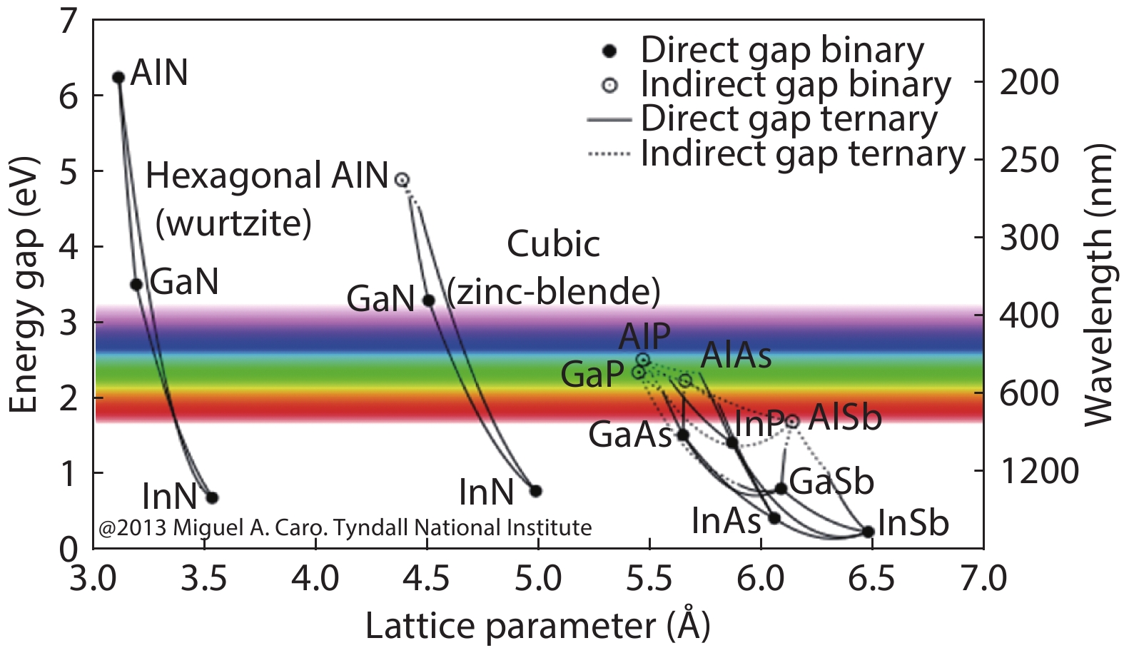
Fig. 1.
(Color online) The bandgap energy versus lattice constant of the III–V semiconductor material system. Reproduced with permission from Ref. [10]. Copyright 2013, Miguel ángel Caro Bayo.
REVIEWS
Chao Zhao1, 2, 3, 4, , Bo Xu3, 4, Zhijie Wang3, 4, and Zhanguo Wang3, 4
Corresponding author: Chao Zhao, E-mail: zhaochao83@gmail.com; Zhijie Wang, wangzj@semi.ac.cn
Abstract: Optoelectronic devices on silicon substrates are essential not only to the optoelectronic integrated circuit but also to low-cost lasers, large-area detectors, and so forth. Although heterogeneous integration of III–V semiconductors on Si has been well-developed, the thermal dissipation issue and the complicated fabrication process still hinders the development of these devices. The monolithic growth of III–V materials on Si has also been demonstrated by applying complicated buffer layers or interlayers. On the other hand, the growth of lattice-matched B-doped group-III–V materials is an attractive area of research. However, due to the difficulty in growth, the development is still relatively slow. Herein, we present a comprehensive review of the recent achievements in this field. We summarize and discuss the conditions and mechanisms involved in growing B-doped group-III–V materials. The unique surface morphology, crystallinity, and optical properties of the epitaxy correlating with their growth conditions are discussed, along with their respective optoelectronic applications. Finally, we detail the obstacles and challenges to exploit the potential for such practical applications fully.
Keywords: BGaAs, Si, photodetector, epitaxy
| [1] |
Janjua B, Ng T K, Zhao C, et al. True yellow light-emitting diodes as phosphor for tunable color-rendering index laser-based white light. ACS Photonics, 2016, 3, 2089 doi: 10.1021/acsphotonics.6b00457
|
| [2] |
Zhao C, Ng T K, Tseng C C, et al. InGaN/GaN nanowires epitaxy on large-area MoS2 for high-performance light-emitters. RSC Adv, 2017, 7, 26665 doi: 10.1039/C7RA03590J
|
| [3] |
Zhao C, Ebaid M, Zhang H, et al. Quantified hole concentration in AlGaN nanowires for high-performance ultraviolet emitters. Nanoscale, 2018, 10, 15980 doi: 10.1039/C8NR02615G
|
| [4] |
Zhao C, Alfaraj N, Subedi R C, et al. III-nitride nanowires on unconventional substrates: From materials to optoelectronic device applications. Prog Quantum Electron, 2018, 61, 1 doi: 10.1016/j.pquantelec.2018.07.001
|
| [5] |
Janjua B, Sun H, Zhao C, et al. Self-planarized quantum-disks-in-nanowires ultraviolet-B emitters utilizing pendeo-epitaxy. Nanoscale, 2017, 9, 7805 doi: 10.1039/C7NR00006E
|
| [6] |
Ebaid M, Priante D, Liu G, et al. Unbiased photocatalytic hydrogen generation from pure water on stable Ir-treated In0.33Ga0.67N nanorods. Nano Energy, 2017, 37, 158 doi: 10.1016/j.nanoen.2017.05.013
|
| [7] |
Zhao C, Chen Y H, Xu B, et al. Study of the wetting layer of InAs/GaAs nanorings grown by droplet epitaxy. Appl Phys Lett, 2008, 92, 063122 doi: 10.1063/1.2883931
|
| [8] |
Zhao C, Chen Y H, Xu B, et al. Evolution of InAs nanostructures grown by droplet epitaxy. Appl Phys Lett, 2007, 91, 033112 doi: 10.1063/1.2757151
|
| [9] |
Siddiqi G, Pan Z, Hu S. III–V semiconductor photoelectrodes. Semiconductors and Semimetals, 2017, 81
|
| [10] |
Caro Bayo M Á. Theory of elasticity and electric polarization effects in the group-III nitrides. PhD Dissertation, University College Cork, 2013
|
| [11] |
Roelkens G, Liu L, Liang D, et al. III–V/silicon photonics for on-chip and intra-chip optical interconnects. Laser Photonics Rev, 2010, 4, 751 doi: 10.1002/lpor.200900033
|
| [12] |
Chen S, Li W, Wu J, et al. Electrically pumped continuous-wave III–V quantum dot lasers on silicon. Nat Photonics, 2016, 10, 307 doi: 10.1038/nphoton.2016.21
|
| [13] |
Tischler M A, Mooney P M, Parker B D, et al. Metalorganic vapor phase epitaxy and characterization of boron-doped (Al,Ga)As. J Appl Phys, 1992, 71, 984 doi: 10.1063/1.351295
|
| [14] |
Geisz J F, Friedman D J, Kurtz S, et al. Epitaxial growth of BGaAs and BGaInAs by MOCVD. J Cryst Growth, 2001, 225, 372 doi: 10.1016/S0022-0248(01)00883-1
|
| [15] |
Hart G L W, Zunger A. Electronic structure of BAs and boride III–V alloys. Phys Rev B, 2000, 62, 13522 doi: 10.1103/PhysRevB.62.13522
|
| [16] |
Hoke W E. Molecular-beam epitaxial growth of boron-doped GaAs films. J Vac Sci Technol B, 1993, 11, 902 doi: 10.1116/1.586734
|
| [17] |
Gupta V K, Koch M W, Watkins N J, et al. Molecular beam epitaxial growth of BGaAs ternary compounds. J Electron Mater, 2000, 29, 1387 doi: 10.1007/s11664-000-0123-3
|
| [18] |
Tian F, Song B, Chen X, et al. Unusual high thermal conductivity in boron arsenide bulk crystals. Science, 2018, 361, 582 doi: 10.1126/science.aat7932
|
| [19] |
Li S, Zheng Q, Lv Y, et al. High thermal conductivity in cubic boron arsenide crystals. Science, 2018, 361, 579 doi: 10.1126/science.aat8982
|
| [20] |
Kang J S, Li M, Wu H, et al. Experimental observation of high thermal conductivity in boron arsenide. Science, 2018, 361, 575 doi: 10.1126/science.aat5522
|
| [21] |
Detz H, MacFarland D, Zederbauer T, et al. Growth rate dependence of boron incorporation into BxGa1− xAs layers. J Cryst Growth, 2017, 477, 77 doi: 10.1016/j.jcrysgro.2017.02.043
|
| [22] |
Dumont H, Rutzinger D, Vincent C, et al. Surface segregation of boron in BxGa1− xAs/GaAs epilayers studied by X-ray photoelectron spectroscopy and atomic force microscopy. Appl Phys Lett, 2003, 82, 1830 doi: 10.1063/1.1561164
|
| [23] |
Azzi S, Zaoui A, Ferhat M. On the importance of the band gap bowing in boron-based III–V ternary alloys. Solid State Commun, 2007, 144, 245 doi: 10.1016/j.ssc.2007.08.017
|
| [24] |
Pryakhin D A. Growth of BGaAs layers on GaAs substrates by metal–organic vapor-phase epitaxy. Semiconductors, 2005, 39, 11 doi: 10.1134/1.1852634
|
| [25] |
Dumont H, Dazord J, Monteil Y, et al. Growth and characterization of high quality BxGa1− xAs/GaAs(001) epilayers. J Cryst Growth, 2003, 248, 463 doi: 10.1016/S0022-0248(02)01822-5
|
| [26] |
El-Jaroudi R H, McNicholas K M, Bouslog B A, et al. Boron alloys for GaAs-based 1.3 μm semiconductor lasers. Conference on Lasers and Electro-Optics, 2019
|
| [27] |
Geisz J F, Friedman D J, Olson J M, et al. BGaInAs alloys lattice matched to GaAs. Appl Phys Lett, 2000, 76, 1443 doi: 10.1063/1.126058
|
| [28] |
Geisz J F, Friedman D J, Kurtz S, et al. Alternative boron precursors for BGaAs epitaxy. J Electron Mater, 2001, 30, 1387 doi: 10.1007/s11664-001-0188-7
|
| [29] |
Beaton D A, Ptak A J, Alberi K, et al. Quaternary bismide alloy lattice matched to GaAs. J Cryst Growth, 2012, 351, 37 doi: 10.1016/j.jcrysgro.2012.04.028
|
| [30] |
Ptak A J, Beaton D A, Mascarenhas A. Growth of BGaAs by molecular-beam epitaxy and the effects of a bismuth surfactant. J Cryst Growth, 2012, 351, 122 doi: 10.1016/j.jcrysgro.2012.04.026
|
| [31] |
Dumont H, Monteil Y. Some aspects on thermodynamic properties, phase diagram and alloy formation in the ternary system BAs–GaAs—Part II: BGaAs alloy formation. J Cryst Growth, 2006, 290, 419 doi: 10.1016/j.jcrysgro.2005.12.080
|
| [32] |
Saidi F, Hassen F, Maaref H, et al. Optical study of BxGa1− xAs/GaAs epilayers. Mater Sci Engi C, 2006, 26, 236 doi: 10.1016/j.msec.2005.10.056
|
| [33] |
Saidi F, Hassen F, Dumont H, et al. Comparative optical study of GaAs1− xNx/GaAs and BxGa1− xAs/GaAs epilayers. IEE Proc - Optoelectron, 2004, 151, 342 doi: 10.1049/ip-opt:20040938
|
| [34] |
Wang Q, Jia Z, Ren X, et al. Effect of boron incorporation on the structural and photoluminescence properties of highly-strained InxGa1− xAs/GaAs multiple quantum wells. AIP Adv, 2013, 3, 072111 doi: 10.1063/1.4815971
|
| [35] |
Hamila R, Saidi F, Fouzri A, et al. Clustering effects in optical properties of BGaAs/GaAs epilayers. J Lumin, 2009, 129, 1010 doi: 10.1016/j.jlumin.2009.04.013
|
| [36] |
Hamila R, Saidi F, Rodriguez P H, et al. Growth temperature effects on boron incorporation and optical properties of BGaAs/GaAs grown by MOCVD. J Alloys Compnd, 2010, 506, 10 doi: 10.1016/j.jallcom.2010.06.169
|
| [37] |
Saidi F, Hamila R, Maaref H, et al. Structural and optical study of BxInyGa1− x− yAs/GaAs and InyGa1− yAs/GaAs QW’s grown by MOCVD. J Alloys Compnd, 2010, 491, 45 doi: 10.1016/j.jallcom.2009.10.244
|
| [38] |
Rodriguez P, Auvray L, Dumont H, et al. Growth and characterization of BGaAs and BInGaAs epilayers on GaAs by MOVPE. J Cryst Growth, 2007, 298, 81 doi: 10.1016/j.jcrysgro.2006.10.118
|
| [39] |
Hamila R, Saidi F, Maaref H, et al. Photoluminescence properties and high resolution X-ray diffraction investigation of BInGaAs/GaAs grown by the metalorganic vapour phase epitaxy method. J Appl Phys, 2012, 112, 063109 doi: 10.1063/1.4752031
|
| [40] |
Hamila R, Saidi F, Rodriguez P, et al. Structural and optical study of BInGaAs/GaAs quantum wells grown by MOVPE emitting above 1.1 eV. Microelectron Eng, 2016, 149, 5 doi: 10.1016/j.mee.2015.08.013
|
| [41] |
Hidouri T, Saidi F, Maaref H, et al. Localized state exciton model investigation of B-content effect on optical properties of BGaAs/GaAs epilayers grown by MOCVD. Vacuum, 2016, 132, 10 doi: 10.1016/j.vacuum.2016.07.018
|
| [42] |
Hidouri T, Saidi F, Maaref H, et al. LSE investigation of the thermal effect on band gap energy and thermodynamic parameters of BInGaAs/GaAs single quantum well. Opt Mater, 2016, 62, 267 doi: 10.1016/j.optmat.2016.10.010
|
| [43] |
Hidouri T, Saidi F, Maaref H, et al. Impact of photoluminescence temperature and growth parameter on the exciton localized in BxGa1-xAs/GaAs epilayers grown by MOCVD. Opt Mater, 2016, 60, 487 doi: 10.1016/j.optmat.2016.08.029
|
| [44] |
Rodriguez P, Auvray L, Favier A, et al. Influence of boron surface enrichment on the growth mode of BGaAs epilayers grown on GaAs by metalorganic vapour phase epitaxy. Thin Solid Films, 2008, 516, 8424 doi: 10.1016/j.tsf.2008.04.053
|
| [45] |
Ilahi S, Baira M, Saidi F, et al. Non-radiative recombination process in BGaAs/GaAs alloys: Two layer photothermal deflection model. J Alloys Compnd, 2013, 581, 358 doi: 10.1016/j.jallcom.2013.07.101
|
| [46] |
Ilahi S, Saidi F, Hamila R, et al. Photothermal deflection spectroscopy PDS investigation of optical and thermal properties of BGaAs/GaAs alloys. Curr Appl Phys, 2013, 13, 610 doi: 10.1016/j.cap.2012.11.002
|
| [47] |
Ilahi S, Saidi F, Hamila R, et al. Shift of the gap energy and thermal conductivity in BGaAs/GaAs alloys. Physica B, 2013, 421, 105 doi: 10.1016/j.physb.2013.03.045
|
| [48] |
Wang Q, Ren X, Wang F, et al. LP-MOCVD growth of ternary BxGa1− xAs epilayers on (001)GaAs substrates using TEB, TMGa and AsH3. Microelectron J, 2008, 39, 1678 doi: 10.1016/j.mejo.2008.02.017
|
| [49] |
Wang Q, Ren X, Huang H, et al. Growth of BxGa1− xAs, BxAl1− xAs and BxGa1− x− yInyAs epilayers on (001) GaAs by low pressure metalorganic chemical vapor deposition. Microelectron J, 2009, 40, 87 doi: 10.1016/j.mejo.2008.06.066
|
| [50] |
Lancaster S, Groiss H, Zederbauer T, et al. Suppression of axial growth by boron incorporation in GaAs nanowires grown by self-catalyzed molecular beam epitaxy. Nanotechnology, 2019, 30, 065602 doi: 10.1088/1361-6528/aaf11e
|
| [51] |
Brierley S K, Hendriks H T, Hoke W E, et al. Observation of boron-related photoluminescence in GaAs layers grown by molecular beam epitaxy. Appl Phys Lett, 1993, 63, 812 doi: 10.1063/1.109916
|
| [52] |
Kley A, Ruggerone P, Scheffler M. Novel diffusion mechanism on the GaAs (001) surface: the role of adatom-dimer interaction. Phys Rev Letters, 1997, 79, 5278 doi: 10.1103/PhysRevLett.79.5278
|
| [53] |
Paulus B, Fulde P, Stoll H. Cohesive energies of cubic III-V semiconductors. Phys Rev B, 1996, 54, 2556 doi: 10.1103/PhysRevB.54.2556
|
| [54] |
Groenert M E, Averbeck R, Hösler W, et al. Optimized growth of BGaAs by molecular beam epitaxy. J Cryst Growth, 2004, 264, 123 doi: 10.1016/j.jcrysgro.2004.01.010
|
| [55] |
Lancaster S, Andrews A M, Stoeger-Pollach M, et al. Influence of boron antisite defects on the electrical properties of MBE-grown GaAs nanowires. Phys Status Solidi B, 2019, 256, 1800368 doi: 10.1002/pssb.201800368
|
| [56] |
Bank S R, McNicholas K M, El-Jaroudi R H, et al. Improved MWIR LED arrays on Si substrates for scene projectors. IEEE Research and Applications of Photonics In Defense Conference (RAPID), 2018
|
| [57] |
Lindsay A, O’Reilly E P. Theory of electronic structure of BGaAs and related alloys. Phys Status Solidi C, 2008, 5, 454 doi: 10.1002/pssc.200777456
|
| [58] |
Sommer N, Buss R, Ohlmann J, et al. Growth of (BGa)As, (BGa)P, (BGa)(AsP) and (BGaIn)P by MOVPE. J Cryst Growth, 2013, 370, 191 doi: 10.1016/j.jcrysgro.2012.07.035
|
| [59] |
Zhang S B, Zunger A. Surface-reconstruction-enhanced solubility of N, P, As, and Sb in III–V semiconductors. Appl Phys Lett, 1997, 71, 677 doi: 10.1063/1.119827
|
| [60] |
Jenichen A, Engler C. Stability and band gaps of InGaAs, BGaAs, and BInGaAs alloys: Density-functional supercell calculations. Phys Status Solidi B, 2007, 244, 1957 doi: 10.1002/pssb.200642215
|
| [61] |
Jenichen A, Engler C. Boron and indium substitution in GaAs (001) surfaces: Density-functional supercell calculations of the surface stability. Surf Sci, 2007, 601, 900 doi: 10.1016/j.susc.2006.11.043
|
| [62] |
Jenichen A, Engler C. Metalorganic chemical-vapour-deposition (MOCVD) of InGaAs, BGaAs, and BInGaAs: Quantum chemical calculations on the mechanisms. J Cryst Growth, 2007, 304, 26 doi: 10.1016/j.jcrysgro.2007.02.019
|
Table 1. Calculated bowing btot as well as its three contributions in eV. Reproduced with permission from Ref. [23]. Copyright 2007, Elsevier.
| System | bVD | bCE | bSR | btot | bthe | bexp |
| Mixed cation | ||||||
| BAlN | 4.88 | 1.62 | –1.05 | 5.45 | ||
| BGaN | 7.47 | 1.47 | –1.66 | 7.28 | 4.3 (x = 0.6) | |
| BInN | 14.73 | 2.03 | –3.29 | 13.48 | ||
| BAlP | 4.41 | 1.20 | –0.95 | 4.65 | ||
| BGaP | 4.61 | 1.04 | –1.00 | 4.65 | ||
| BInP | 8.74 | 1.61 | –1.92 | 8.43 | ||
| BAlAs | 2.77 | 1.17 | –0.59 | 3.35 | ||
| BGaAs | 3.03 | 1.02 | –0.66 | 3.39 | 3.5 (x < 0.6) | 2.3 (x < 0.4) |
| BInAs | 6.08 | 1.58 | –1.34 | 6.32 | ||
| BAlSb | 0.15 | 1.07 | –0.03 | 1.18 | ||
| BGaSb | –0.17 | 0.92 | –0.09 | 0.65 | ||
| BInSb | 0.70 | 1.48 | –0.08 | 2.10 | ||
| Mixed anion | ||||||
| BNP | 2.10 | 1.94 | 3.89 | 7.94 | 9.92 | |
| BNAs | 5.13 | 2.29 | 4.87 | 12.30 | 9.33 | |
| BNSb | 14.30 | 3.52 | 1.96 | 19.78 | 10.27, 21.19 | |
| BPSb | 4.48 | 0.56 | 1.76 | 6.80 | 0.038 | |
| BPAs | 0.52 | 0.34 | 0.00 | 0.87 | –0.06 | |
| BAsSb | 1.94 | 0.47 | 1.10 | 3.50 | 0.10 |
 DownLoad: CSV
| [1] |
Janjua B, Ng T K, Zhao C, et al. True yellow light-emitting diodes as phosphor for tunable color-rendering index laser-based white light. ACS Photonics, 2016, 3, 2089 doi: 10.1021/acsphotonics.6b00457
|
| [2] |
Zhao C, Ng T K, Tseng C C, et al. InGaN/GaN nanowires epitaxy on large-area MoS2 for high-performance light-emitters. RSC Adv, 2017, 7, 26665 doi: 10.1039/C7RA03590J
|
| [3] |
Zhao C, Ebaid M, Zhang H, et al. Quantified hole concentration in AlGaN nanowires for high-performance ultraviolet emitters. Nanoscale, 2018, 10, 15980 doi: 10.1039/C8NR02615G
|
| [4] |
Zhao C, Alfaraj N, Subedi R C, et al. III-nitride nanowires on unconventional substrates: From materials to optoelectronic device applications. Prog Quantum Electron, 2018, 61, 1 doi: 10.1016/j.pquantelec.2018.07.001
|
| [5] |
Janjua B, Sun H, Zhao C, et al. Self-planarized quantum-disks-in-nanowires ultraviolet-B emitters utilizing pendeo-epitaxy. Nanoscale, 2017, 9, 7805 doi: 10.1039/C7NR00006E
|
| [6] |
Ebaid M, Priante D, Liu G, et al. Unbiased photocatalytic hydrogen generation from pure water on stable Ir-treated In0.33Ga0.67N nanorods. Nano Energy, 2017, 37, 158 doi: 10.1016/j.nanoen.2017.05.013
|
| [7] |
Zhao C, Chen Y H, Xu B, et al. Study of the wetting layer of InAs/GaAs nanorings grown by droplet epitaxy. Appl Phys Lett, 2008, 92, 063122 doi: 10.1063/1.2883931
|
| [8] |
Zhao C, Chen Y H, Xu B, et al. Evolution of InAs nanostructures grown by droplet epitaxy. Appl Phys Lett, 2007, 91, 033112 doi: 10.1063/1.2757151
|
| [9] |
Siddiqi G, Pan Z, Hu S. III–V semiconductor photoelectrodes. Semiconductors and Semimetals, 2017, 81
|
| [10] |
Caro Bayo M Á. Theory of elasticity and electric polarization effects in the group-III nitrides. PhD Dissertation, University College Cork, 2013
|
| [11] |
Roelkens G, Liu L, Liang D, et al. III–V/silicon photonics for on-chip and intra-chip optical interconnects. Laser Photonics Rev, 2010, 4, 751 doi: 10.1002/lpor.200900033
|
| [12] |
Chen S, Li W, Wu J, et al. Electrically pumped continuous-wave III–V quantum dot lasers on silicon. Nat Photonics, 2016, 10, 307 doi: 10.1038/nphoton.2016.21
|
| [13] |
Tischler M A, Mooney P M, Parker B D, et al. Metalorganic vapor phase epitaxy and characterization of boron-doped (Al,Ga)As. J Appl Phys, 1992, 71, 984 doi: 10.1063/1.351295
|
| [14] |
Geisz J F, Friedman D J, Kurtz S, et al. Epitaxial growth of BGaAs and BGaInAs by MOCVD. J Cryst Growth, 2001, 225, 372 doi: 10.1016/S0022-0248(01)00883-1
|
| [15] |
Hart G L W, Zunger A. Electronic structure of BAs and boride III–V alloys. Phys Rev B, 2000, 62, 13522 doi: 10.1103/PhysRevB.62.13522
|
| [16] |
Hoke W E. Molecular-beam epitaxial growth of boron-doped GaAs films. J Vac Sci Technol B, 1993, 11, 902 doi: 10.1116/1.586734
|
| [17] |
Gupta V K, Koch M W, Watkins N J, et al. Molecular beam epitaxial growth of BGaAs ternary compounds. J Electron Mater, 2000, 29, 1387 doi: 10.1007/s11664-000-0123-3
|
| [18] |
Tian F, Song B, Chen X, et al. Unusual high thermal conductivity in boron arsenide bulk crystals. Science, 2018, 361, 582 doi: 10.1126/science.aat7932
|
| [19] |
Li S, Zheng Q, Lv Y, et al. High thermal conductivity in cubic boron arsenide crystals. Science, 2018, 361, 579 doi: 10.1126/science.aat8982
|
| [20] |
Kang J S, Li M, Wu H, et al. Experimental observation of high thermal conductivity in boron arsenide. Science, 2018, 361, 575 doi: 10.1126/science.aat5522
|
| [21] |
Detz H, MacFarland D, Zederbauer T, et al. Growth rate dependence of boron incorporation into BxGa1− xAs layers. J Cryst Growth, 2017, 477, 77 doi: 10.1016/j.jcrysgro.2017.02.043
|
| [22] |
Dumont H, Rutzinger D, Vincent C, et al. Surface segregation of boron in BxGa1− xAs/GaAs epilayers studied by X-ray photoelectron spectroscopy and atomic force microscopy. Appl Phys Lett, 2003, 82, 1830 doi: 10.1063/1.1561164
|
| [23] |
Azzi S, Zaoui A, Ferhat M. On the importance of the band gap bowing in boron-based III–V ternary alloys. Solid State Commun, 2007, 144, 245 doi: 10.1016/j.ssc.2007.08.017
|
| [24] |
Pryakhin D A. Growth of BGaAs layers on GaAs substrates by metal–organic vapor-phase epitaxy. Semiconductors, 2005, 39, 11 doi: 10.1134/1.1852634
|
| [25] |
Dumont H, Dazord J, Monteil Y, et al. Growth and characterization of high quality BxGa1− xAs/GaAs(001) epilayers. J Cryst Growth, 2003, 248, 463 doi: 10.1016/S0022-0248(02)01822-5
|
| [26] |
El-Jaroudi R H, McNicholas K M, Bouslog B A, et al. Boron alloys for GaAs-based 1.3 μm semiconductor lasers. Conference on Lasers and Electro-Optics, 2019
|
| [27] |
Geisz J F, Friedman D J, Olson J M, et al. BGaInAs alloys lattice matched to GaAs. Appl Phys Lett, 2000, 76, 1443 doi: 10.1063/1.126058
|
| [28] |
Geisz J F, Friedman D J, Kurtz S, et al. Alternative boron precursors for BGaAs epitaxy. J Electron Mater, 2001, 30, 1387 doi: 10.1007/s11664-001-0188-7
|
| [29] |
Beaton D A, Ptak A J, Alberi K, et al. Quaternary bismide alloy lattice matched to GaAs. J Cryst Growth, 2012, 351, 37 doi: 10.1016/j.jcrysgro.2012.04.028
|
| [30] |
Ptak A J, Beaton D A, Mascarenhas A. Growth of BGaAs by molecular-beam epitaxy and the effects of a bismuth surfactant. J Cryst Growth, 2012, 351, 122 doi: 10.1016/j.jcrysgro.2012.04.026
|
| [31] |
Dumont H, Monteil Y. Some aspects on thermodynamic properties, phase diagram and alloy formation in the ternary system BAs–GaAs—Part II: BGaAs alloy formation. J Cryst Growth, 2006, 290, 419 doi: 10.1016/j.jcrysgro.2005.12.080
|
| [32] |
Saidi F, Hassen F, Maaref H, et al. Optical study of BxGa1− xAs/GaAs epilayers. Mater Sci Engi C, 2006, 26, 236 doi: 10.1016/j.msec.2005.10.056
|
| [33] |
Saidi F, Hassen F, Dumont H, et al. Comparative optical study of GaAs1− xNx/GaAs and BxGa1− xAs/GaAs epilayers. IEE Proc - Optoelectron, 2004, 151, 342 doi: 10.1049/ip-opt:20040938
|
| [34] |
Wang Q, Jia Z, Ren X, et al. Effect of boron incorporation on the structural and photoluminescence properties of highly-strained InxGa1− xAs/GaAs multiple quantum wells. AIP Adv, 2013, 3, 072111 doi: 10.1063/1.4815971
|
| [35] |
Hamila R, Saidi F, Fouzri A, et al. Clustering effects in optical properties of BGaAs/GaAs epilayers. J Lumin, 2009, 129, 1010 doi: 10.1016/j.jlumin.2009.04.013
|
| [36] |
Hamila R, Saidi F, Rodriguez P H, et al. Growth temperature effects on boron incorporation and optical properties of BGaAs/GaAs grown by MOCVD. J Alloys Compnd, 2010, 506, 10 doi: 10.1016/j.jallcom.2010.06.169
|
| [37] |
Saidi F, Hamila R, Maaref H, et al. Structural and optical study of BxInyGa1− x− yAs/GaAs and InyGa1− yAs/GaAs QW’s grown by MOCVD. J Alloys Compnd, 2010, 491, 45 doi: 10.1016/j.jallcom.2009.10.244
|
| [38] |
Rodriguez P, Auvray L, Dumont H, et al. Growth and characterization of BGaAs and BInGaAs epilayers on GaAs by MOVPE. J Cryst Growth, 2007, 298, 81 doi: 10.1016/j.jcrysgro.2006.10.118
|
| [39] |
Hamila R, Saidi F, Maaref H, et al. Photoluminescence properties and high resolution X-ray diffraction investigation of BInGaAs/GaAs grown by the metalorganic vapour phase epitaxy method. J Appl Phys, 2012, 112, 063109 doi: 10.1063/1.4752031
|
| [40] |
Hamila R, Saidi F, Rodriguez P, et al. Structural and optical study of BInGaAs/GaAs quantum wells grown by MOVPE emitting above 1.1 eV. Microelectron Eng, 2016, 149, 5 doi: 10.1016/j.mee.2015.08.013
|
| [41] |
Hidouri T, Saidi F, Maaref H, et al. Localized state exciton model investigation of B-content effect on optical properties of BGaAs/GaAs epilayers grown by MOCVD. Vacuum, 2016, 132, 10 doi: 10.1016/j.vacuum.2016.07.018
|
| [42] |
Hidouri T, Saidi F, Maaref H, et al. LSE investigation of the thermal effect on band gap energy and thermodynamic parameters of BInGaAs/GaAs single quantum well. Opt Mater, 2016, 62, 267 doi: 10.1016/j.optmat.2016.10.010
|
| [43] |
Hidouri T, Saidi F, Maaref H, et al. Impact of photoluminescence temperature and growth parameter on the exciton localized in BxGa1-xAs/GaAs epilayers grown by MOCVD. Opt Mater, 2016, 60, 487 doi: 10.1016/j.optmat.2016.08.029
|
| [44] |
Rodriguez P, Auvray L, Favier A, et al. Influence of boron surface enrichment on the growth mode of BGaAs epilayers grown on GaAs by metalorganic vapour phase epitaxy. Thin Solid Films, 2008, 516, 8424 doi: 10.1016/j.tsf.2008.04.053
|
| [45] |
Ilahi S, Baira M, Saidi F, et al. Non-radiative recombination process in BGaAs/GaAs alloys: Two layer photothermal deflection model. J Alloys Compnd, 2013, 581, 358 doi: 10.1016/j.jallcom.2013.07.101
|
| [46] |
Ilahi S, Saidi F, Hamila R, et al. Photothermal deflection spectroscopy PDS investigation of optical and thermal properties of BGaAs/GaAs alloys. Curr Appl Phys, 2013, 13, 610 doi: 10.1016/j.cap.2012.11.002
|
| [47] |
Ilahi S, Saidi F, Hamila R, et al. Shift of the gap energy and thermal conductivity in BGaAs/GaAs alloys. Physica B, 2013, 421, 105 doi: 10.1016/j.physb.2013.03.045
|
| [48] |
Wang Q, Ren X, Wang F, et al. LP-MOCVD growth of ternary BxGa1− xAs epilayers on (001)GaAs substrates using TEB, TMGa and AsH3. Microelectron J, 2008, 39, 1678 doi: 10.1016/j.mejo.2008.02.017
|
| [49] |
Wang Q, Ren X, Huang H, et al. Growth of BxGa1− xAs, BxAl1− xAs and BxGa1− x− yInyAs epilayers on (001) GaAs by low pressure metalorganic chemical vapor deposition. Microelectron J, 2009, 40, 87 doi: 10.1016/j.mejo.2008.06.066
|
| [50] |
Lancaster S, Groiss H, Zederbauer T, et al. Suppression of axial growth by boron incorporation in GaAs nanowires grown by self-catalyzed molecular beam epitaxy. Nanotechnology, 2019, 30, 065602 doi: 10.1088/1361-6528/aaf11e
|
| [51] |
Brierley S K, Hendriks H T, Hoke W E, et al. Observation of boron-related photoluminescence in GaAs layers grown by molecular beam epitaxy. Appl Phys Lett, 1993, 63, 812 doi: 10.1063/1.109916
|
| [52] |
Kley A, Ruggerone P, Scheffler M. Novel diffusion mechanism on the GaAs (001) surface: the role of adatom-dimer interaction. Phys Rev Letters, 1997, 79, 5278 doi: 10.1103/PhysRevLett.79.5278
|
| [53] |
Paulus B, Fulde P, Stoll H. Cohesive energies of cubic III-V semiconductors. Phys Rev B, 1996, 54, 2556 doi: 10.1103/PhysRevB.54.2556
|
| [54] |
Groenert M E, Averbeck R, Hösler W, et al. Optimized growth of BGaAs by molecular beam epitaxy. J Cryst Growth, 2004, 264, 123 doi: 10.1016/j.jcrysgro.2004.01.010
|
| [55] |
Lancaster S, Andrews A M, Stoeger-Pollach M, et al. Influence of boron antisite defects on the electrical properties of MBE-grown GaAs nanowires. Phys Status Solidi B, 2019, 256, 1800368 doi: 10.1002/pssb.201800368
|
| [56] |
Bank S R, McNicholas K M, El-Jaroudi R H, et al. Improved MWIR LED arrays on Si substrates for scene projectors. IEEE Research and Applications of Photonics In Defense Conference (RAPID), 2018
|
| [57] |
Lindsay A, O’Reilly E P. Theory of electronic structure of BGaAs and related alloys. Phys Status Solidi C, 2008, 5, 454 doi: 10.1002/pssc.200777456
|
| [58] |
Sommer N, Buss R, Ohlmann J, et al. Growth of (BGa)As, (BGa)P, (BGa)(AsP) and (BGaIn)P by MOVPE. J Cryst Growth, 2013, 370, 191 doi: 10.1016/j.jcrysgro.2012.07.035
|
| [59] |
Zhang S B, Zunger A. Surface-reconstruction-enhanced solubility of N, P, As, and Sb in III–V semiconductors. Appl Phys Lett, 1997, 71, 677 doi: 10.1063/1.119827
|
| [60] |
Jenichen A, Engler C. Stability and band gaps of InGaAs, BGaAs, and BInGaAs alloys: Density-functional supercell calculations. Phys Status Solidi B, 2007, 244, 1957 doi: 10.1002/pssb.200642215
|
| [61] |
Jenichen A, Engler C. Boron and indium substitution in GaAs (001) surfaces: Density-functional supercell calculations of the surface stability. Surf Sci, 2007, 601, 900 doi: 10.1016/j.susc.2006.11.043
|
| [62] |
Jenichen A, Engler C. Metalorganic chemical-vapour-deposition (MOCVD) of InGaAs, BGaAs, and BInGaAs: Quantum chemical calculations on the mechanisms. J Cryst Growth, 2007, 304, 26 doi: 10.1016/j.jcrysgro.2007.02.019
|


Article views: 7053 Times PDF downloads: 307 Times Cited by: 0 Times
Received: 07 November 2019 Revised: Online: Accepted Manuscript: 06 December 2019Uncorrected proof: 13 December 2019Published: 02 January 2020
| Citation: |
Chao Zhao, Bo Xu, Zhijie Wang, Zhanguo Wang. Boron-doped III–V semiconductors for Si-based optoelectronic devices[J]. Journal of Semiconductors, 2020, 41(1): 011301. doi: 10.1088/1674-4926/41/1/011301
****
C Zhao, B Xu, Z J Wang, Z G Wang, Boron-doped III–V semiconductors for Si-based optoelectronic devices[J]. J. Semicond., 2020, 41(1): 011301. doi: 10.1088/1674-4926/41/1/011301.

|
| [1] |
Janjua B, Ng T K, Zhao C, et al. True yellow light-emitting diodes as phosphor for tunable color-rendering index laser-based white light. ACS Photonics, 2016, 3, 2089 doi: 10.1021/acsphotonics.6b00457
|
| [2] |
Zhao C, Ng T K, Tseng C C, et al. InGaN/GaN nanowires epitaxy on large-area MoS2 for high-performance light-emitters. RSC Adv, 2017, 7, 26665 doi: 10.1039/C7RA03590J
|
| [3] |
Zhao C, Ebaid M, Zhang H, et al. Quantified hole concentration in AlGaN nanowires for high-performance ultraviolet emitters. Nanoscale, 2018, 10, 15980 doi: 10.1039/C8NR02615G
|
| [4] |
Zhao C, Alfaraj N, Subedi R C, et al. III-nitride nanowires on unconventional substrates: From materials to optoelectronic device applications. Prog Quantum Electron, 2018, 61, 1 doi: 10.1016/j.pquantelec.2018.07.001
|
| [5] |
Janjua B, Sun H, Zhao C, et al. Self-planarized quantum-disks-in-nanowires ultraviolet-B emitters utilizing pendeo-epitaxy. Nanoscale, 2017, 9, 7805 doi: 10.1039/C7NR00006E
|
| [6] |
Ebaid M, Priante D, Liu G, et al. Unbiased photocatalytic hydrogen generation from pure water on stable Ir-treated In0.33Ga0.67N nanorods. Nano Energy, 2017, 37, 158 doi: 10.1016/j.nanoen.2017.05.013
|
| [7] |
Zhao C, Chen Y H, Xu B, et al. Study of the wetting layer of InAs/GaAs nanorings grown by droplet epitaxy. Appl Phys Lett, 2008, 92, 063122 doi: 10.1063/1.2883931
|
| [8] |
Zhao C, Chen Y H, Xu B, et al. Evolution of InAs nanostructures grown by droplet epitaxy. Appl Phys Lett, 2007, 91, 033112 doi: 10.1063/1.2757151
|
| [9] |
Siddiqi G, Pan Z, Hu S. III–V semiconductor photoelectrodes. Semiconductors and Semimetals, 2017, 81
|
| [10] |
Caro Bayo M Á. Theory of elasticity and electric polarization effects in the group-III nitrides. PhD Dissertation, University College Cork, 2013
|
| [11] |
Roelkens G, Liu L, Liang D, et al. III–V/silicon photonics for on-chip and intra-chip optical interconnects. Laser Photonics Rev, 2010, 4, 751 doi: 10.1002/lpor.200900033
|
| [12] |
Chen S, Li W, Wu J, et al. Electrically pumped continuous-wave III–V quantum dot lasers on silicon. Nat Photonics, 2016, 10, 307 doi: 10.1038/nphoton.2016.21
|
| [13] |
Tischler M A, Mooney P M, Parker B D, et al. Metalorganic vapor phase epitaxy and characterization of boron-doped (Al,Ga)As. J Appl Phys, 1992, 71, 984 doi: 10.1063/1.351295
|
| [14] |
Geisz J F, Friedman D J, Kurtz S, et al. Epitaxial growth of BGaAs and BGaInAs by MOCVD. J Cryst Growth, 2001, 225, 372 doi: 10.1016/S0022-0248(01)00883-1
|
| [15] |
Hart G L W, Zunger A. Electronic structure of BAs and boride III–V alloys. Phys Rev B, 2000, 62, 13522 doi: 10.1103/PhysRevB.62.13522
|
| [16] |
Hoke W E. Molecular-beam epitaxial growth of boron-doped GaAs films. J Vac Sci Technol B, 1993, 11, 902 doi: 10.1116/1.586734
|
| [17] |
Gupta V K, Koch M W, Watkins N J, et al. Molecular beam epitaxial growth of BGaAs ternary compounds. J Electron Mater, 2000, 29, 1387 doi: 10.1007/s11664-000-0123-3
|
| [18] |
Tian F, Song B, Chen X, et al. Unusual high thermal conductivity in boron arsenide bulk crystals. Science, 2018, 361, 582 doi: 10.1126/science.aat7932
|
| [19] |
Li S, Zheng Q, Lv Y, et al. High thermal conductivity in cubic boron arsenide crystals. Science, 2018, 361, 579 doi: 10.1126/science.aat8982
|
| [20] |
Kang J S, Li M, Wu H, et al. Experimental observation of high thermal conductivity in boron arsenide. Science, 2018, 361, 575 doi: 10.1126/science.aat5522
|
| [21] |
Detz H, MacFarland D, Zederbauer T, et al. Growth rate dependence of boron incorporation into BxGa1− xAs layers. J Cryst Growth, 2017, 477, 77 doi: 10.1016/j.jcrysgro.2017.02.043
|
| [22] |
Dumont H, Rutzinger D, Vincent C, et al. Surface segregation of boron in BxGa1− xAs/GaAs epilayers studied by X-ray photoelectron spectroscopy and atomic force microscopy. Appl Phys Lett, 2003, 82, 1830 doi: 10.1063/1.1561164
|
| [23] |
Azzi S, Zaoui A, Ferhat M. On the importance of the band gap bowing in boron-based III–V ternary alloys. Solid State Commun, 2007, 144, 245 doi: 10.1016/j.ssc.2007.08.017
|
| [24] |
Pryakhin D A. Growth of BGaAs layers on GaAs substrates by metal–organic vapor-phase epitaxy. Semiconductors, 2005, 39, 11 doi: 10.1134/1.1852634
|
| [25] |
Dumont H, Dazord J, Monteil Y, et al. Growth and characterization of high quality BxGa1− xAs/GaAs(001) epilayers. J Cryst Growth, 2003, 248, 463 doi: 10.1016/S0022-0248(02)01822-5
|
| [26] |
El-Jaroudi R H, McNicholas K M, Bouslog B A, et al. Boron alloys for GaAs-based 1.3 μm semiconductor lasers. Conference on Lasers and Electro-Optics, 2019
|
| [27] |
Geisz J F, Friedman D J, Olson J M, et al. BGaInAs alloys lattice matched to GaAs. Appl Phys Lett, 2000, 76, 1443 doi: 10.1063/1.126058
|
| [28] |
Geisz J F, Friedman D J, Kurtz S, et al. Alternative boron precursors for BGaAs epitaxy. J Electron Mater, 2001, 30, 1387 doi: 10.1007/s11664-001-0188-7
|
| [29] |
Beaton D A, Ptak A J, Alberi K, et al. Quaternary bismide alloy lattice matched to GaAs. J Cryst Growth, 2012, 351, 37 doi: 10.1016/j.jcrysgro.2012.04.028
|
| [30] |
Ptak A J, Beaton D A, Mascarenhas A. Growth of BGaAs by molecular-beam epitaxy and the effects of a bismuth surfactant. J Cryst Growth, 2012, 351, 122 doi: 10.1016/j.jcrysgro.2012.04.026
|
| [31] |
Dumont H, Monteil Y. Some aspects on thermodynamic properties, phase diagram and alloy formation in the ternary system BAs–GaAs—Part II: BGaAs alloy formation. J Cryst Growth, 2006, 290, 419 doi: 10.1016/j.jcrysgro.2005.12.080
|
| [32] |
Saidi F, Hassen F, Maaref H, et al. Optical study of BxGa1− xAs/GaAs epilayers. Mater Sci Engi C, 2006, 26, 236 doi: 10.1016/j.msec.2005.10.056
|
| [33] |
Saidi F, Hassen F, Dumont H, et al. Comparative optical study of GaAs1− xNx/GaAs and BxGa1− xAs/GaAs epilayers. IEE Proc - Optoelectron, 2004, 151, 342 doi: 10.1049/ip-opt:20040938
|
| [34] |
Wang Q, Jia Z, Ren X, et al. Effect of boron incorporation on the structural and photoluminescence properties of highly-strained InxGa1− xAs/GaAs multiple quantum wells. AIP Adv, 2013, 3, 072111 doi: 10.1063/1.4815971
|
| [35] |
Hamila R, Saidi F, Fouzri A, et al. Clustering effects in optical properties of BGaAs/GaAs epilayers. J Lumin, 2009, 129, 1010 doi: 10.1016/j.jlumin.2009.04.013
|
| [36] |
Hamila R, Saidi F, Rodriguez P H, et al. Growth temperature effects on boron incorporation and optical properties of BGaAs/GaAs grown by MOCVD. J Alloys Compnd, 2010, 506, 10 doi: 10.1016/j.jallcom.2010.06.169
|
| [37] |
Saidi F, Hamila R, Maaref H, et al. Structural and optical study of BxInyGa1− x− yAs/GaAs and InyGa1− yAs/GaAs QW’s grown by MOCVD. J Alloys Compnd, 2010, 491, 45 doi: 10.1016/j.jallcom.2009.10.244
|
| [38] |
Rodriguez P, Auvray L, Dumont H, et al. Growth and characterization of BGaAs and BInGaAs epilayers on GaAs by MOVPE. J Cryst Growth, 2007, 298, 81 doi: 10.1016/j.jcrysgro.2006.10.118
|
| [39] |
Hamila R, Saidi F, Maaref H, et al. Photoluminescence properties and high resolution X-ray diffraction investigation of BInGaAs/GaAs grown by the metalorganic vapour phase epitaxy method. J Appl Phys, 2012, 112, 063109 doi: 10.1063/1.4752031
|
| [40] |
Hamila R, Saidi F, Rodriguez P, et al. Structural and optical study of BInGaAs/GaAs quantum wells grown by MOVPE emitting above 1.1 eV. Microelectron Eng, 2016, 149, 5 doi: 10.1016/j.mee.2015.08.013
|
| [41] |
Hidouri T, Saidi F, Maaref H, et al. Localized state exciton model investigation of B-content effect on optical properties of BGaAs/GaAs epilayers grown by MOCVD. Vacuum, 2016, 132, 10 doi: 10.1016/j.vacuum.2016.07.018
|
| [42] |
Hidouri T, Saidi F, Maaref H, et al. LSE investigation of the thermal effect on band gap energy and thermodynamic parameters of BInGaAs/GaAs single quantum well. Opt Mater, 2016, 62, 267 doi: 10.1016/j.optmat.2016.10.010
|
| [43] |
Hidouri T, Saidi F, Maaref H, et al. Impact of photoluminescence temperature and growth parameter on the exciton localized in BxGa1-xAs/GaAs epilayers grown by MOCVD. Opt Mater, 2016, 60, 487 doi: 10.1016/j.optmat.2016.08.029
|
| [44] |
Rodriguez P, Auvray L, Favier A, et al. Influence of boron surface enrichment on the growth mode of BGaAs epilayers grown on GaAs by metalorganic vapour phase epitaxy. Thin Solid Films, 2008, 516, 8424 doi: 10.1016/j.tsf.2008.04.053
|
| [45] |
Ilahi S, Baira M, Saidi F, et al. Non-radiative recombination process in BGaAs/GaAs alloys: Two layer photothermal deflection model. J Alloys Compnd, 2013, 581, 358 doi: 10.1016/j.jallcom.2013.07.101
|
| [46] |
Ilahi S, Saidi F, Hamila R, et al. Photothermal deflection spectroscopy PDS investigation of optical and thermal properties of BGaAs/GaAs alloys. Curr Appl Phys, 2013, 13, 610 doi: 10.1016/j.cap.2012.11.002
|
| [47] |
Ilahi S, Saidi F, Hamila R, et al. Shift of the gap energy and thermal conductivity in BGaAs/GaAs alloys. Physica B, 2013, 421, 105 doi: 10.1016/j.physb.2013.03.045
|
| [48] |
Wang Q, Ren X, Wang F, et al. LP-MOCVD growth of ternary BxGa1− xAs epilayers on (001)GaAs substrates using TEB, TMGa and AsH3. Microelectron J, 2008, 39, 1678 doi: 10.1016/j.mejo.2008.02.017
|
| [49] |
Wang Q, Ren X, Huang H, et al. Growth of BxGa1− xAs, BxAl1− xAs and BxGa1− x− yInyAs epilayers on (001) GaAs by low pressure metalorganic chemical vapor deposition. Microelectron J, 2009, 40, 87 doi: 10.1016/j.mejo.2008.06.066
|
| [50] |
Lancaster S, Groiss H, Zederbauer T, et al. Suppression of axial growth by boron incorporation in GaAs nanowires grown by self-catalyzed molecular beam epitaxy. Nanotechnology, 2019, 30, 065602 doi: 10.1088/1361-6528/aaf11e
|
| [51] |
Brierley S K, Hendriks H T, Hoke W E, et al. Observation of boron-related photoluminescence in GaAs layers grown by molecular beam epitaxy. Appl Phys Lett, 1993, 63, 812 doi: 10.1063/1.109916
|
| [52] |
Kley A, Ruggerone P, Scheffler M. Novel diffusion mechanism on the GaAs (001) surface: the role of adatom-dimer interaction. Phys Rev Letters, 1997, 79, 5278 doi: 10.1103/PhysRevLett.79.5278
|
| [53] |
Paulus B, Fulde P, Stoll H. Cohesive energies of cubic III-V semiconductors. Phys Rev B, 1996, 54, 2556 doi: 10.1103/PhysRevB.54.2556
|
| [54] |
Groenert M E, Averbeck R, Hösler W, et al. Optimized growth of BGaAs by molecular beam epitaxy. J Cryst Growth, 2004, 264, 123 doi: 10.1016/j.jcrysgro.2004.01.010
|
| [55] |
Lancaster S, Andrews A M, Stoeger-Pollach M, et al. Influence of boron antisite defects on the electrical properties of MBE-grown GaAs nanowires. Phys Status Solidi B, 2019, 256, 1800368 doi: 10.1002/pssb.201800368
|
| [56] |
Bank S R, McNicholas K M, El-Jaroudi R H, et al. Improved MWIR LED arrays on Si substrates for scene projectors. IEEE Research and Applications of Photonics In Defense Conference (RAPID), 2018
|
| [57] |
Lindsay A, O’Reilly E P. Theory of electronic structure of BGaAs and related alloys. Phys Status Solidi C, 2008, 5, 454 doi: 10.1002/pssc.200777456
|
| [58] |
Sommer N, Buss R, Ohlmann J, et al. Growth of (BGa)As, (BGa)P, (BGa)(AsP) and (BGaIn)P by MOVPE. J Cryst Growth, 2013, 370, 191 doi: 10.1016/j.jcrysgro.2012.07.035
|
| [59] |
Zhang S B, Zunger A. Surface-reconstruction-enhanced solubility of N, P, As, and Sb in III–V semiconductors. Appl Phys Lett, 1997, 71, 677 doi: 10.1063/1.119827
|
| [60] |
Jenichen A, Engler C. Stability and band gaps of InGaAs, BGaAs, and BInGaAs alloys: Density-functional supercell calculations. Phys Status Solidi B, 2007, 244, 1957 doi: 10.1002/pssb.200642215
|
| [61] |
Jenichen A, Engler C. Boron and indium substitution in GaAs (001) surfaces: Density-functional supercell calculations of the surface stability. Surf Sci, 2007, 601, 900 doi: 10.1016/j.susc.2006.11.043
|
| [62] |
Jenichen A, Engler C. Metalorganic chemical-vapour-deposition (MOCVD) of InGaAs, BGaAs, and BInGaAs: Quantum chemical calculations on the mechanisms. J Cryst Growth, 2007, 304, 26 doi: 10.1016/j.jcrysgro.2007.02.019
|

 WeChat ID
Journal of Semiconductors © 2017 All Rights Reserved 京ICP备05085259号-2


