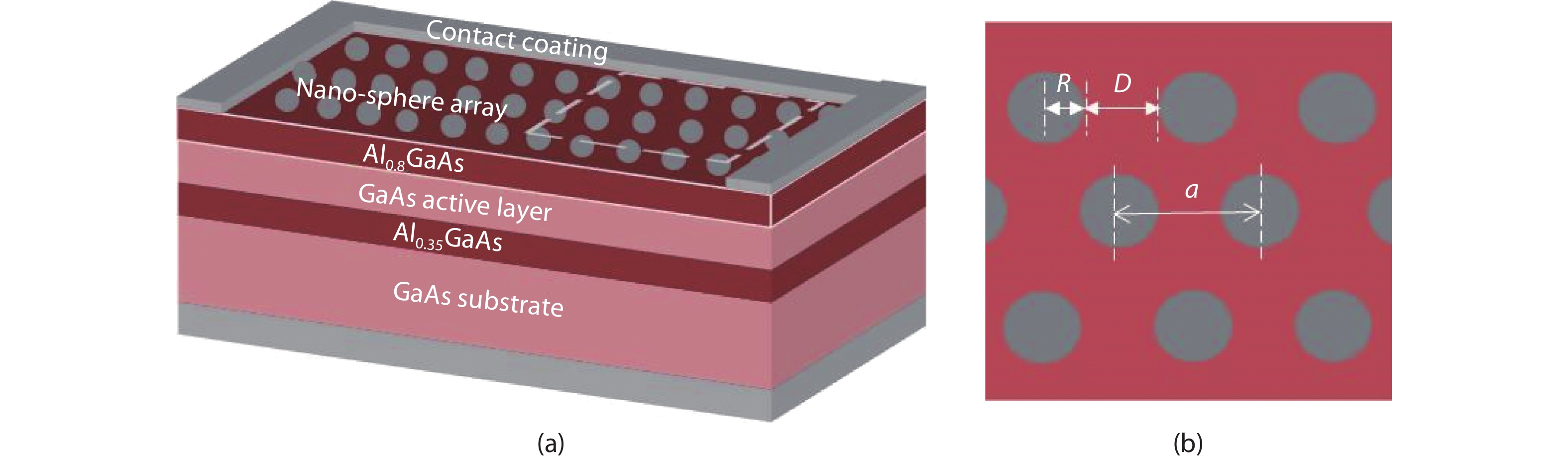
Fig. 1.
(Color online) (a) Schematic of the GaAs solar cell with nano-sphere array in side view. (b) Schematic top view of the nano-sphere surface array.
ARTICLES
Yinsheng Peng, Shufeng Gong, Kai Liu and Minghai Yao
Corresponding author: Minghai Yao, E-mail: ymh@zjut.edu.cn
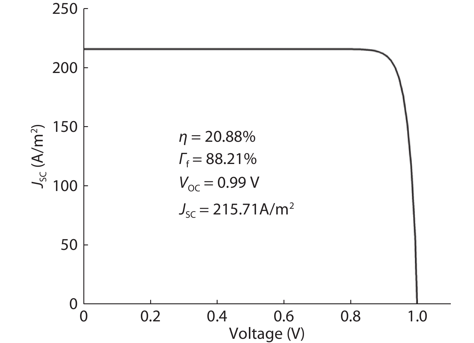
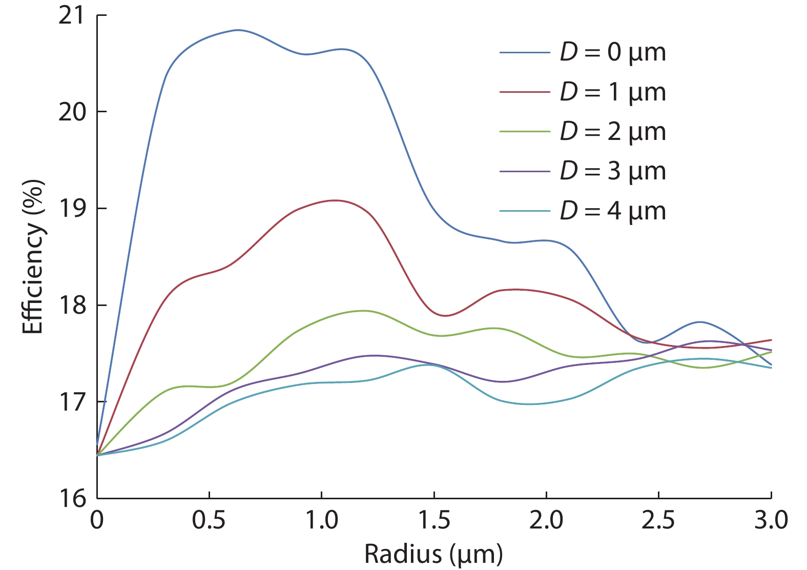
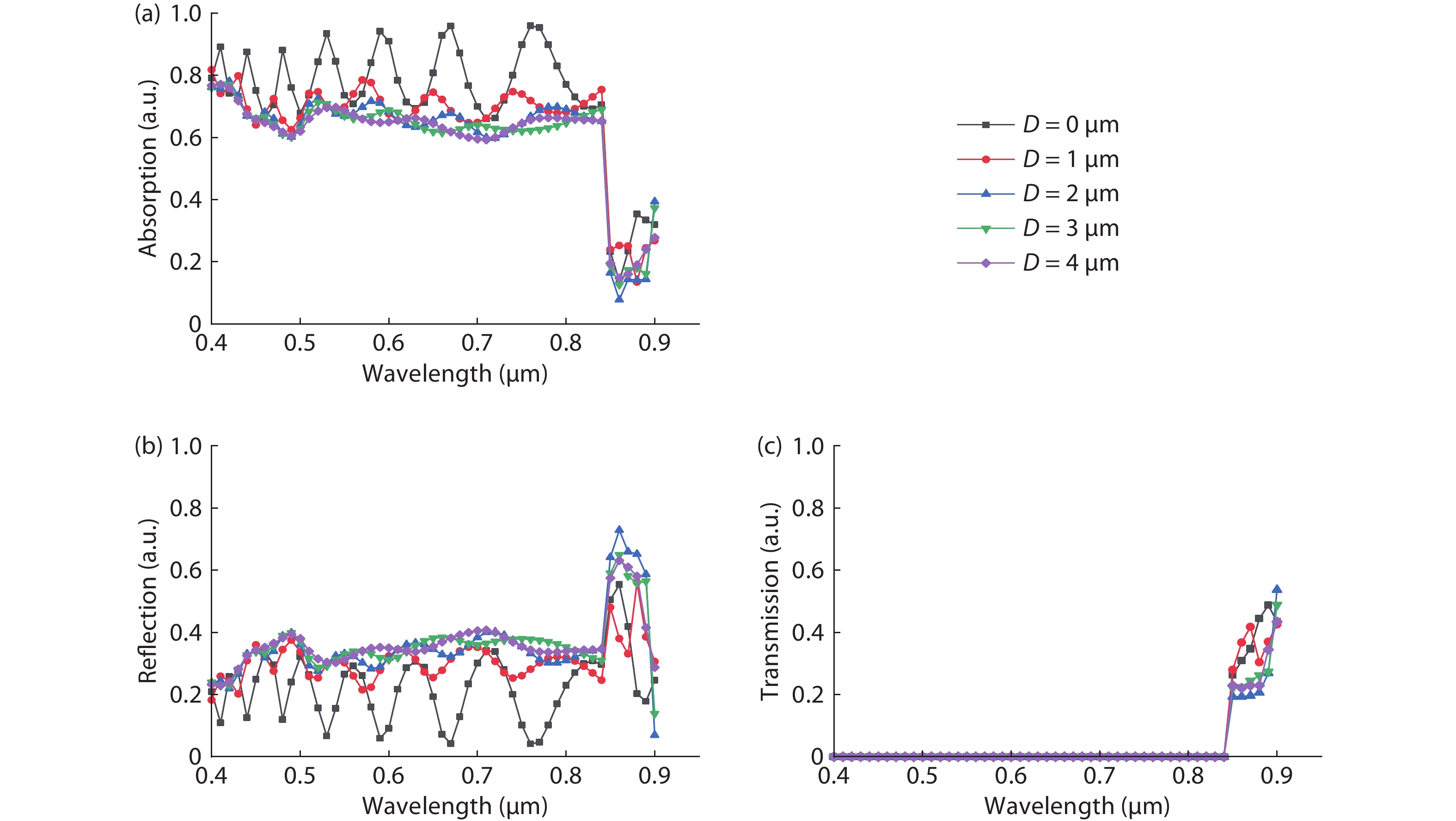
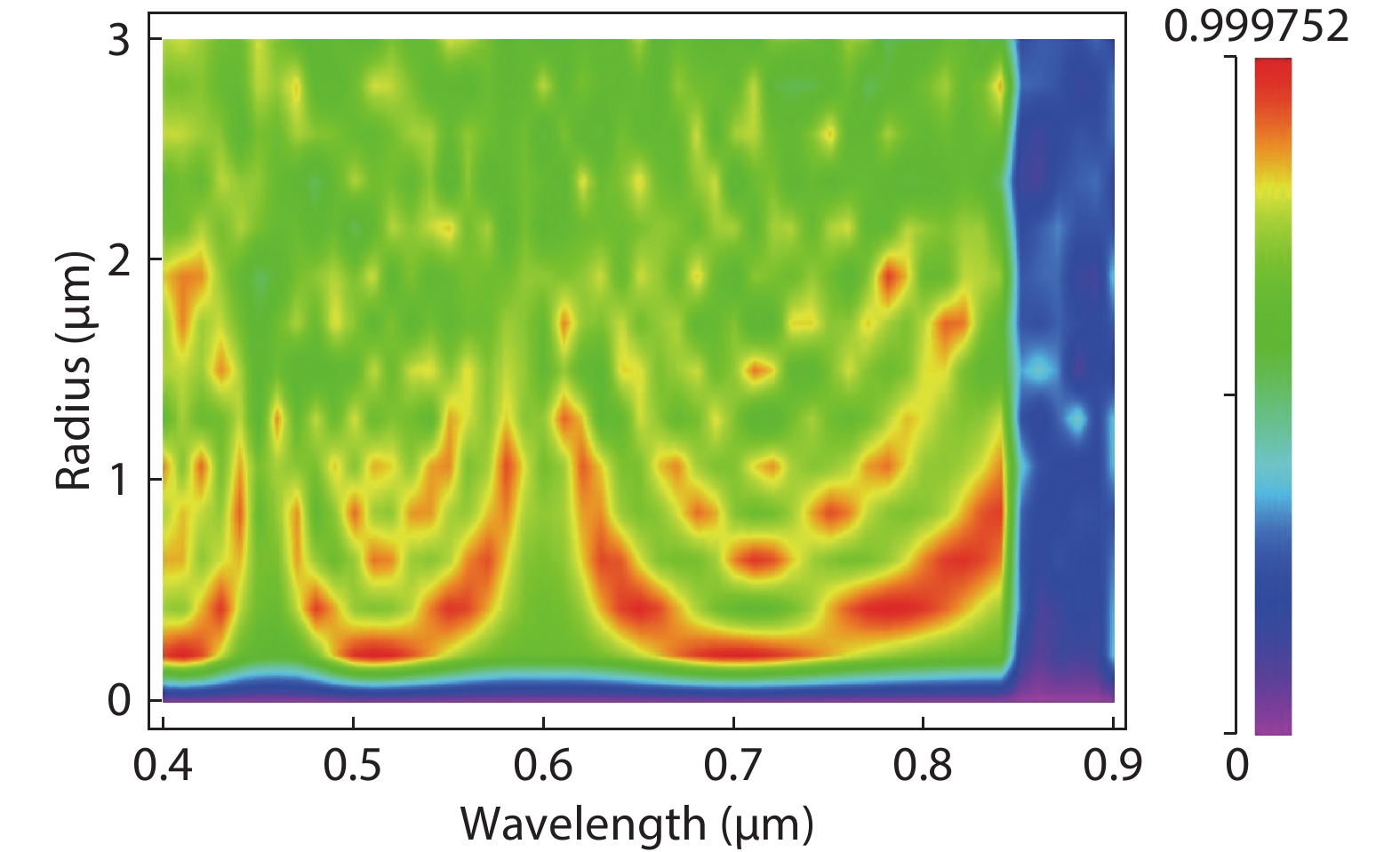
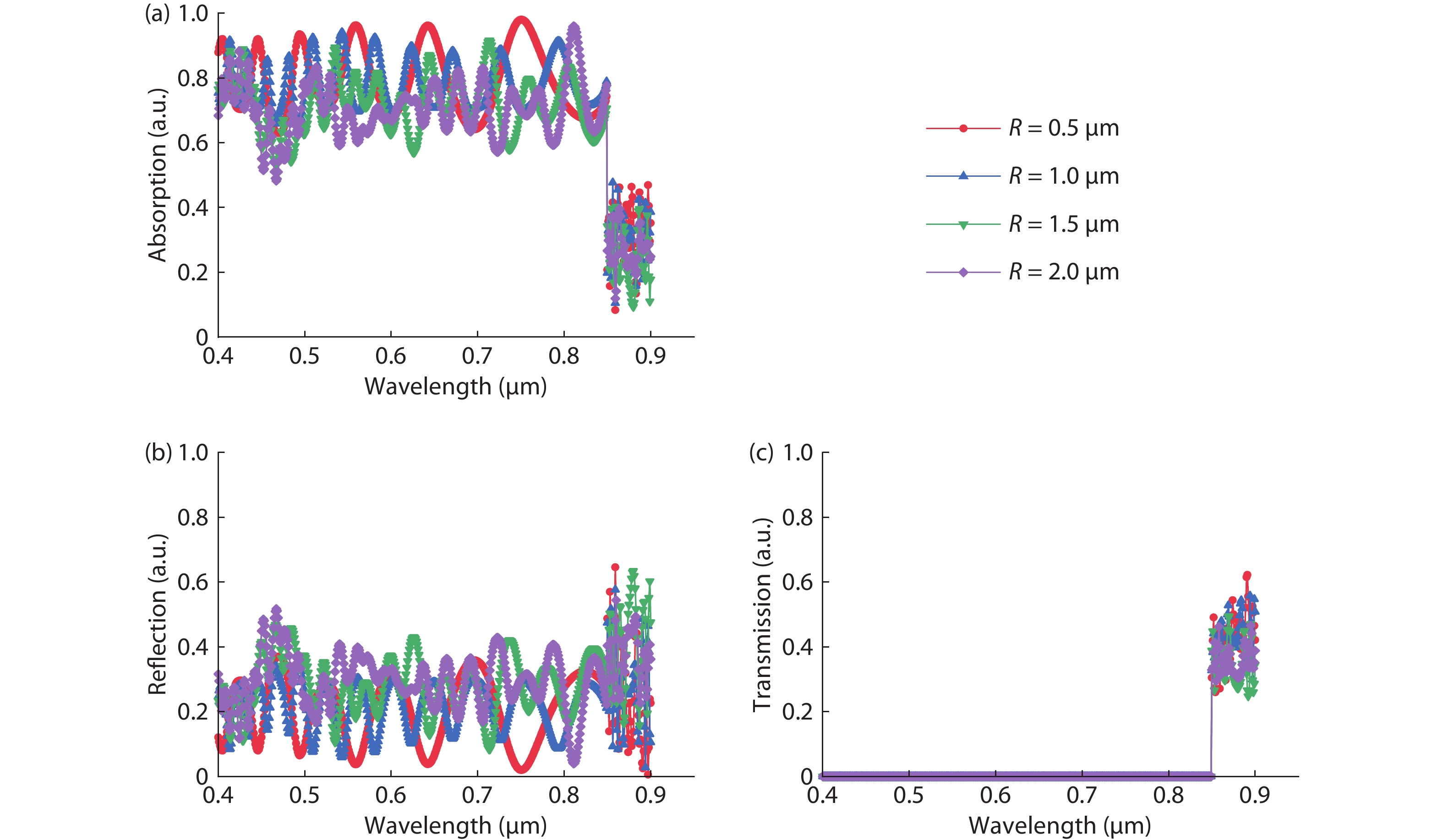
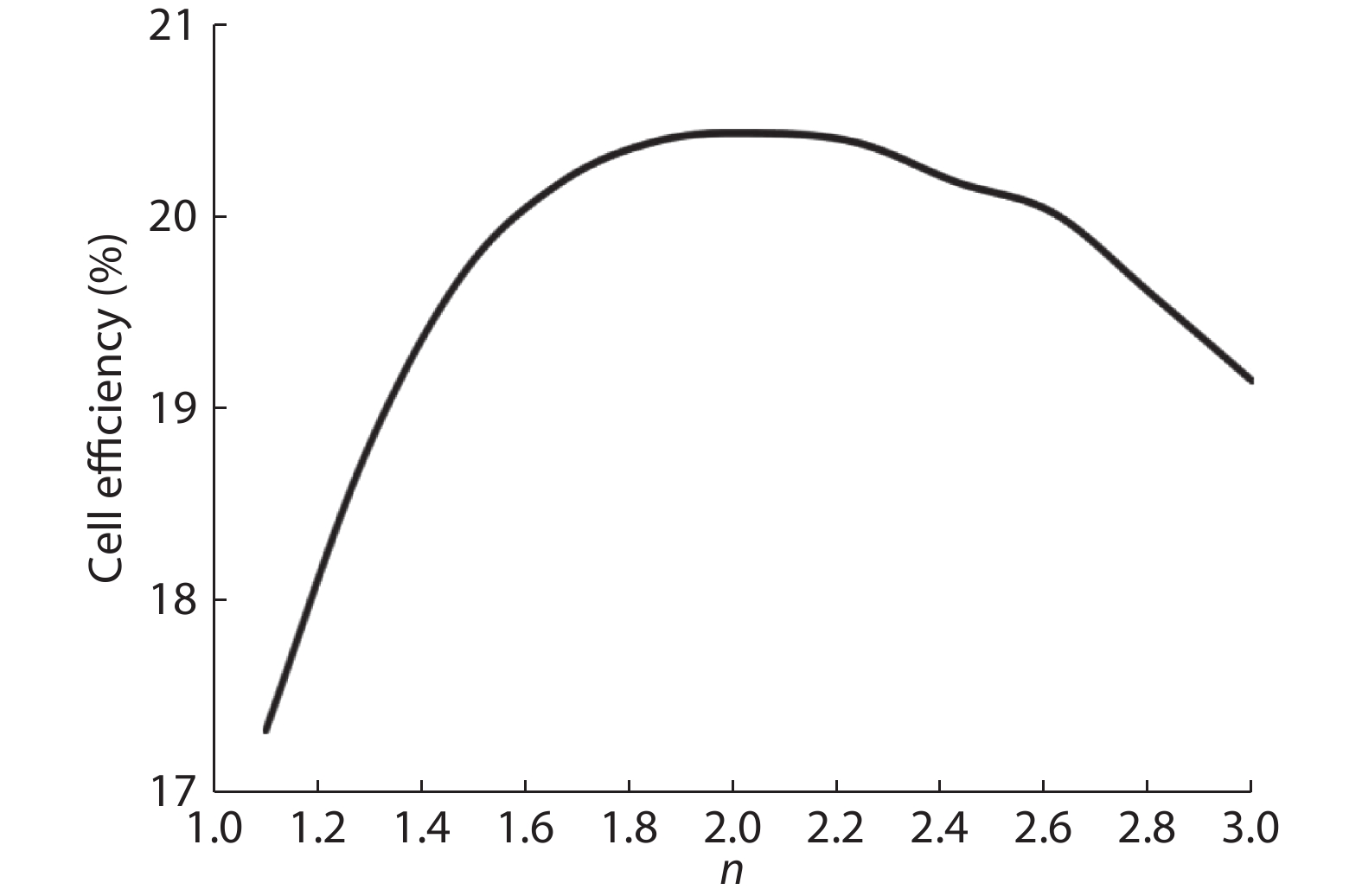
Abstract: In this paper, we present our efforts on simulating and analyzing the effect of two-dimensional nano-sphere surface array on the characteristic of GaAs solar cells. Based on the scattering and diffraction theory of the photonic crystals, the simulation results show that the distance of adjacent nano-spheres (D) has the pronounced influence on the conversion efficiency and exhibits much poor tolerance, the absolutely conversion efficiency is reduced by exceeding of 2% as the D varies from 0 to 1 μm, in addition, the lower conversion efficiency (< 18%) is exhibited and almost remains unaltered when the D is of > 2 μm. The radius (R) of nano-spheres demonstrates much great tolerance. For D = 0, the solar cells exhibit high conversion efficiency (> 20%) and the efficiency is only varied by less than 1% when R is varied in a very wide region of 0.3–1.2 μm. One can also find out that there is good tolerance for efficiency around the optimal value of refractive index and there is only about 0.2% decrease in final cell efficiency for around ±24% variation in the optimal values, which implys that it does not demand high precision processing equipment and the whole nano-sphere array could be fully complemented using self-assembled chemical methods.
Keywords: GaAs solar cell, nano-sphere array, reflection, absorption, conversion efficiency
| [1] |
Kitatani T, Yazawa Y, Watahiki S, et al. Optimal growth procedure of GaInP/GaAs heterostructure for high-efficiency solar cells. Sol Energy Mater Sol Cells, 1998, 50, 221 doi: 10.1016/S0927-0248(97)00151-7
|
| [2] |
Takamoto T, Yamaguchi M, Taylor S, J et al. Radiation resistance of high-efficiency InGaP/GaAs tandem solar cells. Sol Energy Mater Sol Cells, 1999, 58, 265 doi: 10.1016/S0927-0248(99)00003-3
|
| [3] |
Garcia I, Rey-Stolle B, Galiana C, et al. A 32.6% efficient lattice-matched dual-junction solar cell working at 1000 suns. Appl Phys Lett, 2009, 94, 053509 doi: 10.1063/1.3078817
|
| [4] |
Zhao J H, Wang A H, Green M A, et al. 19.8% efficient " honeycomb” textured multicrystalline and 24.4% monocrystalline silicon solar cells. Appl Phys Lett, 1998, 73, 1991 doi: 10.1063/1.122345
|
| [5] |
Tao M, Zhou W D, Yang H J, et al. Surface texturing by solution deposition for omnidirectional antireflection. Appl Phys Lett, 2007, 91, 081118 doi: 10.1063/1.2775805
|
| [6] |
Yerokhov V Y, Hezel R, Lipinski M, et al. Cost-effective methods of texturing for silicon solar cells. Sol Energy Mater Sol Cells, 2002, 72, 291 doi: 10.1016/S0927-0248(01)00177-5
|
| [7] |
Dewan R, Marinkovic M, Noriega R, et al. Light trapping in thin-film silicon solar cells with submicron surface texture. Opt Express, 2009, 17, 23058 doi: 10.1364/OE.17.023058
|
| [8] |
Zhao J, Wang A, Altermatt P, et al. Twenty-four percent efficient silicon solar cells with double layer antireflection coatings and reduced resistance loss. Appl Phys Lett, 1995, 66, 3636 doi: 10.1063/1.114124
|
| [9] |
Green M A. Two new efficient crystalline silicon light-trapping textures. Prog Photovolt Res Appl, 1999, 7, 317 doi: 10.1002/(SICI)1099-159X(199907/08)7:4<317::AID-PIP282>3.0.CO;2-3
|
| [10] |
Lam N D, Kim Y, Kim K, et al. Improved optical absorption and photocurrent of GaAs solar cells with hexagonal micro-hole array surface texturing. J Cryst Growth, 2013, 370, 244 doi: 10.1016/j.jcrysgro.2012.08.008
|
| [11] |
Chattopadhyay S, Huang Y F, Jen Y J, et al. Anti-reflecting and photonic nanostructures. Mater Sci Eng R, 2010, 69, 1 doi: 10.1016/j.mser.2010.04.001
|
| [12] |
Yan B, Owens J M, Jiang C, et al. High-efficiency amorphous silicon alloy based solar cells and modules. Proc MRS Symp, 2005, 862
|
| [13] |
Springer J, Poruba A, Müllerova L, et al. Absorption loss at nanorough silver back reflector of thin-film silicon solar cells. J Appl Phys, 2004, 95, 1427 doi: 10.1063/1.1633652
|
| [14] |
Yablonovitch E, Cody G D. Intensity enhancement in textured optical sheets for solar cells. IEEE Trans Electron Devices, 1982, 29, 300 doi: 10.1109/T-ED.1982.20700
|
| [15] |
Green M A. Lambertian light trapping in textured solar cells and light-emitting diodes: Analytical solutions. Prog Photovolt Res Appl, 2002, 10, 235 doi: 10.1002/pip.404
|
| [16] |
Campbell P, Green M A. Light trapping properties of pyramidally textured surfaces. J Appl Phys, 1987, 62, 243 doi: 10.1063/1.339189
|
| [17] |
Munday J N, Atwater H A. Large integrated absorption enhancement in plasmonic solar cells by combining metallic gratings and antireflection coatings. Nano Lett, 2011, 11, 2195 doi: 10.1021/nl101875t
|
| [18] |
Krc J, Cernivec G, Campa A, et al. Optical and electrical modeling of Cu(In, Ga)Se2 solar cells. Opt Quantum Electron, 2006, 38, 1115 doi: 10.1007/s11082-006-9049-1
|
| [19] |
Zhou D, Biswas R. Photonic crystal enhanced light-trapping in thin film solar cells. J Appl Phys, 2008, 103, 093102 doi: 10.1063/1.2908212
|
| [20] |
Chang T H, Wu P H, Chen S H, et al. Efficiency enhancement in GaAs solar cells using self-assembled microspheres. Opt Express, 2009, 17, 6519 doi: 10.1364/OE.17.006519
|
| [21] |
Sun C, Jiang P, Jiang B. Broadband moth-eye antireflection coatings on silicon. Appl Phys Lett, 2008, 92, 061112 doi: 10.1063/1.2870080
|
| [22] |
Huang C K, Sun K W, Chang W. Efficiency enhancement of silicon solar cells using a nano-scale honeycomb broadband anti-reflection structure. Opt Express, 2012, 20, A85 doi: 10.1364/OE.20.000A85
|
| [23] |
Domınguez S, Garcıá O, Ezquer M, et al. Optimization of 1D photonic crystals to minimize the reflectance of silicon solar cells. Photonics Nanostruct: Fundam Appl, 2012, 10, 46 doi: 10.1016/j.photonics.2011.07.001
|
| [24] |
Tsai M, Tseng P, Chen H, et al. Enhanced conversion efficiency of a crystalline silicon solar cell with frustum nanorod arrays. Conference on Lasers and Electro-Optics: Laser Science to Photonic Applications, 2011
|
| [25] |
Yamada N, Kim O N, Tokimitsu T, et al. Optimization of anti-reflection moth-eye structures for use in crystalline silicon solar cells. Prog Photovolt Res Appl, 2011, 19, 134 doi: 10.1002/pip.994
|
| [26] |
Aspnes D E, Kelso S M, Logan R A, et al. Optical properties of Al xGa1− xAs. J Appl Phys, 1986, 60, 754 doi: 10.1063/1.337426
|
| [27] |
Rakic A D, Djurišic A B, Elazar J M, et al. Optical properties of metallic films for vertical-cavity optoelectronic devices. Appl Opt, 1998, 37, 5271 doi: 10.1364/AO.37.005271
|
| [28] |
Mir Y, Amine A, Bouabdellaoui M, et al. The window layers effect on the hardness improvement of space solar cells exposed to the 1 MeV electron irradiations. Opt Quantum Electron, 2013, 45, 1189 doi: 10.1007/s11082-013-9735-8
|
| [29] |
Gupta N D, Janyani V. Optical and electrical simulation studies of light trapping in GaAs thin film solar cells using 2D photonic-crystal. J Nanoelectron Optoelectron, 2016, 11, 368 doi: 10.1166/jno.2016.1912
|
| [30] |
Wang X, Khan M, Gray J L, et al. Design of GaAs solar cells operating close to the Shockley-Queisser limit. IEEE J Photovolt, 2013, 3, 737 doi: 10.1109/JPHOTOV.2013.2241594
|
| [31] |
Biswas R, Ding C G, Puscasu I, et al. Theory of subwavelength hole arrays coupled with photonic crystals for extraordinary thermal emission. Phys Rev B, 2006, 74, 045107 doi: 10.1103/PhysRevB.74.045107
|
| [32] |
Li Z Y, Lin L L. Photonic band structures solved by a plane-wave-based transfer-matrix method. Phys Rev E, 2003, 67, 046607 doi: 10.1103/PhysRevE.67.046607
|
| [33] |
ASTMG173-03, Standard Tables for Reference Solar Spectral Irradiances: Direct Normal and Hemispherical on 37 degree Tilted Surface. ASTM International, West Conshohocken, Pennsylvania, 2005
|
| [34] |
Gupta N, Janyani V. Design and optimization of photonic crystal diffraction grating based efficient light trapping structure for GaAs thin film solar cell. J Nanoelectron Optoelectron, 2016, 11, 407 doi: 10.1166/jno.2016.1914
|
| [35] |
Bermel P, Luo C, Zeng L et al. Improving thin-film crystalline silicon solar cell efficiencies with photonic crystals. Opt Exp, 2007, 15, 16986 doi: 10.1364/OE.15.016986
|
| [36] |
Gupta N P, Janyani V. Design and analysis of light trapping in thin film GaAs solar cells using 2-D photonic crystal structures at front surface. IEEE J Quantum Electron, 2017, 53, 1 doi: 10.1109/JQE.2017.2667638
|


Article views: 4956 Times PDF downloads: 63 Times Cited by: 0 Times
Received: 19 September 2019 Revised: 13 November 2019 Online: Accepted Manuscript: 22 November 2019Uncorrected proof: 27 November 2019Published: 02 January 2020
| Citation: |
Yinsheng Peng, Shufeng Gong, Kai Liu, Minghai Yao. Nano-sphere surface arrays based on GaAs solar cells[J]. Journal of Semiconductors, 2020, 41(1): 012701. doi: 10.1088/1674-4926/41/1/012701
****
Y S Peng, S F Gong, K Liu, M H Yao, Nano-sphere surface arrays based on GaAs solar cells[J]. J. Semicond., 2020, 41(1): 012701. doi: 10.1088/1674-4926/41/1/012701.

|
| [1] |
Kitatani T, Yazawa Y, Watahiki S, et al. Optimal growth procedure of GaInP/GaAs heterostructure for high-efficiency solar cells. Sol Energy Mater Sol Cells, 1998, 50, 221 doi: 10.1016/S0927-0248(97)00151-7
|
| [2] |
Takamoto T, Yamaguchi M, Taylor S, J et al. Radiation resistance of high-efficiency InGaP/GaAs tandem solar cells. Sol Energy Mater Sol Cells, 1999, 58, 265 doi: 10.1016/S0927-0248(99)00003-3
|
| [3] |
Garcia I, Rey-Stolle B, Galiana C, et al. A 32.6% efficient lattice-matched dual-junction solar cell working at 1000 suns. Appl Phys Lett, 2009, 94, 053509 doi: 10.1063/1.3078817
|
| [4] |
Zhao J H, Wang A H, Green M A, et al. 19.8% efficient " honeycomb” textured multicrystalline and 24.4% monocrystalline silicon solar cells. Appl Phys Lett, 1998, 73, 1991 doi: 10.1063/1.122345
|
| [5] |
Tao M, Zhou W D, Yang H J, et al. Surface texturing by solution deposition for omnidirectional antireflection. Appl Phys Lett, 2007, 91, 081118 doi: 10.1063/1.2775805
|
| [6] |
Yerokhov V Y, Hezel R, Lipinski M, et al. Cost-effective methods of texturing for silicon solar cells. Sol Energy Mater Sol Cells, 2002, 72, 291 doi: 10.1016/S0927-0248(01)00177-5
|
| [7] |
Dewan R, Marinkovic M, Noriega R, et al. Light trapping in thin-film silicon solar cells with submicron surface texture. Opt Express, 2009, 17, 23058 doi: 10.1364/OE.17.023058
|
| [8] |
Zhao J, Wang A, Altermatt P, et al. Twenty-four percent efficient silicon solar cells with double layer antireflection coatings and reduced resistance loss. Appl Phys Lett, 1995, 66, 3636 doi: 10.1063/1.114124
|
| [9] |
Green M A. Two new efficient crystalline silicon light-trapping textures. Prog Photovolt Res Appl, 1999, 7, 317 doi: 10.1002/(SICI)1099-159X(199907/08)7:4<317::AID-PIP282>3.0.CO;2-3
|
| [10] |
Lam N D, Kim Y, Kim K, et al. Improved optical absorption and photocurrent of GaAs solar cells with hexagonal micro-hole array surface texturing. J Cryst Growth, 2013, 370, 244 doi: 10.1016/j.jcrysgro.2012.08.008
|
| [11] |
Chattopadhyay S, Huang Y F, Jen Y J, et al. Anti-reflecting and photonic nanostructures. Mater Sci Eng R, 2010, 69, 1 doi: 10.1016/j.mser.2010.04.001
|
| [12] |
Yan B, Owens J M, Jiang C, et al. High-efficiency amorphous silicon alloy based solar cells and modules. Proc MRS Symp, 2005, 862
|
| [13] |
Springer J, Poruba A, Müllerova L, et al. Absorption loss at nanorough silver back reflector of thin-film silicon solar cells. J Appl Phys, 2004, 95, 1427 doi: 10.1063/1.1633652
|
| [14] |
Yablonovitch E, Cody G D. Intensity enhancement in textured optical sheets for solar cells. IEEE Trans Electron Devices, 1982, 29, 300 doi: 10.1109/T-ED.1982.20700
|
| [15] |
Green M A. Lambertian light trapping in textured solar cells and light-emitting diodes: Analytical solutions. Prog Photovolt Res Appl, 2002, 10, 235 doi: 10.1002/pip.404
|
| [16] |
Campbell P, Green M A. Light trapping properties of pyramidally textured surfaces. J Appl Phys, 1987, 62, 243 doi: 10.1063/1.339189
|
| [17] |
Munday J N, Atwater H A. Large integrated absorption enhancement in plasmonic solar cells by combining metallic gratings and antireflection coatings. Nano Lett, 2011, 11, 2195 doi: 10.1021/nl101875t
|
| [18] |
Krc J, Cernivec G, Campa A, et al. Optical and electrical modeling of Cu(In, Ga)Se2 solar cells. Opt Quantum Electron, 2006, 38, 1115 doi: 10.1007/s11082-006-9049-1
|
| [19] |
Zhou D, Biswas R. Photonic crystal enhanced light-trapping in thin film solar cells. J Appl Phys, 2008, 103, 093102 doi: 10.1063/1.2908212
|
| [20] |
Chang T H, Wu P H, Chen S H, et al. Efficiency enhancement in GaAs solar cells using self-assembled microspheres. Opt Express, 2009, 17, 6519 doi: 10.1364/OE.17.006519
|
| [21] |
Sun C, Jiang P, Jiang B. Broadband moth-eye antireflection coatings on silicon. Appl Phys Lett, 2008, 92, 061112 doi: 10.1063/1.2870080
|
| [22] |
Huang C K, Sun K W, Chang W. Efficiency enhancement of silicon solar cells using a nano-scale honeycomb broadband anti-reflection structure. Opt Express, 2012, 20, A85 doi: 10.1364/OE.20.000A85
|
| [23] |
Domınguez S, Garcıá O, Ezquer M, et al. Optimization of 1D photonic crystals to minimize the reflectance of silicon solar cells. Photonics Nanostruct: Fundam Appl, 2012, 10, 46 doi: 10.1016/j.photonics.2011.07.001
|
| [24] |
Tsai M, Tseng P, Chen H, et al. Enhanced conversion efficiency of a crystalline silicon solar cell with frustum nanorod arrays. Conference on Lasers and Electro-Optics: Laser Science to Photonic Applications, 2011
|
| [25] |
Yamada N, Kim O N, Tokimitsu T, et al. Optimization of anti-reflection moth-eye structures for use in crystalline silicon solar cells. Prog Photovolt Res Appl, 2011, 19, 134 doi: 10.1002/pip.994
|
| [26] |
Aspnes D E, Kelso S M, Logan R A, et al. Optical properties of Al xGa1− xAs. J Appl Phys, 1986, 60, 754 doi: 10.1063/1.337426
|
| [27] |
Rakic A D, Djurišic A B, Elazar J M, et al. Optical properties of metallic films for vertical-cavity optoelectronic devices. Appl Opt, 1998, 37, 5271 doi: 10.1364/AO.37.005271
|
| [28] |
Mir Y, Amine A, Bouabdellaoui M, et al. The window layers effect on the hardness improvement of space solar cells exposed to the 1 MeV electron irradiations. Opt Quantum Electron, 2013, 45, 1189 doi: 10.1007/s11082-013-9735-8
|
| [29] |
Gupta N D, Janyani V. Optical and electrical simulation studies of light trapping in GaAs thin film solar cells using 2D photonic-crystal. J Nanoelectron Optoelectron, 2016, 11, 368 doi: 10.1166/jno.2016.1912
|
| [30] |
Wang X, Khan M, Gray J L, et al. Design of GaAs solar cells operating close to the Shockley-Queisser limit. IEEE J Photovolt, 2013, 3, 737 doi: 10.1109/JPHOTOV.2013.2241594
|
| [31] |
Biswas R, Ding C G, Puscasu I, et al. Theory of subwavelength hole arrays coupled with photonic crystals for extraordinary thermal emission. Phys Rev B, 2006, 74, 045107 doi: 10.1103/PhysRevB.74.045107
|
| [32] |
Li Z Y, Lin L L. Photonic band structures solved by a plane-wave-based transfer-matrix method. Phys Rev E, 2003, 67, 046607 doi: 10.1103/PhysRevE.67.046607
|
| [33] |
ASTMG173-03, Standard Tables for Reference Solar Spectral Irradiances: Direct Normal and Hemispherical on 37 degree Tilted Surface. ASTM International, West Conshohocken, Pennsylvania, 2005
|
| [34] |
Gupta N, Janyani V. Design and optimization of photonic crystal diffraction grating based efficient light trapping structure for GaAs thin film solar cell. J Nanoelectron Optoelectron, 2016, 11, 407 doi: 10.1166/jno.2016.1914
|
| [35] |
Bermel P, Luo C, Zeng L et al. Improving thin-film crystalline silicon solar cell efficiencies with photonic crystals. Opt Exp, 2007, 15, 16986 doi: 10.1364/OE.15.016986
|
| [36] |
Gupta N P, Janyani V. Design and analysis of light trapping in thin film GaAs solar cells using 2-D photonic crystal structures at front surface. IEEE J Quantum Electron, 2017, 53, 1 doi: 10.1109/JQE.2017.2667638
|

 WeChat ID
Journal of Semiconductors © 2017 All Rights Reserved 京ICP备05085259号-2

 DownLoad: