


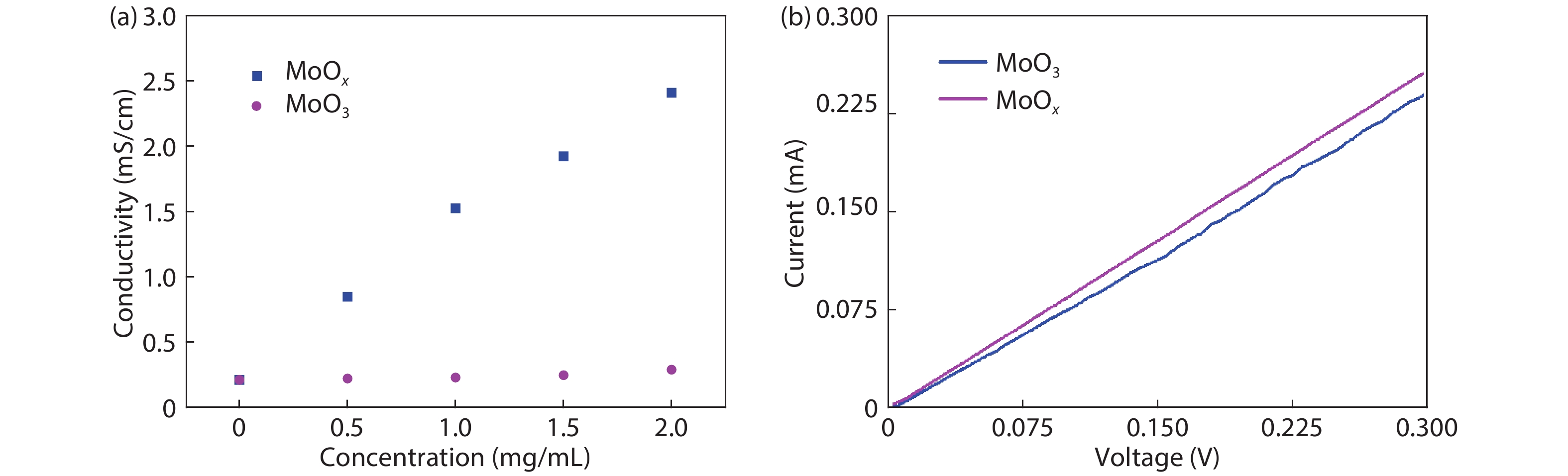
Fig. 1.
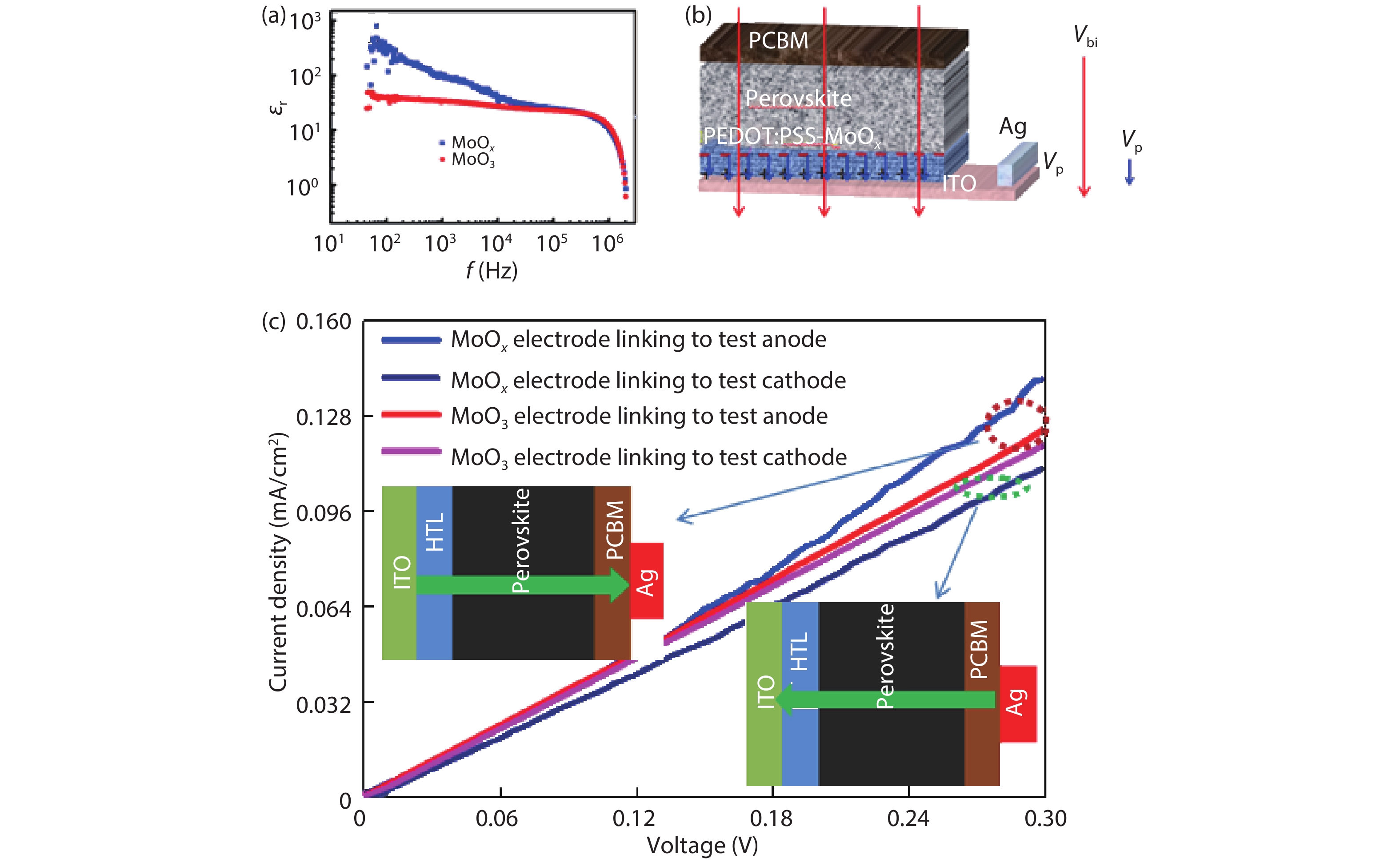
(Color online) (a) The in-plane conductivity of HTL films with 0–2 mg/mL MoOx or MoO3 incorporated into PEDOT:PSS. (b) I–V curves test for Ag/MoO3/ITO and Ag/MoOx/ITO.
ARTICLES
Yurong Jiang, Yue Yang, Yiting Liu, Shan Yan, Yanxing Feng and Congxin Xia
Corresponding author: Yurong Jiang, jiangyurong@whut.edu.cn; Congxin Xia, E-mail: xiacongxin@htu.edu.cn
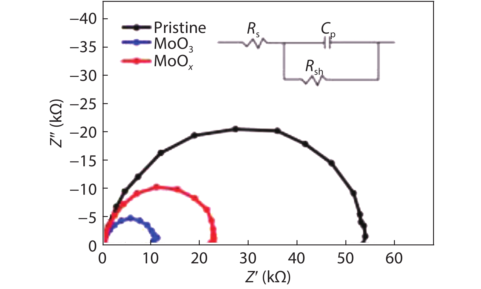
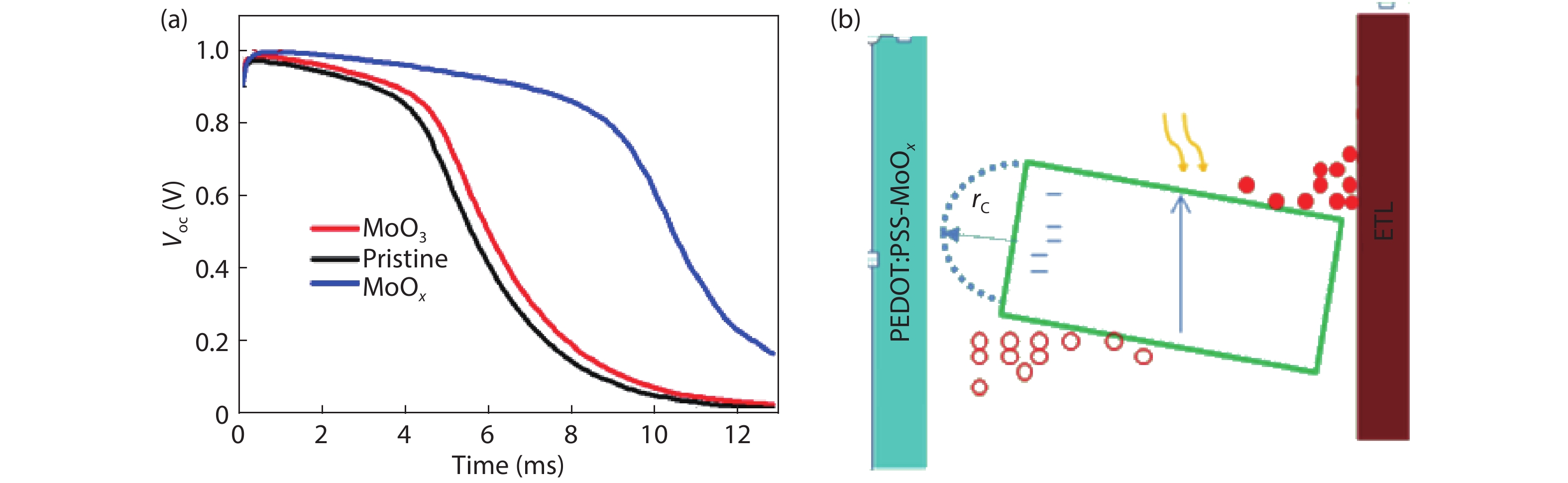
Abstract: In this paper, we investigate how interface-induced polarization affects the photovoltaic performance of hybrid perovskite solar cell (PSC) devices. The polarization of the hole transport layer (HTL) is regulated through incorporating metallic-like MoOx into PEDOT:PSS. The common MoO3 doped into PEDOT:PSS is used as a reference, and the device that used PEDOT:PSS-MoOx as the HTL shows an enhanced Jsc and FF compared to the reference device. The open-circuit photovoltage decay and impedance spectroscopy measurements indicate that trap-assisted recombination is effectively suppressed at the interface between the hybrid perovskite and the PEDOT:PSS-MoOx HTL, while severe trap assisted recombination takes place at the perovskite/PEDOT:PSS and perovskite/PEDOT:PSS-MoO3 interface. We attribute these experimental findings to the fact that the incorporation of metallic-like Mo5+ into PEDOT:PSS enhances the conductivity of HTL and the interface polarization between PEDTOT:PSS layer and perovskite, which helps to induce an interface polarization electric field to facilitate separation of charges and screen the recombination between the traps and free charges.
Key words: conductivity, hole-transporting layer, dielectric constant, polarization
| [1] |
De Wolf S, Holovsky J, Moon S J, et al. Organometallic halide perovskites: sharp optical absorption edge and its relation to photovoltaic performance. J Phys Chem Lett, 2014, 5(6), 1035 doi: 10.1021/jz500279b
|
| [2] |
Xing G, Mathews N, Sun S, et al. Long-range balanced electron-and hole-transport lengths in organic-inorganic CH3NH3PbI3. Science, 2013, 342(6156), 344 doi: 10.1126/science.1243167
|
| [3] |
Yoon H, Kang S M, Lee J K, et al. Hysteresis-free low-temperature-processed planar perovskite solar cells with 19.1% efficiency. Energy Environ Sci, 2016, 9(7), 2262 doi: 10.1039/C6EE01037G
|
| [4] |
Xing G, Mathews N, Lim S S, et al. Low-temperature solution-processed wavelength-tunable perovskites for lasing. Nat Mater, 2014, 13(5), 476 doi: 10.1038/nmat3911
|
| [5] |
Heo J H, Im S H, Noh J H, et al. Efficient inorganic–organic hybrid heterojunction solar cells containing perovskite compound and polymeric hole conductors. Nat Photonics, 2013, 7(6), 486 doi: 10.1038/nphoton.2013.80
|
| [6] |
Bryant D, Greenwood P, Troughton J, et al. A transparent conductive adhesive laminate electrode for high-efficiency organic-inorganic lead halide perovskite solar cells. Adv Mater, 2014, 26(44), 7499 doi: 10.1002/adma.201403939
|
| [7] |
Jiang Q, Zhang L, Wang H, et al. Enhanced electron extraction using SnO2 for high-efficiency planar-structure HC(NH2)2PbI3-based perovskite solar cells. Nat Energy, 2016, 2(1), 1 doi: 10.1038/nenergy.2016.177
|
| [8] |
Aeineh N, Barea E M, Behjat A, et al. Inorganic surface engineering to enhance perovskite solar cell efficiency. ACS Appl Mater Interfaces, 2017, 9(15), 13181 doi: 10.1021/acsami.7b01306
|
| [9] |
Gonzalez-Pedro V, Juarez-Perez E J, Arsyad W S, et al. General working principles of CH3NH3PbX3 perovskite solar cells. Nano Lett, 2014, 14(2), 888 doi: 10.1021/nl404252e
|
| [10] |
Yang K, Fu J, Hu L, et al. Impact of ZnO photoluminescence on organic photovoltaic performance. ACS Appl Mater Interfaces, 2018, 10(46), 39962 doi: 10.1021/acsami.8b14224
|
| [11] |
NREL chart. http://www.nrel.gov/ncpv/images/efficiency_chart. jpg. 2016
|
| [12] |
Xie J, Yu X, Sun X, et al. Improved performance and air stability of planar perovskite solar cells via interfacial engineering using a fullerene amine interlayer. Nano Energy, 2016, 28, 330 doi: 10.1016/j.nanoen.2016.08.048
|
| [13] |
Kim H, Lim K G, Lee T W. Planar heterojunction organometal halide perovskite solar cells: roles of interfacial layers. Energy Environ Sci, 2016, 9(1), 12 doi: 10.1039/C5EE02194D
|
| [14] |
Wang Z K, Gong X, Li M, et al. Induced crystallization of perovskites by a perylene underlayer for high-performance solar cells. ACS Nano, 2016, 10(5), 5479 doi: 10.1021/acsnano.6b01904
|
| [15] |
Liu X, Li B, Zhang N, et al. Multifunctional RbCl dopants for efficient inverted planar perovskite solar cell with ultra-high fill factor, negligible hysteresis and improved stability. Nano Energy, 2018, 53, 567 doi: 10.1016/j.nanoen.2018.09.023
|
| [16] |
Hu L, Li M, Yang K, et al. PEDOT:PSS monolayers to enhance the hole extraction and stability of perovskite solar cells. J Mater Chem A, 2018, 6(34), 16583 doi: 10.1039/C8TA05234D
|
| [17] |
Qian M, Li M, Shi X B, et al. Planar perovskite solar cells with 15.75% power conversion efficiency by cathode and anode interfacial modification. J Mater Chem A, 2015, 3(25), 13533 doi: 10.1039/C5TA02265G
|
| [18] |
Zhao L, Luo D, Wu J, et al. High-performance inverted planar heterojunction perovskite solar cells based on lead acetate precursor with efficiency exceeding 18%. Adv Funct Mater, 2016, 26(20), 3508 doi: 10.1002/adfm.201601175
|
| [19] |
Juarez-Perez E J, Wuβler M, Fabregat-Santiago F, et al. Role of the selective contacts in the performance of lead halide perovskite solar cells. J Phys Chem Lett, 2014, 5(4), 680 doi: 10.1021/jz500059v
|
| [20] |
Bergmann V W, Weber S A, Ramos F J, et al. Real-space observation of unbalanced charge distribution inside a perovskite-sensitized solar cell. Nat Commun, 2014, 5, 5001 doi: 10.1038/ncomms6001
|
| [21] |
Abrusci A, Stranks S D, Docampo P, et al. High-performance perovskite-polymer hybrid solar cells via electronic coupling with fullerene monolayers. Nano Lett, 2013, 13(7), 3124 doi: 10.1021/nl401044q
|
| [22] |
Tress W, Marinova N, Moehl T, et al. Understanding the rate-dependent J–V hysteresis, slow time component, and aging in CH3NH3PbI3 perovskite solar cells: the role of a compensated electric field. Energy Environ Sci, 2015, 8(3), 995 doi: 10.1039/C4EE03664F
|
| [23] |
Crispin X, Jakobsson F L, Crispin A, et al. The origin of the high conductivity of poly (3, 4-ethylenedioxythiophene)− poly (styrenesulfonate)(PEDOT−PSS) plastic electrodes. Chem Mater, 2006, 18(18), 4354 doi: 10.1021/cm061032+
|
| [24] |
Zheng X, Bai Y, Xiao S, et al. Strategies for improving efficiency and stability of perovskite solar cells. MRS Adv, 2017, 2, 3051 doi: 10.1557/adv.2017.485
|
| [25] |
Huang X, Wang K, Yi C, et al. Efficient perovskite hybrid solar cells by highly electrical conductive PEDOT:PSS hole transport layer. Adv Energy Mater, 2016, 6(3), 1501773 doi: 10.1002/aenm.201501773
|
| [26] |
Anusca I, Balčiūnas S, Gemeiner P, et al. Dielectric response: answer to many questions in the methylammonium lead halide solar cell absorbers. Adv Energy Mater, 2017, 7, 1700600 doi: 10.1002/aenm.201700600
|
| [27] |
Jiang Y, Li C, Liu H, et al. Poly (3, 4-ethylenedioxythiophene): poly (styrenesulfonate)(PEDOT: PSS)–molybdenum oxide composite films as hole conductors for efficient planar perovskite solar cells. J Mater Chem A, 2016, 4(25), 9958 doi: 10.1039/C6TA03658A
|
| [28] |
Wang Z, Lou Y, Naka S, et al. Direct comparison of solution- and vacuum-processed small molecular organic light-emitting devices with a mixed single layer. ACS Appl Mater Interfaces, 2011, 3(7), 2496 doi: 10.1021/am2003729
|
| [29] |
Schulz P, Tiepelt J O, Christians J A, et al. High-work-function molybdenum oxide hole extraction contacts in hybrid organic–inorganic perovskite solar cells. ACS Appl Mater Interfaces, 2016, 8(46), 31491 doi: 10.1021/acsami.6b10898
|
| [30] |
Kim H S, Cook J B, Lin H, et al. Oxygen vacancies enhance pseudocapacitive charge storage properties of MoO3− x. Nat Mater, 2017, 16(4), 454 doi: 10.1038/nmat4810
|
| [31] |
Lee M H, Chen L, Li N, et al. MoO3-induced oxidation doping of PEDOT: PSS for high performance full-solution-processed inverted quantum-dot light emitting diodes. J Mater Chem C, 2017, 5(40), 10555 doi: 10.1039/C7TC03700G
|
| [32] |
Nguyen W H, Bailie C D, Unger E L, et al. Enhancing the hole-conductivity of spiro-OMeTAD without oxygen or lithium salts by using spiro (TFSI)2 in perovskite and dye-sensitized solar cells. J Am Chem Soc, 2014, 136(31), 10996 doi: 10.1021/ja504539w
|
| [33] |
Wang N, Zhao K, Ding T, et al. Improving interfacial charge recombination in planar heterojunction perovskite photovoltaics with small molecule as electron transport layer. Adv Energy Mater, 2017, 7(18), 1700522 doi: 10.1002/aenm.201700522
|
| [34] |
Li Z, Tinkham J, Schulz P, et al. Acid additives enhancing the conductivity of Spiro-OMeTAD toward high-efficiency and hysteresis-less planar perovskite solar cells. Adv Energy Mater, 2017, 7(4), 1601451 doi: 10.1002/aenm.201601451
|
| [35] |
Shao Y, Yuan Y, Huang J. Correlation of energy disorder and open-circuit voltage in hybrid perovskite solar cells. Nat Energy, 2016, 1(1), 1 doi: 10.1038/nenergy.2015.1
|
| [36] |
Dualeh A, Moehl T, Tétreault N, et al. Impedance spectroscopic analysis of lead iodide perovskite-sensitized solid-state solar cells. ACS Nano, 2014, 8(1), 362 doi: 10.1021/nn404323g
|
| [37] |
Pockett A, Eperon G E, Peltola T, et al. Characterization of planar lead halide perovskite solar cells by impedance spectroscopy, open-circuit photovoltage decay, and intensity-modulated photovoltage/photocurrent spectroscopy. J Phys Chem C, 2015, 119(7), 3456 doi: 10.1021/jp510837q
|
| [38] |
Humada A M, Hojabri M, Mekhilef S, et al. Solar cell parameters extraction based on single and double-diode models: A review. Renew Sustain Energy Rev, 2016, 56, 494 doi: 10.1016/j.rser.2015.11.051
|
| [39] |
Tan F, Qu S, Jiang Q, et al. Interpenetrated inorganic hybrids for efficiency enhancement of PbS quantum dot solar cells. Adv Energy Mater, 2014, 4, 1400512 doi: 10.1002/aenm.201400512
|
| [40] |
Liu Z, Niu S, Wang N. Light illumination intensity dependence of photovoltaic parameter in polymer solar cells with ammonium heptamolybdate as hole extraction layer. J Colloid Interface Sci, 2018, 509, 171 doi: 10.1016/j.jcis.2017.09.010
|
| [41] |
Baumann A, Tvingstedt K, Heiber M C, et al. Persistent photovoltage in methylammonium lead iodide perovskite solar cells. Appl Mater, 2014, 2(8), 081501 doi: 10.1063/1.4885255
|
| [42] |
Tan F, Tan H, Saidaminov M I, et al. In situ back-contact passivation improves photovoltage and fill factor in perovskite solar cells. Adv Mater, 2019, 31(14), 1807435 doi: 10.1002/adma.201807435
|
| [43] |
Shao Y, Xiao Z, Bi C, et al. Origin and elimination of photocurrent hysteresis by fullerene passivation in CH3NH3PbI3 planar heterojunction solar cells. Nat Commun, 2014, 5, 5784 doi: 10.1038/ncomms6784
|
| [44] |
Hu L, Sun K, Wang M, et al. Inverted planar perovskite solar cells with a high fill factor and negligible hysteresis by the dual effect of NaCl-doped PEDOT: PSS. ACS Appl Mater Interfaces, 2017, 9(50), 43902 doi: 10.1021/acsami.7b14592
|
| [45] |
Kuik M, Koster L J, Wetzelaer G A, et al. Trap-assisted recombination in disordered organic semiconductors. Phys Rev Lett, 2011, 107(25), 256805 doi: 10.1103/PhysRevLett.107.256805
|
| [46] |
Sapori D, Kepenekian M, Pedesseau L, et al. Quantum confinement and dielectric profiles of colloidal nanoplatelets of halide inorganic and hybrid organic–inorganic perovskites. Nanoscale, 2016, 8(12), 6369 doi: 10.1039/C5NR07175E
|
| [47] |
Brenner T M, Egger D A, Kronik L, et al. Hybrid organic–inorganic perovskites: low-cost semiconductors with intriguing charge-transport properties. Nat Rev Mater, 2016, 1(1), 1 doi: 10.1038/natrevmats.2015.7
|


Article views: 5059 Times PDF downloads: 77 Times Cited by: 0 Times
Received: 01 March 2020 Revised: 23 March 2020 Online: Accepted Manuscript: 21 April 2020Uncorrected proof: 22 April 2020Published: 13 May 2020
| Citation: |
Yurong Jiang, Yue Yang, Yiting Liu, Shan Yan, Yanxing Feng, Congxin Xia. Mo5+ doping induced interface polarization for improving performance of planar perovskite solar cells[J]. Journal of Semiconductors, 2020, 41(5): 052203. doi: 10.1088/1674-4926/41/5/052203
****
Y R Jiang, Y Yang, Y T Liu, S Yan, Y X Feng, C X Xia, Mo5+ doping induced interface polarization for improving performance of planar perovskite solar cells[J]. J. Semicond., 2020, 41(5): 052203. doi: 10.1088/1674-4926/41/5/052203.

|
| [1] |
De Wolf S, Holovsky J, Moon S J, et al. Organometallic halide perovskites: sharp optical absorption edge and its relation to photovoltaic performance. J Phys Chem Lett, 2014, 5(6), 1035 doi: 10.1021/jz500279b
|
| [2] |
Xing G, Mathews N, Sun S, et al. Long-range balanced electron-and hole-transport lengths in organic-inorganic CH3NH3PbI3. Science, 2013, 342(6156), 344 doi: 10.1126/science.1243167
|
| [3] |
Yoon H, Kang S M, Lee J K, et al. Hysteresis-free low-temperature-processed planar perovskite solar cells with 19.1% efficiency. Energy Environ Sci, 2016, 9(7), 2262 doi: 10.1039/C6EE01037G
|
| [4] |
Xing G, Mathews N, Lim S S, et al. Low-temperature solution-processed wavelength-tunable perovskites for lasing. Nat Mater, 2014, 13(5), 476 doi: 10.1038/nmat3911
|
| [5] |
Heo J H, Im S H, Noh J H, et al. Efficient inorganic–organic hybrid heterojunction solar cells containing perovskite compound and polymeric hole conductors. Nat Photonics, 2013, 7(6), 486 doi: 10.1038/nphoton.2013.80
|
| [6] |
Bryant D, Greenwood P, Troughton J, et al. A transparent conductive adhesive laminate electrode for high-efficiency organic-inorganic lead halide perovskite solar cells. Adv Mater, 2014, 26(44), 7499 doi: 10.1002/adma.201403939
|
| [7] |
Jiang Q, Zhang L, Wang H, et al. Enhanced electron extraction using SnO2 for high-efficiency planar-structure HC(NH2)2PbI3-based perovskite solar cells. Nat Energy, 2016, 2(1), 1 doi: 10.1038/nenergy.2016.177
|
| [8] |
Aeineh N, Barea E M, Behjat A, et al. Inorganic surface engineering to enhance perovskite solar cell efficiency. ACS Appl Mater Interfaces, 2017, 9(15), 13181 doi: 10.1021/acsami.7b01306
|
| [9] |
Gonzalez-Pedro V, Juarez-Perez E J, Arsyad W S, et al. General working principles of CH3NH3PbX3 perovskite solar cells. Nano Lett, 2014, 14(2), 888 doi: 10.1021/nl404252e
|
| [10] |
Yang K, Fu J, Hu L, et al. Impact of ZnO photoluminescence on organic photovoltaic performance. ACS Appl Mater Interfaces, 2018, 10(46), 39962 doi: 10.1021/acsami.8b14224
|
| [11] |
NREL chart. http://www.nrel.gov/ncpv/images/efficiency_chart. jpg. 2016
|
| [12] |
Xie J, Yu X, Sun X, et al. Improved performance and air stability of planar perovskite solar cells via interfacial engineering using a fullerene amine interlayer. Nano Energy, 2016, 28, 330 doi: 10.1016/j.nanoen.2016.08.048
|
| [13] |
Kim H, Lim K G, Lee T W. Planar heterojunction organometal halide perovskite solar cells: roles of interfacial layers. Energy Environ Sci, 2016, 9(1), 12 doi: 10.1039/C5EE02194D
|
| [14] |
Wang Z K, Gong X, Li M, et al. Induced crystallization of perovskites by a perylene underlayer for high-performance solar cells. ACS Nano, 2016, 10(5), 5479 doi: 10.1021/acsnano.6b01904
|
| [15] |
Liu X, Li B, Zhang N, et al. Multifunctional RbCl dopants for efficient inverted planar perovskite solar cell with ultra-high fill factor, negligible hysteresis and improved stability. Nano Energy, 2018, 53, 567 doi: 10.1016/j.nanoen.2018.09.023
|
| [16] |
Hu L, Li M, Yang K, et al. PEDOT:PSS monolayers to enhance the hole extraction and stability of perovskite solar cells. J Mater Chem A, 2018, 6(34), 16583 doi: 10.1039/C8TA05234D
|
| [17] |
Qian M, Li M, Shi X B, et al. Planar perovskite solar cells with 15.75% power conversion efficiency by cathode and anode interfacial modification. J Mater Chem A, 2015, 3(25), 13533 doi: 10.1039/C5TA02265G
|
| [18] |
Zhao L, Luo D, Wu J, et al. High-performance inverted planar heterojunction perovskite solar cells based on lead acetate precursor with efficiency exceeding 18%. Adv Funct Mater, 2016, 26(20), 3508 doi: 10.1002/adfm.201601175
|
| [19] |
Juarez-Perez E J, Wuβler M, Fabregat-Santiago F, et al. Role of the selective contacts in the performance of lead halide perovskite solar cells. J Phys Chem Lett, 2014, 5(4), 680 doi: 10.1021/jz500059v
|
| [20] |
Bergmann V W, Weber S A, Ramos F J, et al. Real-space observation of unbalanced charge distribution inside a perovskite-sensitized solar cell. Nat Commun, 2014, 5, 5001 doi: 10.1038/ncomms6001
|
| [21] |
Abrusci A, Stranks S D, Docampo P, et al. High-performance perovskite-polymer hybrid solar cells via electronic coupling with fullerene monolayers. Nano Lett, 2013, 13(7), 3124 doi: 10.1021/nl401044q
|
| [22] |
Tress W, Marinova N, Moehl T, et al. Understanding the rate-dependent J–V hysteresis, slow time component, and aging in CH3NH3PbI3 perovskite solar cells: the role of a compensated electric field. Energy Environ Sci, 2015, 8(3), 995 doi: 10.1039/C4EE03664F
|
| [23] |
Crispin X, Jakobsson F L, Crispin A, et al. The origin of the high conductivity of poly (3, 4-ethylenedioxythiophene)− poly (styrenesulfonate)(PEDOT−PSS) plastic electrodes. Chem Mater, 2006, 18(18), 4354 doi: 10.1021/cm061032+
|
| [24] |
Zheng X, Bai Y, Xiao S, et al. Strategies for improving efficiency and stability of perovskite solar cells. MRS Adv, 2017, 2, 3051 doi: 10.1557/adv.2017.485
|
| [25] |
Huang X, Wang K, Yi C, et al. Efficient perovskite hybrid solar cells by highly electrical conductive PEDOT:PSS hole transport layer. Adv Energy Mater, 2016, 6(3), 1501773 doi: 10.1002/aenm.201501773
|
| [26] |
Anusca I, Balčiūnas S, Gemeiner P, et al. Dielectric response: answer to many questions in the methylammonium lead halide solar cell absorbers. Adv Energy Mater, 2017, 7, 1700600 doi: 10.1002/aenm.201700600
|
| [27] |
Jiang Y, Li C, Liu H, et al. Poly (3, 4-ethylenedioxythiophene): poly (styrenesulfonate)(PEDOT: PSS)–molybdenum oxide composite films as hole conductors for efficient planar perovskite solar cells. J Mater Chem A, 2016, 4(25), 9958 doi: 10.1039/C6TA03658A
|
| [28] |
Wang Z, Lou Y, Naka S, et al. Direct comparison of solution- and vacuum-processed small molecular organic light-emitting devices with a mixed single layer. ACS Appl Mater Interfaces, 2011, 3(7), 2496 doi: 10.1021/am2003729
|
| [29] |
Schulz P, Tiepelt J O, Christians J A, et al. High-work-function molybdenum oxide hole extraction contacts in hybrid organic–inorganic perovskite solar cells. ACS Appl Mater Interfaces, 2016, 8(46), 31491 doi: 10.1021/acsami.6b10898
|
| [30] |
Kim H S, Cook J B, Lin H, et al. Oxygen vacancies enhance pseudocapacitive charge storage properties of MoO3− x. Nat Mater, 2017, 16(4), 454 doi: 10.1038/nmat4810
|
| [31] |
Lee M H, Chen L, Li N, et al. MoO3-induced oxidation doping of PEDOT: PSS for high performance full-solution-processed inverted quantum-dot light emitting diodes. J Mater Chem C, 2017, 5(40), 10555 doi: 10.1039/C7TC03700G
|
| [32] |
Nguyen W H, Bailie C D, Unger E L, et al. Enhancing the hole-conductivity of spiro-OMeTAD without oxygen or lithium salts by using spiro (TFSI)2 in perovskite and dye-sensitized solar cells. J Am Chem Soc, 2014, 136(31), 10996 doi: 10.1021/ja504539w
|
| [33] |
Wang N, Zhao K, Ding T, et al. Improving interfacial charge recombination in planar heterojunction perovskite photovoltaics with small molecule as electron transport layer. Adv Energy Mater, 2017, 7(18), 1700522 doi: 10.1002/aenm.201700522
|
| [34] |
Li Z, Tinkham J, Schulz P, et al. Acid additives enhancing the conductivity of Spiro-OMeTAD toward high-efficiency and hysteresis-less planar perovskite solar cells. Adv Energy Mater, 2017, 7(4), 1601451 doi: 10.1002/aenm.201601451
|
| [35] |
Shao Y, Yuan Y, Huang J. Correlation of energy disorder and open-circuit voltage in hybrid perovskite solar cells. Nat Energy, 2016, 1(1), 1 doi: 10.1038/nenergy.2015.1
|
| [36] |
Dualeh A, Moehl T, Tétreault N, et al. Impedance spectroscopic analysis of lead iodide perovskite-sensitized solid-state solar cells. ACS Nano, 2014, 8(1), 362 doi: 10.1021/nn404323g
|
| [37] |
Pockett A, Eperon G E, Peltola T, et al. Characterization of planar lead halide perovskite solar cells by impedance spectroscopy, open-circuit photovoltage decay, and intensity-modulated photovoltage/photocurrent spectroscopy. J Phys Chem C, 2015, 119(7), 3456 doi: 10.1021/jp510837q
|
| [38] |
Humada A M, Hojabri M, Mekhilef S, et al. Solar cell parameters extraction based on single and double-diode models: A review. Renew Sustain Energy Rev, 2016, 56, 494 doi: 10.1016/j.rser.2015.11.051
|
| [39] |
Tan F, Qu S, Jiang Q, et al. Interpenetrated inorganic hybrids for efficiency enhancement of PbS quantum dot solar cells. Adv Energy Mater, 2014, 4, 1400512 doi: 10.1002/aenm.201400512
|
| [40] |
Liu Z, Niu S, Wang N. Light illumination intensity dependence of photovoltaic parameter in polymer solar cells with ammonium heptamolybdate as hole extraction layer. J Colloid Interface Sci, 2018, 509, 171 doi: 10.1016/j.jcis.2017.09.010
|
| [41] |
Baumann A, Tvingstedt K, Heiber M C, et al. Persistent photovoltage in methylammonium lead iodide perovskite solar cells. Appl Mater, 2014, 2(8), 081501 doi: 10.1063/1.4885255
|
| [42] |
Tan F, Tan H, Saidaminov M I, et al. In situ back-contact passivation improves photovoltage and fill factor in perovskite solar cells. Adv Mater, 2019, 31(14), 1807435 doi: 10.1002/adma.201807435
|
| [43] |
Shao Y, Xiao Z, Bi C, et al. Origin and elimination of photocurrent hysteresis by fullerene passivation in CH3NH3PbI3 planar heterojunction solar cells. Nat Commun, 2014, 5, 5784 doi: 10.1038/ncomms6784
|
| [44] |
Hu L, Sun K, Wang M, et al. Inverted planar perovskite solar cells with a high fill factor and negligible hysteresis by the dual effect of NaCl-doped PEDOT: PSS. ACS Appl Mater Interfaces, 2017, 9(50), 43902 doi: 10.1021/acsami.7b14592
|
| [45] |
Kuik M, Koster L J, Wetzelaer G A, et al. Trap-assisted recombination in disordered organic semiconductors. Phys Rev Lett, 2011, 107(25), 256805 doi: 10.1103/PhysRevLett.107.256805
|
| [46] |
Sapori D, Kepenekian M, Pedesseau L, et al. Quantum confinement and dielectric profiles of colloidal nanoplatelets of halide inorganic and hybrid organic–inorganic perovskites. Nanoscale, 2016, 8(12), 6369 doi: 10.1039/C5NR07175E
|
| [47] |
Brenner T M, Egger D A, Kronik L, et al. Hybrid organic–inorganic perovskites: low-cost semiconductors with intriguing charge-transport properties. Nat Rev Mater, 2016, 1(1), 1 doi: 10.1038/natrevmats.2015.7
|
 19120027supp.pdf
|

|

 WeChat ID
Journal of Semiconductors © 2017 All Rights Reserved 京ICP备05085259号-2

 DownLoad:

