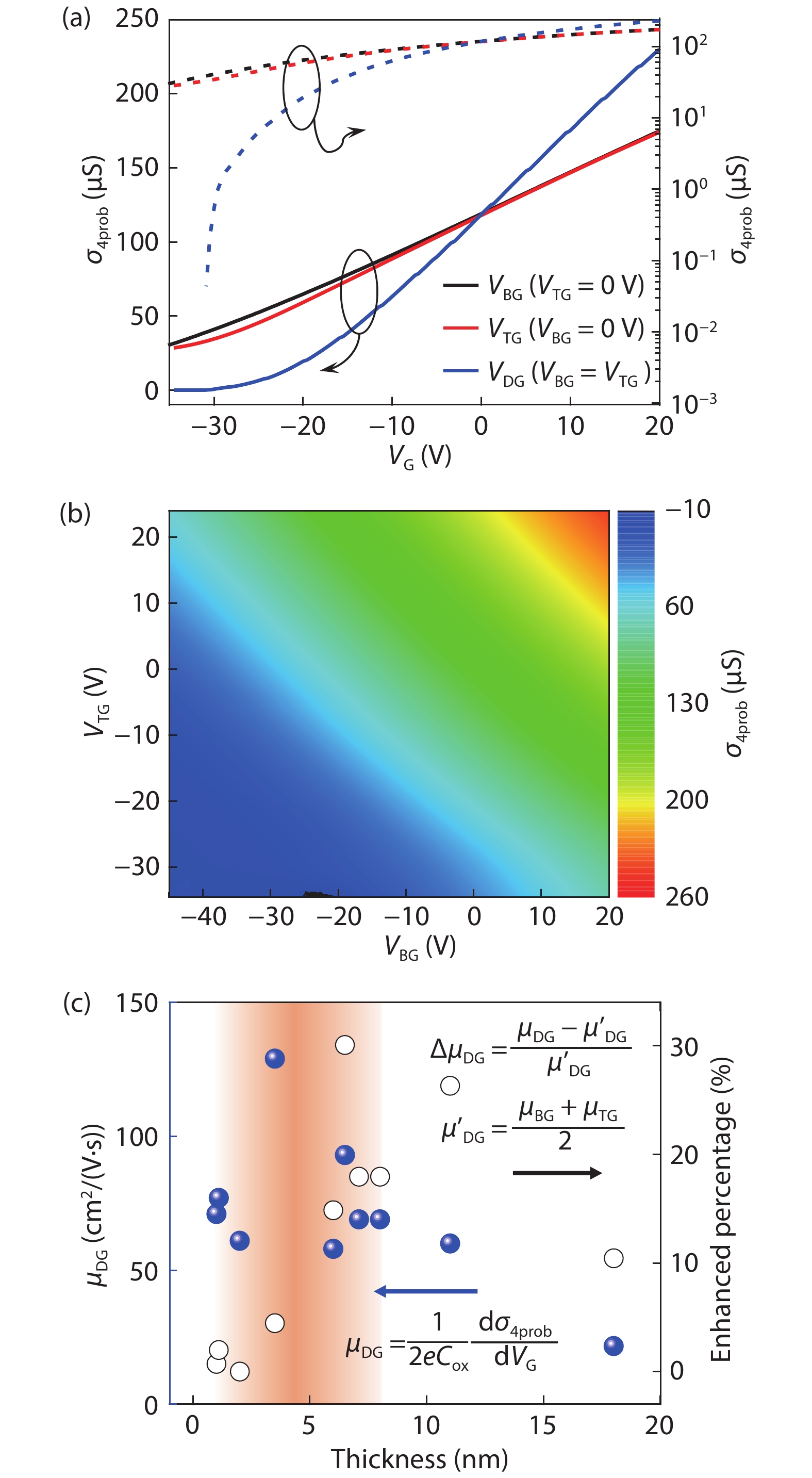
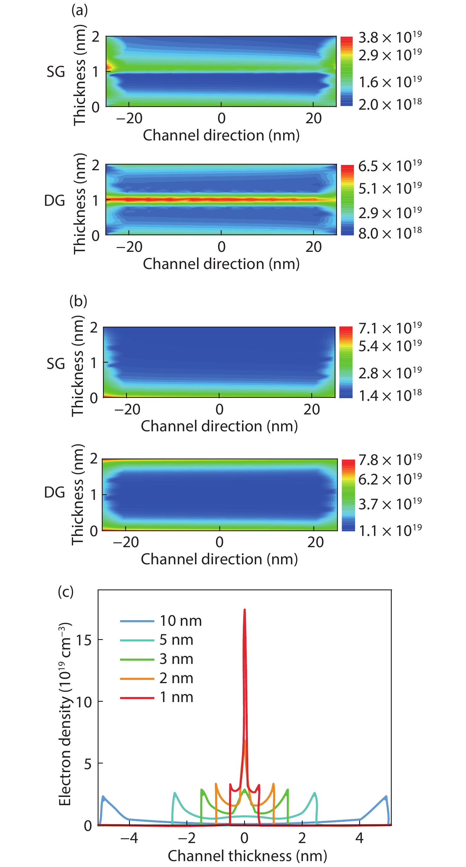
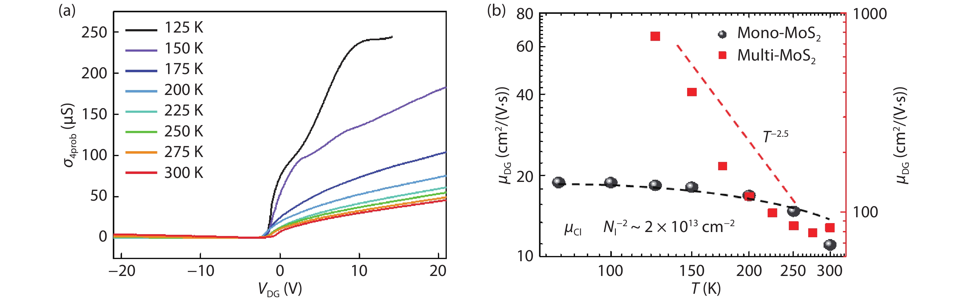
Processing math: 100%
J. Semicond. > 2020, Volume 41 > Issue 7 > 072904

ARTICLES

Charge transport and quantum confinement in MoS2 dual-gated transistors

Fuyou Liao1, 4, , Hongjuan Wang2, 3, , Xiaojiao Guo1, , Zhongxun Guo1, Ling Tong1, Antoine Riaud1, Yaochen Sheng1, Lin Chen1, Qingqing Sun1, Peng Zhou1, David Wei Zhang1, Yang Chai4, 5, Xiangwei Jiang3, Yan Liu2, and Wenzhong Bao1,

+ Author Affiliations

 Corresponding author: Yan Liu, Email: xdliuyan@xidian.edu.cn; Wenzhong Bao, baowz@fudan.edu.cn

DOI: 10.1088/1674-4926/41/7/072904

PDF

Turn off MathJax

Abstract: Semiconductive two dimensional (2D) materials have attracted significant research attention due to their rich band structures and promising potential for next-generation electrical devices. In this work, we investigate the MoS2 field-effect transistors (FETs) with a dual-gated (DG) architecture, which consists of symmetrical thickness for back gate (BG) and top gate (TG) dielectric. The thickness-dependent charge transport in our DG-MoS2 device is revealed by a four-terminal electrical measurement which excludes the contact influence, and the TCAD simulation is also applied to explain the experimental data. Our results indicate that the impact of quantum confinement effect plays an important role in the charge transport in the MoS2 channel, as it confines charge carriers in the center of the channel, which reduces the scattering and boosts the mobility compared to the single gating case. Furthermore, temperature-dependent transfer curves reveal that multi-layer MoS2 DG-FET is in the phonon-limited transport regime, while single layer MoS2 shows typical Coulomb impurity limited regime.

Key words: MoS2field effect transistorsdual-gatequantum confinementCoulomb impurity

Atomic thick two-dimensional (2D) layered materials, such as semi-metallic graphene and semiconductive transition metal dichalcogenides (TMDCs), have emerged as an attractive candidate for future electronic and optoelectrical materials[1-6]. Among them, molybdenum disulphide (MoS2) is a typical member of TMDCs and considered as a promising candidate for various device applications, mainly due to its prolific, thickness-dependent band structures[7-10]. The single-gated field-effect transistors (SG-FETs) based on MoS2 exhibit excellent carrier mobility (~ 200 cm2/(V·s)), high current on/off ratio (> 108), and low subthreshold swing approaching the fundamental thermal limit at room temperature[2]. The short channel effects (SCE) can also be suppressed due to the ultra-thin channel body[7, 11].

Since the bandgap size is dependent on the MoS2 layer number[12-14], bilayer (BL) or multilayer (ML) MoS2 tend to achieve higher mobility to carry larger driving current than that of monolayer MoS2. However, the BL or ML-MoS2 suffer from the degradation of SS and the current on/off ratio due to weaker channel electrostatic control. To overcome such a problem, the dual-gated (DG) structure, similar to that of Fin-FET technology, provides better electrostatic control over the channel region and is more achievable for 2D-TMDCs[15-18]. Liu et al. achieved a back-gate mobility of up to 517 cm2/(V·s) and an on/off ratio higher than 108 based on SiO2, Al2O3 as the back-gated and top-gated dielectric[19]. Our previously reported results based on a DG-FET with symmetrical back and top gates also indicate that the DG structure is able to modulate the threshold voltage (VTH) and SS by tuning back and top gates separately, and a superior channel current (ID) modulation can be achieved under the DG gating[20-22]. Nevertheless, the charge transport and current distribution influenced by DG structure have not been systematically discussed in TMDCs devices.

Here, we successfully fabricate the MoS2 DG-FETs with symmetric back gate (BG) and top gate (TG) based on monolayer and multilayer MoS2 films. The thickness-dependent charge transport in our MoS2 DG structure is revealed by a four-probe electrical measurement which excludes the contact influence, and TCAD simulation shows that the impact of quantum confinement effect exists in thin MoS2 sheet sandwiched by the DG. Such effect attenuates with larger thickness, but still exist in a 5-nm-thick channel. The temperature-dependent electrical measurement of our device also indicates that transport of multilayer MoS2 DG-FET is in the phonon-limited transport regime, while single layer MoS2 device shows typical Coulomb impurity (CI) limited regime.

The cross-sectional schematic of MoS2 DG-FET is depicted in Fig. 1(a). The fabrication process for such devices starts from the deposition of a 200-nm-thick Al2O3 layer by atom layer deposition (ALD, MNT-100-4) on a heavily doped Si substrate, which acts as a BG dielectric layer. Then multilayer MoS2 flakes are mechanically exfoliated on top of Al2O3, and a typical optical microscopic image is shown in Fig. 1(b). Uniform and rectangular shaped MoS2 sheets are selected for subsequent device fabrication. Raman characterization (laser excitation wavelength of 514 nm) is then carried out to confirm the layer number and crystalline quality, as shown in Fig. 1(c). To avoid lithography contamination, electrical contacts (5 nm Ti/30 nm Au) are patterned using a stencil mask technique[23]. Immediately after the contact deposition, another layer of 200-nm-thick Al2O3 is deposited by ALD as TG dielectric, followed by the formation of TG electrodes by traditional photo-lithography, metal evaporation, and lift-off. Electrical transport measurements are performed under an ambient condition with a semiconductor analyzer (Agilent, B1500a). Temperature-dependent measurement was carried out in a cryogenic vacuum probe-station.

Figure  1.  (Color online) (a) Side-view schematic illustration of a MoS2 DG-FET. (b) Optical microscopic image of an exfoliated MoS2 sheet on a 200-nm-thick Al2O3 substrate. (c) Raman spectra of MoS2 sheets with thickness ranging from 1L to 4L. (d) Optical image of a typical 4-terminal device, the top gate electrode is relatively thin (15 nm) but still conductive. The lower graph is a schematic of the 4-terminal device in which W is the channel width and L is the distance between two inner pads. V1 and V2 are used to gauge the voltage drop between two inner contacts.

The field-effect mobility μ is a crucial factor to characterize the FET performance. For most TMDCs-based FETs, the effective value of μ is mainly governed by the contact rather than the channel itself[24, 25]. In order to isolate the intrinsic mobility, we compensate for this effect by utilizing a four-terminal structure to exclude the contact effect. The upper graph of Fig. 1(d) is an optical image of our four-terminal device and the lower graph is a schematic diagram where the two inner voltage probes V1 and V2 are used to gauge the voltage drop. Then the four-terminal conductivity σ4prob=IDV1V2LW, where ID is the channel current and L and W are the length and width of the MoS2 channel inside the inner voltage probes, respectively.

The measured σ4prob as functions of BG, TG and DG modes are shown in Fig. 2(a). It is noted that results from BG and TG modes are highly coincident due to their symmetric gating capability, while a weak mismatch at negative gate voltage region can also be observed, which may result from their different dielectric-MoS2 interfaces. As for the BG, MoS2 is directly transferred on to the pre-deposited Al2O3, while for the TG, the interface quality degrades because of the absence of dangling bonds on MoS2 for deposition of Al2O3.

Figure  2.  (Color online) (a) Four-terminal conductivity σ4prob as functions of BG, TG and DG voltages. Solid and dashed curves correspond to linear and logarithmic coordinates, respectively. (b) 2D contour plot of σ4prob as functions of VBG and VTG at room temperature. (c) Mobility versus sheet thickness collected from 10 MoS2 DG-FETs work under DG mode.

It also shows that DG mode displays an improved channel electrostatic control than that of BG or TG. To further illustrate the gate modulation by BG and TG, a 2D contour plot of σ4prob as functions of VBG and VTG is then plotted in Fig. 2(b). Such 2D diagram shows parallel diagonal contours with constant current, and the slope of these contours line is approximately 1, indicating that the BG and TG exhibit the same capability to modulate the channel, since the oxidation layer capacitance of the back gate and top gate is nearly symmetrical (CBG /CTG ≈ 1).

For SG structure, the field-effect (FE) mobility can be estimated by μ=1eCoxdσdVG, where Cox is the gate capacitance per unit area (40 nF/cm2 for 200 nm of Al2O3), VG is the gate voltage, and e is the elementary charge. While in the case of a symmetric DG structure and considering top and bottom surfaces of MoS2 as parallel channels, we can estimate that the total conductivity σ’DG = σBG + σTG. Since C’ox-DG ≈ 2Cox, we expect that the quantity μ’DG = (μBG + μTG)/2 will be equal to μDG estimated by the σDGVDG curve. However, it appears that directly measured μDG is generally larger than μ’DG, which indicates the inadequacy of this parallel channel model. We then use ΔμDG = (μDGμ’DG)/μ’DG to quantify the mobility enhancement of dual gating, and plot in Fig. 2(c) ΔμDG and μDG as functions of the channel thickness. It is noted that both device mobility and ΔμDG reach a maximum with the MoS2 thickness in the range of 2–6 nm, and such thickness-dependent μDG deviates from previously reported results with only BG[24, 26, 27], indicating a different carrier transport mechanism in our DG-FETs.

Depending on the channel thickness, there is a competition of multiple mechanisms in our MoS2 DG-FETs: 1) larger current carrying ability in thicker channels, but with considerable interlayer resistance[24]; 2) current redistribution due to the DG induced quantum confinement effect; 3) electrical transport exposed to extrinsic Coulomb scattering from high-k dielectrics (e.g. Al2O3, HfO2) and interface for ultra-thin channels. Therefore, the experimental results exhibit their overall competitional effects. While the first and the third factors may have a negative effect on the mobility, we now focus on the quantum confinement effect, which may avoid the interfacial scattering and enhance the carrier mobility.

To ravel the impact from quantum confinement effect, the carrier density, and distribution of the DG-FETs are then simulated by using the van Dort model, the 1D Schrödinger equation, the density gradient model, and the modified local-density approximation (MLDA). The van Dort model computes the impact of electric field normal to the channel interface on the carrier density modification due to the quantization. Based on the energy band structures in the channel, the 1D Schrödinger equation was solved self-consistently with the Poisson equation. The eigenvalues and wave functions for electrons and holes were obtained with consideration of multi valleys in conduction and valence bands. The density gradient model added the quantum correction to the carrier distribution at interfaces in the device by introducing the reciprocal thermal energy, mass-driving term, and the smoothed potential[28]. In this model, the bandgap narrowing effect and apparent band-edge shifts caused by multistate configurations were involved. The MLDA model calculates the distribution of confined carriers near the dielectric/channel interface. In our simulation, the multi valley properties of conduction and valence bands were considered in MLDA model.

Figs. 3(a) and 3(b) compare the quantum-confinement impact on the simulated carrier redistribution in SG (VBG  = 10 V) and DG (VBG  = VTG  = 10 V) structures. In the DG structure, quantum confinement effect is rather prominent, it repulses carriers away from dielectric-MoS2 interfaces and confines carriers inside the channel, which can suppress phonon and Coulomb scattering at interfaces and contribute to the mobility improvement. On the opposite, the carriers in the SG structure are pushed towards one side of MoS2, amplifying the interface scattering. Fig. 3(c) shows the calculated carrier distribution in MoS2 DG device with a series of channel thicknesses, by considering quantum confinement effect. It is noticed that the impact of quantum confinement effect attenuates with larger thickness but still exist in a 5 nm thick channel.

Figure  3.  (Color online) (a) With and (b) without considering quantum confinement effect, the simulation results of carrier redistribution of a 2-nm-thick MoS2. The upper and lower panels show the simulation results from the SG (VBG = 10 V) and DG (VBG = VTG = 10 V) device, respectively. (c) The electron density in the channel of the DG MoS2 device versus channel thickness. The dielectric layer is 200 nm Al2O3. for all devices

Thus, a complete scenario for thickness dependence of MoS2 DG-FET can be: thicker MoS2 carries current larger but with less quantum confinement effect, and there are also trade-offs including large interlayer resistance and screening effect than weakens the gate control. For practical applications of MoS2 FETs, considering critical parameters including μ, SS and current on/off ratio, a layer thickness in the range of 2–6 nm would be ideal by achieving overall satisfying μ, SS and current on/off ratio[21], which is competitive comparing to best SOI[29].

We then investigate the temperature-dependent electrical properties of our MoS2 DG-FETs. Fig. 4(a) shows the temperature-dependent transfer curve from a multilayer MoS2 device (~ 5 nm). The channel current increases when temperature decreases, while the threshold voltage VTH hardly shifts when lowering the temperature. In the 4-terminal device architecture, mobility extraction is more accurate, as shown in Fig. 4(b). The mobility in a multi-layer MoS2 DG-FET is as high as 763 cm2/(V·s) (n ≈ 1013 cm–2) at 125 K (plotted by red point) and can be fitted by Tγ for T > 100 K with γ = 2.5, which is in good agreement with theoretically predicted value (γ between 1.52 and 2.6)[30, 31]. This indicates that our multilayer MoS2 DG-FET is in the phonon-limited transport regime. While the temperature-dependent mobility of a monolayer MoS2 device (grey points) shows typical CI limited regime, especially at low temperature. The CI limited mobility (μCI) can be well fitted by our calculation (plotted by gray dash) considering screening effect by surrounding dielectrics[32, 33] (15-nm-thick HfO2 for this device) with n ≈ 1013 cm–2 and impurity density Nl ≈ 2 × 1013 cm–2. Such difference can also originate from the quantum confinement effect but a more detailed investigation is necessary to achieve an in-depth understanding in the future.

Figure  4.  (Color online) Temperature dependence electrical measurement. (a) The temperature-dependent σ as a function of VDG of a four-probe device. MoS2 is ~5 nm thick with 200 nm Al2O3 of both TG and BG dielectrics. (b) The temperature-dependent mobility extracted from monolayer MoS2 (black dot) and multi-layer MoS2 DG-FET (red square). Monolayer MoS2 DG-FET is 15 nm HfO2 of both TG and BG dielectrics.

We reported a systematic investigation of carrier transport in MoS2 DG-FETs with a variation of MoS2 channel thickness. DG structure provides better electrostatic control for the MoS2 FETs. Moreover, quantum confinement plays an important role in the charge transport, as for a certain thickness of MoS2, confinement of the charge in the center of the channel under DG mode reduces the scattering and thus boosts the mobility compared to single gating of a similar thickness layer. The TCAD simulation considering quantum confinement reveals that the impact of quantum confinement effect attenuates with larger thickness but still exist in a 5 nm thick channel. Furthermore, the phonon-limited transport regime and CI limited regime were revealed in multi-layer MoS2 DG-FETs and single layer MoS2 by temperature-dependent transfer curves, respectively. Such device architecture together with similar results can be extended to other TMDCs based devices.

This work was supported by the National Key Research and Development Program of China (2016YFA0203900, 2018YFA0306101), the National Natural Science Foundation of China (Grant No. 91964202), and Shanghai Municipal Science and Technology Commission (18JC1410300).


[1]
Novoselov K S, Geim A K, Morozov S V, et al. Electric field effect in atomically thin carbon films. Science, 2004, 306(5696), 666 doi: 10.1126/science.1102896
[2]
Radisavljevic B, Radenovic A, Brivio J, et al. Single-layer MoS2 transistors. Nat Nanotechnol, 2011, 6(3), 147 doi: 10.1038/nnano.2010.279
[3]
Wang Q H, Kalantar-Zadeh K, Kis A, et al. Electronics and optoelectronics of two-dimensional transition metal dichalcogenides. Nat Nanotechnol, 2012, 7(11), 699 doi: 10.1038/nnano.2012.193
[4]
Wu G, Wang X, Chen Y, et al. MoTe2 p–n homojunctions defined by ferroelectric polarization. Adv Mater, 2020, 32(16), 1907937 doi: 10.1002/adma.201907937
[5]
Tu L, Cao R, Wang X, et al. Ultrasensitive negative capacitance phototransistors. Nat Commun, 2020, 11(1), 101 doi: 10.1038/s41467-019-13769-z
[6]
Wu G, Tian B, Liu L, et al. Programmable transition metal dichalcogenide homojunctions controlled by nonvolatile ferroelectric domains. Nat Electron, 2020, 3(1), 43 doi: 10.1038/s41928-019-0350-y
[7]
Desai S B, Madhvapathy S R, Sachid A B, et al. MoS2 transistors with 1-nanometer gate lengths. Science, 2016, 354(6308), 99 doi: 10.1126/science.aah4698
[8]
Ahmed F, Choi M S, Liu X, et al. Carrier transport at the metal-MoS2 interface. Nanoscale, 2015, 7(20), 9222 doi: 10.1039/C5NR01044F
[9]
Baugher B W, Churchill H O, Yang Y, et al. Intrinsic electronic transport properties of high-quality monolayer and bilayer MoS2. Nano Lett, 2013, 13(9), 4212 doi: 10.1021/nl401916s
[10]
Saad I, Ahmadi M T, Ismail R, et al. Ballistic carrier transport in a quasi-two-dimensional nanoscale field effect transistor (FET). IEEE International Conference on Semiconductor Electronics, 2008, 470
[11]
Liu H, Neal A T, Ye P D. Channel length scaling of MoS2 MOSFETs. ACS Nano, 2012, 6(10), 8563 doi: 10.1021/nn303513c
[12]
Lee C, Yan H, Brus L E, et al. Anomalous lattice vibrations of single- and few-layer MoS2. ACS Nano, 2010, 4(5), 2695 doi: 10.1021/nn1003937
[13]
Mak K F, Lee C, Hone J, et al. Atomically thin MoS2: A new direct-gap semiconductor. Phys Rev Lett, 2010, 105(13), 136805 doi: 10.1103/PhysRevLett.105.136805
[14]
Han S W, Kwon H, Kim S K, et al. Band-gap transition induced by interlayer van der Waals interaction in MoS2. Phys Rev B, 2011, 84(4), S312 doi: 10.1103/PhysRevB.84.045409
[15]
Bolshakov P, Khosravi A, Zhao P, et al. Dual-gate MoS2 transistors with sub-10 nm top-gate high-k dielectrics. Appl Phys Lett, 2018, 112(25), 253502 doi: 10.1063/1.5027102
[16]
Zou X, Xu J, Huang H, et al. A comparative study on top-gated and bottom-gated multilayer MoS2 transistors with gate stacked dielectric of Al2O3/HfO2. Nanotechnology, 2018, 29(24), 245201 doi: 10.1088/1361-6528/aab9cb
[17]
Nourbakhsh A, Zubair A, Huang S, et al. 15-nm channel length MoS2 FETs with single-and double-gate structures. 2015 Symposium on VLSI Technology (VLSI Technology), 2015, T28
[18]
Lee G H, Cui X, Kim Y D, et al. Highly stable, dual-gated MoS2 transistors encapsulated by hexagonal boron nitride with gate-controllable contact, resistance, and threshold voltage. ACS Nano, 2015, 9(7), 7019 doi: 10.1021/acsnano.5b01341
[19]
Liu H, Ye P D. MoS2 dual-gate MOSFET with atomic-layer-deposited Al2O3 as top-gate dielectric. IEEE Electron Device Lett, 2012, 33(4), 546 doi: 10.1109/LED.2012.2184520
[20]
Liao F, Deng J, Chen X, et al. A dual-gate MoS2 photodetector based on interface coupling effect. Small, 2020, 16(1), 1904369 doi: 10.1002/smll.201904369
[21]
Liao F, Guo Z, Wang Y, et al. High-performance logic and memory devices based on a dual-gated MoS2 architecture. ACS Appl Electron Mater, 2020, 2, 111 doi: 10.1021/acsaelm.9b00628
[22]
Liao F, Sheng Y, Guo Z, et al. MoS2 dual-gate transistors with electrostatically doped contacts. Nano Res, 2019, 12, 2515 doi: 10.1007/s12274-019-2478-5
[23]
Bao W, Liu G, Zhao Z, et al. Lithography-free fabrication of high quality substrate-supported and freestanding graphene devices. Nano Res, 2010, 3(2), 98 doi: 10.1007/s12274-010-1013-5
[24]
Das S, Chen H Y, Penumatcha A V, et al. High performance multilayer MoS2 transistors with scandium contacts. Nano Lett, 2013, 13(1), 100 doi: 10.1021/nl303583v
[25]
Liu Y, Guo J, Zhu E, et al. Approaching the Schottky–Mott limit in van der Waals metal –semiconductor junctions. Nature, 2018, 557(7707), 696 doi: 10.1038/s41586-018-0129-8
[26]
Bao W, Cai X, Kim D, et al. High mobility ambipolar MoS2 field-effect transistors: Substrate and dielectric effects. Appl Phys Lett, 2012, 102(4), 042104 doi: 10.1063/1.4789365
[27]
Lin M W, Kravchenko I I, Fowlkes J, et al. Thickness-dependent charge transport in few-layer MoS2 field-effect transistors. Nanotechnology, 2016, 27(16), 165203 doi: 10.1088/0957-4484/27/16/165203
[28]
Anconaand M G, Iafrate G J. Quantum correction to the equation of state of an electron gas in a semiconductor. Phys Rev B, 1989, 39(13), 9536 doi: 10.1103/PhysRevB.39.9536
[29]
Uchida K, Koga J, Takagib S. Experimental study on electron mobility in ultrathin-body silicon-on-insulator metal–oxide–semiconductor field-effect transistors. J Appl Phys, 2007, 102(7), 074510 doi: 10.1063/1.2785957
[30]
Fivaz R, Mooser E. Mobility of charge carriers in semiconducting layer structures. Phys Rev, 1967, 163(3), 743 doi: 10.1103/PhysRev.163.743
[31]
Kaasbjerg K, Thygesen K S, Jacobsen K W. Phonon-limited mobility in n-type single-layer MoS2 from first principles. Phys Rev B, 2012, 85(11), 115317 doi: 10.1103/PhysRevB.85.115317
[32]
Ma N, Jena D. Charge scattering and mobility in atomically thin semiconductors. Phys Rev X, 2014, 4(1), 011043 doi: 10.1103/physrevx.4.011043
[33]
Ong Z Y, Fischetti M V. Mobility enhancement and temperature dependence in top-gated single-layer MoS2. Physics, 2013, 88(16), 1653 doi: 10.1103/PhysRevB.88.165316
Fig. 1.  (Color online) (a) Side-view schematic illustration of a MoS2 DG-FET. (b) Optical microscopic image of an exfoliated MoS2 sheet on a 200-nm-thick Al2O3 substrate. (c) Raman spectra of MoS2 sheets with thickness ranging from 1L to 4L. (d) Optical image of a typical 4-terminal device, the top gate electrode is relatively thin (15 nm) but still conductive. The lower graph is a schematic of the 4-terminal device in which W is the channel width and L is the distance between two inner pads. V1 and V2 are used to gauge the voltage drop between two inner contacts.

Fig. 2.  (Color online) (a) Four-terminal conductivity σ4prob as functions of BG, TG and DG voltages. Solid and dashed curves correspond to linear and logarithmic coordinates, respectively. (b) 2D contour plot of σ4prob as functions of VBG and VTG at room temperature. (c) Mobility versus sheet thickness collected from 10 MoS2 DG-FETs work under DG mode.

Fig. 3.  (Color online) (a) With and (b) without considering quantum confinement effect, the simulation results of carrier redistribution of a 2-nm-thick MoS2. The upper and lower panels show the simulation results from the SG (VBG = 10 V) and DG (VBG = VTG = 10 V) device, respectively. (c) The electron density in the channel of the DG MoS2 device versus channel thickness. The dielectric layer is 200 nm Al2O3. for all devices

Fig. 4.  (Color online) Temperature dependence electrical measurement. (a) The temperature-dependent σ as a function of VDG of a four-probe device. MoS2 is ~5 nm thick with 200 nm Al2O3 of both TG and BG dielectrics. (b) The temperature-dependent mobility extracted from monolayer MoS2 (black dot) and multi-layer MoS2 DG-FET (red square). Monolayer MoS2 DG-FET is 15 nm HfO2 of both TG and BG dielectrics.

[1]
Novoselov K S, Geim A K, Morozov S V, et al. Electric field effect in atomically thin carbon films. Science, 2004, 306(5696), 666 doi: 10.1126/science.1102896
[2]
Radisavljevic B, Radenovic A, Brivio J, et al. Single-layer MoS2 transistors. Nat Nanotechnol, 2011, 6(3), 147 doi: 10.1038/nnano.2010.279
[3]
Wang Q H, Kalantar-Zadeh K, Kis A, et al. Electronics and optoelectronics of two-dimensional transition metal dichalcogenides. Nat Nanotechnol, 2012, 7(11), 699 doi: 10.1038/nnano.2012.193
[4]
Wu G, Wang X, Chen Y, et al. MoTe2 p–n homojunctions defined by ferroelectric polarization. Adv Mater, 2020, 32(16), 1907937 doi: 10.1002/adma.201907937
[5]
Tu L, Cao R, Wang X, et al. Ultrasensitive negative capacitance phototransistors. Nat Commun, 2020, 11(1), 101 doi: 10.1038/s41467-019-13769-z
[6]
Wu G, Tian B, Liu L, et al. Programmable transition metal dichalcogenide homojunctions controlled by nonvolatile ferroelectric domains. Nat Electron, 2020, 3(1), 43 doi: 10.1038/s41928-019-0350-y
[7]
Desai S B, Madhvapathy S R, Sachid A B, et al. MoS2 transistors with 1-nanometer gate lengths. Science, 2016, 354(6308), 99 doi: 10.1126/science.aah4698
[8]
Ahmed F, Choi M S, Liu X, et al. Carrier transport at the metal-MoS2 interface. Nanoscale, 2015, 7(20), 9222 doi: 10.1039/C5NR01044F
[9]
Baugher B W, Churchill H O, Yang Y, et al. Intrinsic electronic transport properties of high-quality monolayer and bilayer MoS2. Nano Lett, 2013, 13(9), 4212 doi: 10.1021/nl401916s
[10]
Saad I, Ahmadi M T, Ismail R, et al. Ballistic carrier transport in a quasi-two-dimensional nanoscale field effect transistor (FET). IEEE International Conference on Semiconductor Electronics, 2008, 470
[11]
Liu H, Neal A T, Ye P D. Channel length scaling of MoS2 MOSFETs. ACS Nano, 2012, 6(10), 8563 doi: 10.1021/nn303513c
[12]
Lee C, Yan H, Brus L E, et al. Anomalous lattice vibrations of single- and few-layer MoS2. ACS Nano, 2010, 4(5), 2695 doi: 10.1021/nn1003937
[13]
Mak K F, Lee C, Hone J, et al. Atomically thin MoS2: A new direct-gap semiconductor. Phys Rev Lett, 2010, 105(13), 136805 doi: 10.1103/PhysRevLett.105.136805
[14]
Han S W, Kwon H, Kim S K, et al. Band-gap transition induced by interlayer van der Waals interaction in MoS2. Phys Rev B, 2011, 84(4), S312 doi: 10.1103/PhysRevB.84.045409
[15]
Bolshakov P, Khosravi A, Zhao P, et al. Dual-gate MoS2 transistors with sub-10 nm top-gate high-k dielectrics. Appl Phys Lett, 2018, 112(25), 253502 doi: 10.1063/1.5027102
[16]
Zou X, Xu J, Huang H, et al. A comparative study on top-gated and bottom-gated multilayer MoS2 transistors with gate stacked dielectric of Al2O3/HfO2. Nanotechnology, 2018, 29(24), 245201 doi: 10.1088/1361-6528/aab9cb
[17]
Nourbakhsh A, Zubair A, Huang S, et al. 15-nm channel length MoS2 FETs with single-and double-gate structures. 2015 Symposium on VLSI Technology (VLSI Technology), 2015, T28
[18]
Lee G H, Cui X, Kim Y D, et al. Highly stable, dual-gated MoS2 transistors encapsulated by hexagonal boron nitride with gate-controllable contact, resistance, and threshold voltage. ACS Nano, 2015, 9(7), 7019 doi: 10.1021/acsnano.5b01341
[19]
Liu H, Ye P D. MoS2 dual-gate MOSFET with atomic-layer-deposited Al2O3 as top-gate dielectric. IEEE Electron Device Lett, 2012, 33(4), 546 doi: 10.1109/LED.2012.2184520
[20]
Liao F, Deng J, Chen X, et al. A dual-gate MoS2 photodetector based on interface coupling effect. Small, 2020, 16(1), 1904369 doi: 10.1002/smll.201904369
[21]
Liao F, Guo Z, Wang Y, et al. High-performance logic and memory devices based on a dual-gated MoS2 architecture. ACS Appl Electron Mater, 2020, 2, 111 doi: 10.1021/acsaelm.9b00628
[22]
Liao F, Sheng Y, Guo Z, et al. MoS2 dual-gate transistors with electrostatically doped contacts. Nano Res, 2019, 12, 2515 doi: 10.1007/s12274-019-2478-5
[23]
Bao W, Liu G, Zhao Z, et al. Lithography-free fabrication of high quality substrate-supported and freestanding graphene devices. Nano Res, 2010, 3(2), 98 doi: 10.1007/s12274-010-1013-5
[24]
Das S, Chen H Y, Penumatcha A V, et al. High performance multilayer MoS2 transistors with scandium contacts. Nano Lett, 2013, 13(1), 100 doi: 10.1021/nl303583v
[25]
Liu Y, Guo J, Zhu E, et al. Approaching the Schottky–Mott limit in van der Waals metal –semiconductor junctions. Nature, 2018, 557(7707), 696 doi: 10.1038/s41586-018-0129-8
[26]
Bao W, Cai X, Kim D, et al. High mobility ambipolar MoS2 field-effect transistors: Substrate and dielectric effects. Appl Phys Lett, 2012, 102(4), 042104 doi: 10.1063/1.4789365
[27]
Lin M W, Kravchenko I I, Fowlkes J, et al. Thickness-dependent charge transport in few-layer MoS2 field-effect transistors. Nanotechnology, 2016, 27(16), 165203 doi: 10.1088/0957-4484/27/16/165203
[28]
Anconaand M G, Iafrate G J. Quantum correction to the equation of state of an electron gas in a semiconductor. Phys Rev B, 1989, 39(13), 9536 doi: 10.1103/PhysRevB.39.9536
[29]
Uchida K, Koga J, Takagib S. Experimental study on electron mobility in ultrathin-body silicon-on-insulator metal–oxide–semiconductor field-effect transistors. J Appl Phys, 2007, 102(7), 074510 doi: 10.1063/1.2785957
[30]
Fivaz R, Mooser E. Mobility of charge carriers in semiconducting layer structures. Phys Rev, 1967, 163(3), 743 doi: 10.1103/PhysRev.163.743
[31]
Kaasbjerg K, Thygesen K S, Jacobsen K W. Phonon-limited mobility in n-type single-layer MoS2 from first principles. Phys Rev B, 2012, 85(11), 115317 doi: 10.1103/PhysRevB.85.115317
[32]
Ma N, Jena D. Charge scattering and mobility in atomically thin semiconductors. Phys Rev X, 2014, 4(1), 011043 doi: 10.1103/physrevx.4.011043
[33]
Ong Z Y, Fischetti M V. Mobility enhancement and temperature dependence in top-gated single-layer MoS2. Physics, 2013, 88(16), 1653 doi: 10.1103/PhysRevB.88.165316
1

Molecular sieves assisted chemical vapor deposition preparation of high-κ dielectric m-ZrO2 nanosheets

Ting Lu, Zhuojun Duan, Ling Zhang, Yuanyuan Jin, Huimin Li, et al.

Journal of Semiconductors, 2025, 46(4): 042703. doi: 10.1088/1674-4926/24090034

2

Displacement damage effects in MoS2-based electronics

Kaiyue He, Zhanqi Li, Taotao Li, Yifu Sun, Shitong Zhu, et al.

Journal of Semiconductors, 2024, 45(12): 122701. doi: 10.1088/1674-4926/24090027

3

Simulation of MoS2 stacked nanosheet field effect transistor

Yang Shen, He Tian, Tianling Ren

Journal of Semiconductors, 2022, 43(8): 082002. doi: 10.1088/1674-4926/43/8/082002

4

Metal–insulator transition in few-layered GaTe transistors

Xiuxin Xia, Xiaoxi Li, Hanwen Wang

Journal of Semiconductors, 2020, 41(7): 072902. doi: 10.1088/1674-4926/41/7/072902

5

Dual material gate doping-less tunnel FET with hetero gate dielectric for enhancement of analog/RF performance

Sunny Anand, R.K. Sarin

Journal of Semiconductors, 2017, 38(2): 024001. doi: 10.1088/1674-4926/38/2/024001

6

Manganese and chromium doping in atomically thin MoS2

Ce Huang, Yibo Jin, Weiyi Wang, Lei Tang, Chaoyu Song, et al.

Journal of Semiconductors, 2017, 38(3): 033004. doi: 10.1088/1674-4926/38/3/033004

7

Donor impurity-related optical absorption coefficients and refractive index changes in a rectangular GaAs quantum dot in the presence of electric field

Sheng Wang, Yun Kang, Xianli Li

Journal of Semiconductors, 2016, 37(11): 112001. doi: 10.1088/1674-4926/37/11/112001

8

Effect of electric field on metallic SWCNT interconnects for nanoscale technologies

Harsimran Kaur, Karamjit Singh Sandha

Journal of Semiconductors, 2015, 36(3): 035001. doi: 10.1088/1674-4926/36/3/035001

9

Theoretical study of defect impact on two-dimensional MoS2

Anna V. Krivosheeva, Victor L. Shaposhnikov, Victor E. Borisenko, Jean-Louis Lazzari, Chow Waileong, et al.

Journal of Semiconductors, 2015, 36(12): 122002. doi: 10.1088/1674-4926/36/12/122002

10

Effect of the side-Ohmic contact processing on the polarization Coulomb field scattering in AlN/GaN heterostructure field-effect transistors

Jingtao Zhao, Zhaojun Lin, Chongbiao Luan, Ming Yang, Yang Zhou, et al.

Journal of Semiconductors, 2014, 35(12): 124003. doi: 10.1088/1674-4926/35/12/124003

11

The impact of quantum confinement on the electrical characteristics of ultrathin-channel GeOI MOSFETs

Minmin Fan, Jingping Xu, Lu Liu, Yurong Bai

Journal of Semiconductors, 2014, 35(4): 044004. doi: 10.1088/1674-4926/35/4/044004

12

The influence of the channel electric field distribution on the polarization Coulomb field scattering in AlN/GaN heterostructure field-effect transistors

Yingxia Yu, Zhaojun Lin, Yuanjie Lü, Zhihong Feng, Chongbiao Luan, et al.

Journal of Semiconductors, 2014, 35(12): 124007. doi: 10.1088/1674-4926/35/12/124007

13

Simulation study on short channel double-gate junctionless field-effect transistors

Meile Wu, Xiaoshi Jin, Rongyan Chuai, Xi Liu, Jong-Ho Lee, et al.

Journal of Semiconductors, 2013, 34(3): 034004. doi: 10.1088/1674-4926/34/3/034004

14

Dielectric confinement on exciton binding energy and nonlinear optical properties in a strained Zn1-xinMgxinSe/Zn1-xoutMgxoutSe quantum well

J. Abraham Hudson Mark, A. John Peter

Journal of Semiconductors, 2012, 33(9): 092001. doi: 10.1088/1674-4926/33/9/092001

15

The Bipolar Field-Effect Transistor: VIII. Longitudinal Gradient of Longitudinal Electric Field (Two-MOS-Gates on Pure-Base)

Jie Binbin, Sah Chihtang

Journal of Semiconductors, 2010, 31(7): 071001. doi: 10.1088/1674-4926/31/7/071001

16

The Bipolar Field-Effect Transistor: XIII. Physical Realizations of the Transistor and Circuits (One-Two-MOS-Gates on Thin-Thick Pure-Impure Base)

Sah Chih-Tang, Jie Bin-bin

Journal of Semiconductors, 2009, 30(2): 021001. doi: 10.1088/1674-4926/30/2/021001

17

Fabrication and photoelectrical characteristics of ZnO nanowire field-effect transistors

Fu Xiaojun, Zhang Haiying, Guo Changxin, Xu Jingbo, Li Ming, et al.

Journal of Semiconductors, 2009, 30(8): 084002. doi: 10.1088/1674-4926/30/8/084002

18

The Bipolar Field-Effect Transistor: VII. The Unipolar Current Mode for Analog-RF Operation (Two-MOS-Gates on Pure-Base)

Jie Binbin, Sah Chih-Tang

Journal of Semiconductors, 2009, 30(3): 031001. doi: 10.1088/1674-4926/30/3/031001

19

Monte Carlo Simulation of Impurity Scattering Effect in Resonant-Phonon-Assisted Terahertz Quantum-Cascade Lasers

Cao Juncheng, Lü Jingtao

Chinese Journal of Semiconductors , 2006, 27(2): 304-308.

20

Measurements of Carrier Confinement at β-FeSi2-Si Heterojunction by Electroluminescence

Li Cheng, T. Suemas, F. Hasegawa

Chinese Journal of Semiconductors , 2005, 26(2): 230-233.

1. Maddala, G., Adike, N., Parnapalli, M.M. et al. Extraction of Exfoliated MoS2 Quantum Dots for Efficient Dye-Sensitized Solar Cell Applications. ACS Applied Energy Materials, 2025, 8(7): 4475-4483. doi:10.1021/acsaem.5c00030
2. Singh Rathod, A.P., Mishra, A., Ahmad, W. et al. Green Synthesis of Cr2O3 Nanoparticles for Enhanced OTFT Performance compared to Pentacene-Based Organic Thin Film Transistor Devices. Nanochemistry Research, 2025, 10(2): 137-149. doi:10.22036/NCR.2025.02.02
3. Jency Rubia, J., Mazumder, J.T., Aloshious, A.B. et al. Single electron transistor based charge sensors: fabrication challenges and opportunities. Nanoscale, 2025. doi:10.1039/d5nr00384a
4. Wang, Y., Wang, K., Hu, X. et al. Optogenetics-Inspired Fluorescent Synaptic Devices with Nonvolatility. ACS Nano, 2023, 17(4): 3696-3704. doi:10.1021/acsnano.2c10816
5. Wang, X., Chen, X., Ma, J. et al. Pass-Transistor Logic Circuits Based on Wafer-Scale 2D Semiconductors. Advanced Materials, 2022, 34(48): 2202472. doi:10.1002/adma.202202472
6. Kumar, G., Agrawal, S. Suppression of Ambipolar Current in Enhanced Gate Based Schottky Barrier CNTFET Using Ant Lion Optimization. Silicon, 2022, 14(17): 11531-11537. doi:10.1007/s12633-022-01807-3
7. Mamun, F.A., Vasileska, D., Esqueda, I.S. Impact of Back-Gate Biasing on the Transport Properties of 22 nm FD-SOI MOSFETs at Cryogenic Temperatures. IEEE Transactions on Electron Devices, 2022, 69(10): 5417-5423. doi:10.1109/TED.2022.3199328
8. Guo, Z., Wang, L., Han, M. et al. One-Step Growth of Bilayer 2H-1T′ MoTe2van der Waals Heterostructures with Interlayer-Coupled Resonant Phonon Vibration. ACS Nano, 2022, 16(7): 11268-11277. doi:10.1021/acsnano.2c04664
9. Xia, Y., Zong, L., Pan, Y. et al. Wafer-Scale Demonstration of MBC-FET and C-FET Arrays Based on Two-Dimensional Semiconductors. Small, 2022, 18(20): 2107650. doi:10.1002/smll.202107650
10. Jlidi, Z., Baachaoui, S., Raouafi, N. et al. Temperature effect on structural, morphological and optical properties of 2D-MoS2 layers: An experimental and theoretical study. Optik, 2021. doi:10.1016/j.ijleo.2020.166166
  • Search

    Advanced Search >>

    GET CITATION

    Fuyou Liao, Hongjuan Wang, Xiaojiao Guo, Zhongxun Guo, Ling Tong, Antoine Riaud, Yaochen Sheng, Lin Chen, Qingqing Sun, Peng Zhou, David Wei Zhang, Yang Chai, Xiangwei Jiang, Yan Liu, Wenzhong Bao. Charge transport and quantum confinement in MoS2 dual-gated transistors[J]. Journal of Semiconductors, 2020, 41(7): 072904. doi: 10.1088/1674-4926/41/7/072904
    F Y Liao, H J Wang, X J Guo, Z X Guo, L Tong, A Riaud, Y C Sheng, L Chen, Q Q Sun, P Zhou, D W Zhang, Y Chai, X W Jiang, Y Liu, W Z Bao, Charge transport and quantum confinement in MoS2 dual-gated transistors[J]. J. Semicond., 2020, 41(7): 072904. doi: 10.1088/1674-4926/41/7/072904.
    shu

    Export: BibTex EndNote

    Article Metrics

    Article views: 5247 Times PDF downloads: 131 Times Cited by: 10 Times

    History

    Received: 14 April 2020 Revised: 07 May 2020 Online: Accepted Manuscript: 12 May 2020Uncorrected proof: 13 May 2020Published: 02 July 2020

    Catalog

      Email This Article

      User name:
      Email:*请输入正确邮箱
      Code:*验证码错误
      Fuyou Liao, Hongjuan Wang, Xiaojiao Guo, Zhongxun Guo, Ling Tong, Antoine Riaud, Yaochen Sheng, Lin Chen, Qingqing Sun, Peng Zhou, David Wei Zhang, Yang Chai, Xiangwei Jiang, Yan Liu, Wenzhong Bao. Charge transport and quantum confinement in MoS2 dual-gated transistors[J]. Journal of Semiconductors, 2020, 41(7): 072904. doi: 10.1088/1674-4926/41/7/072904 ****F Y Liao, H J Wang, X J Guo, Z X Guo, L Tong, A Riaud, Y C Sheng, L Chen, Q Q Sun, P Zhou, D W Zhang, Y Chai, X W Jiang, Y Liu, W Z Bao, Charge transport and quantum confinement in MoS2 dual-gated transistors[J]. J. Semicond., 2020, 41(7): 072904. doi: 10.1088/1674-4926/41/7/072904.
      Citation:
      Fuyou Liao, Hongjuan Wang, Xiaojiao Guo, Zhongxun Guo, Ling Tong, Antoine Riaud, Yaochen Sheng, Lin Chen, Qingqing Sun, Peng Zhou, David Wei Zhang, Yang Chai, Xiangwei Jiang, Yan Liu, Wenzhong Bao. Charge transport and quantum confinement in MoS2 dual-gated transistors[J]. Journal of Semiconductors, 2020, 41(7): 072904. doi: 10.1088/1674-4926/41/7/072904 ****
      F Y Liao, H J Wang, X J Guo, Z X Guo, L Tong, A Riaud, Y C Sheng, L Chen, Q Q Sun, P Zhou, D W Zhang, Y Chai, X W Jiang, Y Liu, W Z Bao, Charge transport and quantum confinement in MoS2 dual-gated transistors[J]. J. Semicond., 2020, 41(7): 072904. doi: 10.1088/1674-4926/41/7/072904.

      Charge transport and quantum confinement in MoS2 dual-gated transistors

      DOI: 10.1088/1674-4926/41/7/072904
      More Information
      • Yan Liu:†These authors contribute equally to this work
      • Wenzhong Bao:†These authors contribute equally to this work
      • Corresponding author: Email: xdliuyan@xidian.edu.cnbaowz@fudan.edu.cn
      • Received Date: 2020-04-14
      • Revised Date: 2020-05-07
      • Published Date: 2020-07-01

      Catalog

        /

        DownLoad:  Full-Size Img  PowerPoint
        Return
        Return