| [1] |
Schneider H, Fuchs F, Dischler B, et al. Intersubband absorption and infrared photodetection at 3.5 and 4.2 μm in GaAs quantum wells. Appl Phys Lett, 1991, 58, 2234 doi: 10.1063/1.104936 |
| [2] |
Naumann A, Navarro-González M, Peddireddi S, et al. Fourier transform infrared microscopy and imaging: Detection of fungi in wood. Fungal Genet Biol, 2005, 42, 829 doi: 10.1016/j.fgb.2005.06.003 |
| [3] |
Lao Y F, Unil Perera A G, Li L H, et al. Tunable hot-carrier photodetection beyond the bandgap spectral limit. Nat Photonics, 2014, 8, 412 doi: 10.1038/nphoton.2014.80 |
| [4] |
Chen X L, Lu X B, Deng B C, et al. Widely tunable black phosphorus mid-infrared photodetector. Nat Commun, 2017, 8, 1672 doi: 10.1038/s41467-017-01978-3 |
| [5] |
Freitag M, Low T, Zhu W J, et al. Photocurrent in graphene harnessed by tunable intrinsic plasmons. Nat Commun, 2013, 4, 1951 doi: 10.1038/ncomms2951 |
| [6] |
Amani M, Regan E, Bullock J, et al. Mid-wave infrared photoconductors based on black phosphorus-arsenic alloys. ACS Nano, 2017, 11, 11724 doi: 10.1021/acsnano.7b07028 |
| [7] |
Lin Y M, Dimitrakopoulos C, Jenkins K A, et al. 100-GHz transistors from wafer-scale epitaxial graphene. Science, 2010, 327, 662 doi: 10.1126/science.1184289 |
| [8] |
Bao Q L, Loh K P. Graphene photonics, plasmonics, and broadband optoelectronic devices. ACS Nano, 2012, 6, 3677 doi: 10.1021/nn300989g |
| [9] |
Vicarelli L, Vitiello M S, Coquillat D, et al. Graphene field-effect transistors as room-temperature terahertz detectors. Nat Mater, 2012, 11, 865 doi: 10.1038/nmat3417 |
| [10] |
Sensale-Rodriguez B, Yan R S, Kelly M M, et al. Broadband graphene terahertz modulators enabled by intraband transitions. Nat Commun, 2012, 3, 780 doi: 10.1038/ncomms1787 |
| [11] |
Mueller T, Xia F N, Avouris P. Graphene photodetectors for high-speed optical communications. Nat Photonics, 2010, 4, 297 doi: 10.1038/nphoton.2010.40 |
| [12] |
Lopez-Sanchez O, Lembke D, Kayci M, et al. Ultrasensitive photodetectors based on monolayer MoS 2. Nat Nanotechnol, 2013, 8, 497 doi: 10.1038/nnano.2013.100 |
| [13] |
Wang X D, Wang P, Wang J L, et al. Ultrasensitive and broadband MoS 2 photodetector driven by ferroelectrics. Adv Mater, 2015, 27, 6575 doi: 10.1002/adma.201503340 |
| [14] |
Long M S, Wang P, Fang H H, et al. Progress, challenges, and opportunities for 2D material based photodetectors. Adv Funct Mater, 2019, 29, 1803807 doi: 10.1002/adfm.201803807 |
| [15] |
Rao G, Freitag M, Chiu H Y, et al. Raman and photocurrent imaging of electrical stress-induced p–n junctions in graphene. ACS Nano, 2011, 5, 5848 doi: 10.1021/nn201611r |
| [16] |
Freitag M, Low T, Xia F N, et al. Photoconductivity of biased graphene. Nat Photonics, 2013, 7, 53 doi: 10.1038/nphoton.2012.314 |
| [17] |
Buscema M, Island J O, Groenendijk D J, et al. Photocurrent generation with two-dimensional van der Waals semiconductors. Chem Soc Rev, 2015, 44, 3691 doi: 10.1039/C5CS00106D |
| [18] |
Zhou X, Hu X Z, Yu J, et al. 2D layered material-based van der Waals heterostructures for optoelectronics. Adv Funct Mater, 2018, 28, 1706587 doi: 10.1002/adfm.201706587 |
| [19] |
Huo N J, Konstantatos G. Recent progress and future prospects of 2D-based photodetectors. Adv Mater, 2018, 30, 1801164 doi: 10.1002/adma.201801164 |
| [20] |
Knight M W, Sobhani H, Nordlander P, et al. Photodetection with active optical antennas. Science, 2011, 332, 702 doi: 10.1126/science.1203056 |
| [21] |
Fang Z Y, Liu Z, Wang Y M, et al. Graphene-antenna sandwich photodetector. Nano Lett, 2012, 12, 3808 doi: 10.1021/nl301774e |
| [22] |
Ju L, Geng B S, Horng J, et al. Graphene plasmonics for tunable terahertz metamaterials. Nat Nanotechnol, 2011, 6, 630 doi: 10.1038/nnano.2011.146 |
| [23] |
Atwater H A, Polman A. Plasmonics for improved photovoltaic devices. Nat Mater, 2010, 9, 205 doi: 10.1038/nmat2629 |
| [24] |
Anker J N, Hall W P, Lyandres O, et al. Biosensing with plasmonic nanosensors. Nat Mater, 2008, 7, 442 doi: 10.1038/nmat2162 |
| [25] |
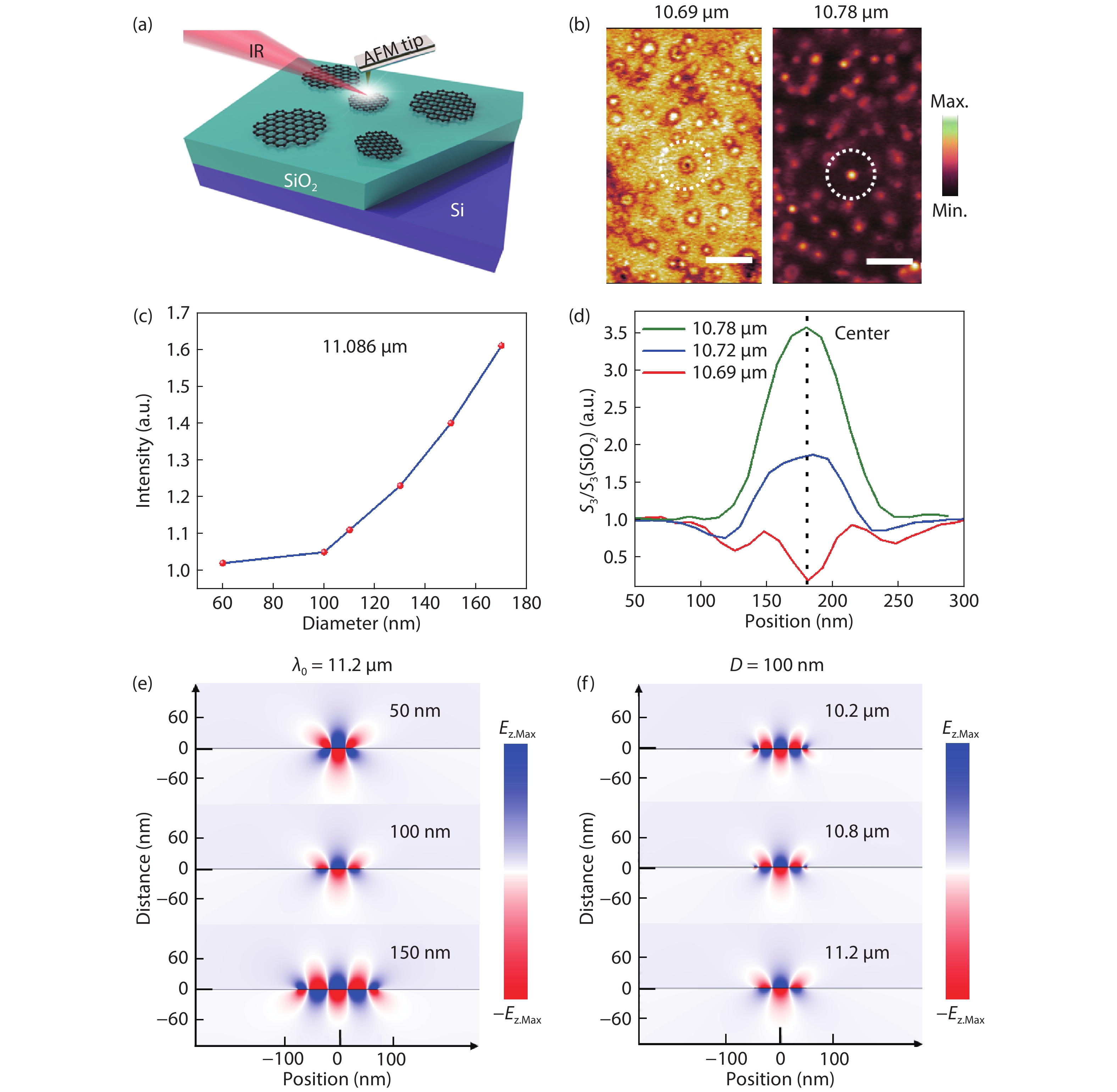
Hillenbrand R, Taubner T, Keilmann F. Phonon-enhanced light–matter interaction at the nanometre scale. Nature, 2002, 418, 159 doi: 10.1038/nature00899 |
| [26] |
|
| [27] |
Novotny L, Hecht B. Principles of nano-optics. Cambridge: Cambridge University Press, 2009
|
| [28] |
Khurgin J B, Boltasseva A. Reflecting upon the losses in plasmonics and metamaterials. MRS Bull, 2012, 37, 768 doi: 10.1557/mrs.2012.173 |
| [29] |
Khurgin J B, Sun G. In search of the elusive lossless metal. Appl Phys Lett, 2010, 96, 181102 doi: 10.1063/1.3425890 |
| [30] |
Chen J N, Badioli M, Alonso-González P, et al. Optical nano-imaging of gate-tunable graphene plasmons. Nature, 2012, 487, 77 doi: 10.1038/nature11254 |
| [31] |
Fei Z, Rodin A S, Andreev G O, et al. Gate-tuning of graphene plasmons revealed by infrared nano-imaging. Nature, 2012, 487, 82 doi: 10.1038/nature11253 |
| [32] |
Ni G X, McLeod A S, Sun Z, et al. Fundamental limits to graphene plasmonics. Nature, 2018, 557, 530 doi: 10.1038/s41586-018-0136-9 |
| [33] |
Fang Z Y, Wang Y M, Schlather A E, et al. Active tunable absorption enhancement with graphene nanodisk arrays. Nano Lett, 2014, 14, 299 doi: 10.1021/nl404042h |
| [34] |
Yan H G, Low T, Zhu W J, et al. Damping pathways of mid-infrared plasmons in graphene nanostructures. Nat Photonics, 2013, 7, 394 doi: 10.1038/nphoton.2013.57 |
| [35] |
Nikitin A Y, Alonso-González P, Vélez S, et al. Real-space mapping of tailored sheet and edge plasmons in graphene nanoresonators. Nat Photonics, 2016, 10, 239 doi: 10.1038/nphoton.2016.44 |
| [36] |
Yang X X, Zhai F, Hu H, et al. Far-field spectroscopy and near-field optical imaging of coupled plasmon-phonon polaritons in 2D van der waals heterostructures. Adv Mater, 2016, 28, 2931 doi: 10.1002/adma.201505765 |
| [37] |
Xu Q Y, Ma T, Danesh M, et al. Effects of edge on graphene plasmons as revealed by infrared nanoimaging. Light: Sci Appl, 2017, 6, e16204 doi: 10.1038/lsa.2016.204 |
| [38] |
Liu D H, Chen X S, Hu Y B, et al. Raman enhancement on ultra-clean graphene quantum dots produced by quasi-equilibrium plasma-enhanced chemical vapor deposition. Nat Commun, 2018, 9, 193 doi: 10.1038/s41467-017-02627-5 |
| [39] |
Chen X Z, Hu D B, Mescall R, et al. Modern scattering-type scanning near-field optical microscopy for advanced material research. Adv Mater, 2019, 31, 1804774 doi: 10.1002/adma.201804774 |


 DownLoad: