J. Semicond. > 2021, Volume 42 > Issue 11 > 112002

ARTICLES

Radiation-hardened property of single-walled carbon nanotube film-based field-effect transistors under low-energy proton irradiation

Xiaorui Zhang1, 3, Huiping Zhu2, Song’ang Peng1, 2, Guodong Xiong2, 3, Chaoyi Zhu1, 3, Xinnan Huang1, 3, Shurui Cao1, 3, Junjun Zhang2, 3, Yunpeng Yan1, 3, Yao Yao1, 4, Dayong Zhang1, Jingyuan Shi1, Lei Wang2, Bo Li2 and Zhi Jin1,

+ Author Affiliations

 Corresponding author: Zhi Jin, jinzhi@ime.ac.cn

DOI: 10.1088/1674-4926/42/11/112002

PDF

Turn off MathJax

Abstract: Strong C–C bonds, nanoscale cross-section and low atomic number make single-walled carbon nanotubes (SWCNTs) a potential candidate material for integrated circuits (ICs) applied in outer space. However, very little work combines the simulation calculations with the electrical measurements of SWCNT field-effect transistors (FETs), which limits further understanding on the mechanisms of radiation effects. Here, SWCNT film-based FETs were fabricated to explore the total ionizing dose (TID) and displacement damage effect on the electrical performance under low-energy proton irradiation with different fluences up to 1 × 10¹⁵ p/cm2. Large negative shift of the threshold voltage and obvious decrease of the on-state current verified the TID effect caused in the oxide layer. The stability of the subthreshold swing and the off-state current reveals that the displacement damage caused in the CNT layer is not serious, which proves that the CNT film is radiation-hardened. Specially, according to the simulation, we found the displacement damage caused by protons is different in the source/drain contact area and channel area, leading to varying degrees of change for the contact resistance and sheet resistance. Having analyzed the simulation results and electrical measurements, we explained the low-energy proton irradiation mechanism of the CNT FETs, which is essential for the construction of radiation-hardened CNT film-based ICs for aircrafts.

Key words: SWCNT FETslow-energy proton irradiationradiation effectselectrical performanceTID effectdisplacement damage effectsimulation


[1]
Akinwande D, Huyghebaert C, Wang C H, et al. Graphene and two-dimensional materials for silicon technology. Nature, 2019, 573, 507 doi: 10.1038/s41586-019-1573-9
[2]
Tulevski G S, Franklin A D, Frank D, et al. Toward high-performance digital logic technology with carbon nanotubes. ACS Nano, 2014, 8, 8730 doi: 10.1021/nn503627h
[3]
Chau R, Datta S, Doczy M, et al. Benchmarking nanotechnology for high-performance and low-power logic transistor applications. IEEE Trans Nanotechnol, 2005, 4, 153 doi: 10.1109/TNANO.2004.842073
[4]
Franklin A D. The road to carbon nanotube transistors. Nature, 2013, 498, 443 doi: 10.1038/498443a
[5]
Liu L J, Han J, Xu L, et al. Aligned, high-density semiconducting carbon nanotube arrays for high-performance electronics. Science, 2020, 368, 850 doi: 10.1126/science.aba5980
[6]
McMorrow J J, Cress C D, Gaviria Rojas W A, et al. Radiation-hard complementary integrated circuits based on semiconducting single-walled carbon nanotubes. ACS Nano, 2017, 11, 2992 doi: 10.1021/acsnano.6b08561
[7]
Krasheninnikov A V, Nordlund K. Ion and electron irradiation-induced effects in nanostructured materials. J Appl Phys, 2010, 107, 071301 doi: 10.1063/1.3318261
[8]
Zhu M G, Zhang Z Y, Peng L M. High-performance and radiation-hard carbon nanotube complementary static random-access memory. Adv Electron Mater, 2019, 5, 1900313 doi: 10.1002/aelm.201900313
[9]
Francis S A, Cress C D, McClory J W, et al. Characterization of radiation damage in carbon nanotube field-effect transistors. IEEE Trans Nucl Sci, 2013, 60, 4087 doi: 10.1109/TNS.2013.2284542
[10]
Zhang C X, Zhang E, Fleetwood D M, et al. Total-ionizing-dose effects and reliability of carbon nanotube FET devices. Microelectron Reliab, 2014, 54, 2355 doi: 10.1016/j.microrel.2014.05.011
[11]
Cress C D, McMorrow J J, Robinson J T, et al. Radiation effects in single-walled carbon nanotube thin-film-transistors. IEEE Trans Nucl Sci, 2010, 57, 3040 doi: 10.1063/1.3268470
[12]
Peck D S, Schmid E R. Effects of radiation on transistors in the first telstar satellite. Nature, 1963, 199, 741 doi: 10.1038/199741a0
[13]
Fleetwood D M. Evolution of total ionizing dose effects in MOS devices with Moore's law scaling. IEEE Trans Nucl Sci, 2018, 65, 1465 doi: 10.1109/TNS.2017.2786140
[14]
Summers G P, Messenger S R, Burke E A, et al. Low energy proton-induced displacement damage in shielded GaAs solar cells in space. Appl Phys Lett, 1997, 71, 832 doi: 10.1063/1.119660
[15]
Xiong G D, Qin Z L, Li B, et al. Radiation hardness and abnormal photoresponse dynamics of the CH3NH3PbI3 perovskite photodetector. J Mater Chem C, 2021, 9, 2095 doi: 10.1039/D0TC05148A
[16]
Schwank J R, Shaneyfelt M R, Dodd P E. Radiation hardness assurance testing of microelectronic devices and integrated circuits: Radiation environments, physical mechanisms, and foundations for hardness assurance. IEEE Trans Nucl Sci, 2013, 60, 2074 doi: 10.1109/TNS.2013.2254722
[17]
Abbe E, Schüler T, Klosz S, et al. Electrical behaviour of carbon nanotubes under low-energy proton irradiation. J Nucl Mater, 2017, 495, 299 doi: 10.1016/j.jnucmat.2017.08.032
[18]
Hong W K, Lee C, Nepal D, et al. Radiation hardness of the electrical properties of carbon nanotube network field effect transistors under high-energy proton irradiation. Nanotechnology, 2006, 17, 5675 doi: 10.1088/0957-4484/17/22/023
[19]
Nelson A J, Baby L, Boroujeni A Y, et al. Effect of proton irradiation on the electrical resistivity of carbon nanotube-epoxy composites. Nanosci Nanotechnol Lett, 2015, 7, 157 doi: 10.1166/nnl.2015.1898
[20]
Ishii S, Toki J, Oikawa M, et al. Electrical responses of a carbon nanotube thin-film transistor to MeV proton irradiation in air. Radiat Eff Defects Solids, 2020, 175, 440 doi: 10.1080/10420150.2019.1671386
[21]
Gigax J G, Bradford P D, Shao L. Radiation-induced mechanical property changes of CNT yarn. Nucl Instrum Methods Phys Res Sect B, 2017, 409, 268 doi: 10.1016/j.nimb.2017.04.050
[22]
Ziegler J F, Ziegler M D, Biersack J P. SRIM – The stopping and range of ions in matter (2010). Nucl Instrum Methods Phys Res Sect B, 2010, 268, 1818 doi: 10.1016/j.nimb.2010.02.091
[23]
Allison J, Amako K, Apostolakis J, et al. Recent developments in Geant4. Nucl Instrum Methods Phys Resh Sect A, 2016, 835, 186 doi: 10.1016/j.nima.2016.06.125
[24]
Zhang J J, Liu F Y, Li B, et al. Single event upset for monolithic 3-D integrated 6T SRAM based on a 22 nm FD-SOI technology: Effects of channel size and temperature. Microelectron Reliab, 2020, 114, 113783 doi: 10.1016/j.microrel.2020.113783
[25]
Kim W, Javey A, Vermesh O, et al. Hysteresis caused by water molecules in carbon nanotube field-effect transistors. Nano Lett, 2003, 3, 193 doi: 10.1021/nl0259232
[26]
Lee S, Peng J W. Effect of plasma treatment on electrical conductivity and Raman spectra of carbon nanotubes. J Phys Chem Solids, 2011, 72, 1101 doi: 10.1016/j.jpcs.2011.06.012
[27]
Kim D W, Lee K W, Choi D M, et al. Raman spectroscopy of proton-irradiated octadecylamine-functionalized carbon nanotube films. J Korean Phys Soc, 2015, 67, 608 doi: 10.3938/jkps.67.608
[28]
Anelli G, Campbell M, Delmastro M, et al. Radiation tolerant VLSI circuits in standard deep submicron CMOS technologies for the LHC experiments: Practical design aspects. IEEE Trans Nucl Sci, 1999, 46, 1690 doi: 10.1109/23.819140
[29]
Chang H Y, Zhu W N, Akinwande D. On the mobility and contact resistance evaluation for transistors based on MoS2 or two-dimensional semiconducting atomic crystals. Appl Phys Lett, 2014, 104, 113504 doi: 10.1063/1.4868536
[30]
Ghibaudo G. New method for the extraction of MOSFET parameters. Electron Lett, 1988, 24, 543 doi: 10.1049/el:19880369
[31]
Schwank J R, Shaneyfelt M R, Fleetwood D M, et al. Radiation effects in MOS oxides. IEEE Trans Nucl Sci, 2008, 55, 1833 doi: 10.1109/TNS.2008.2001040
[32]
Zhao Y D, Li D Q, Xiao L, et al. Radiation effects and radiation hardness solutions for single-walled carbon nanotube-based thin film transistors and logic devices. Carbon, 2016, 108, 363 doi: 10.1016/j.carbon.2016.07.033
[33]
He Y, Zhang J Y, Hou S M, et al. Schottky barrier formation at metal electrodes and semiconducting carbon nanotubes. Appl Phys Lett, 2009, 94, 093107 doi: 10.1063/1.3093677
[34]
Banhart F. Interactions between metals and carbon nanotubes: At the interface between old and new materials. Nanoscale, 2009, 1, 201 doi: 10.1039/b9nr00127a
[35]
Cress C D, McMorrow J J, Robinson J T, et al. Total ionizing dose-hardened carbon nanotube thin-film transistors with silicon oxynitride gate dielectrics. MRS Commun, 2011, 1, 27 doi: 10.1557/mrc.2011.10
[36]
Schwank J R, Winokur P S, Sexton F W, et al. Radiation-induced interface-state generation in MOS devices. IEEE Trans Nucl Sci, 1986, 33, 1177 doi: 10.1109/TNS.1986.4334575
[37]
Huang X N, Yao Y, Peng S, et al. Effects of charge trapping at the MoS2–SiO2 interface on the stability of subthreshold swing of MoS2 field effect transistors. Materials, 2020, 13, 2896 doi: 10.3390/ma13132896
[38]
Huang X N, Shi J Y, Yao Y, et al. Layer thickness influenced irradiation effects of proton beam on MoS2 field effect transistors. Nanotechnology, 2021, 32, 135204 doi: 10.1088/1361-6528/abd129
[39]
Yao Y, Peng S A, Huang X N, et al. A uniform stable P-type graphene doping method with a gold etching process. Nanotechnology, 2019, 30, 405205 doi: 10.1088/1361-6528/ab2e33
[40]
Peng S A, Jin Z, Ma P, et al. The sheet resistance of graphene under contact and its effect on the derived specific contact resistivity. Carbon, 2015, 82, 500 doi: 10.1016/j.carbon.2014.11.001
[41]
Peng S, Jin Z, Yao Y, et al. Controllable p-to-n type conductance transition in top-gated graphene field effect transistor by interface trap engineering. Adv Electron Mater, 2020, 6, 2000496 doi: 10.1002/aelm.202000496
[42]
Peng S A, Jin Z, Zhang D Y, et al. How do contact and channel contribute to the Dirac points in graphene field-effect transistors. Adv Electron Mater, 2018, 4, 1800158 doi: 10.1002/aelm.201800158
[43]
Peng S, Jin Z, Zhang D Y, et al. Carrier-number-fluctuation induced ultralow 1/f noise level in top-gated graphene field effect transistor. ACS Appl Mater Interfaces, 2017, 9, 6661 doi: 10.1021/acsami.6b15862
[44]
Peng S, Jin Z, Zhang D, et al. Evidence of electric field-tunable tunneling probability in graphene and metal contact. Nanoscale, 2017, 9, 9520 doi: 10.1039/C7NR02502E
[45]
Peng S, Jin Z, Yao Y, et al. Metal-contact-induced transition of electrical transport in monolayer MoS2: From thermally activated to variable-range hopping. Adv Electron Mater, 2019, 5, 1900042 doi: 10.1002/aelm.201900042
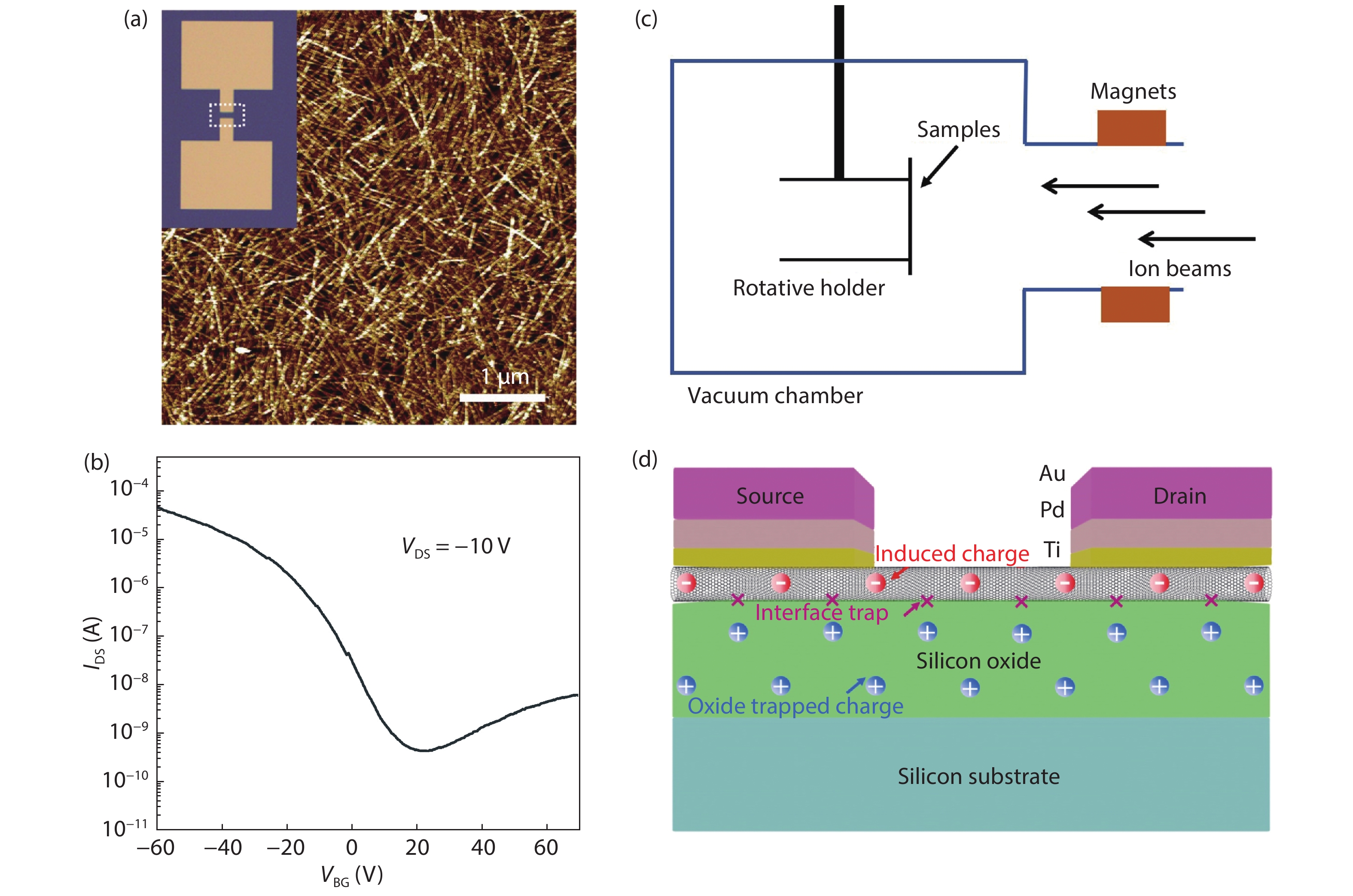
Fig. 1.  (Color online) Structure and properties of the SWCNT-film-based FET. (a) AFM morphologic image showing the SWCNT film deposited on the Si/SiO2 substrate. The inset is the optical image of a SWCNT FET, of which the channel length is 10 μm and the width is 20 μm. (b) Typical transfer charateristics curves of the SWCNT FET before irradiation at VDS = –10 V. (c) Schematic diagram of the low-energy charged particle irradiation simulation test device composed of an ionization chamber, accelerator and irradiation chamber. (d) Schematic showing the total ionizing dose (TID) and displacement damage effect in the SWCNT FET induced by proton irradiation.

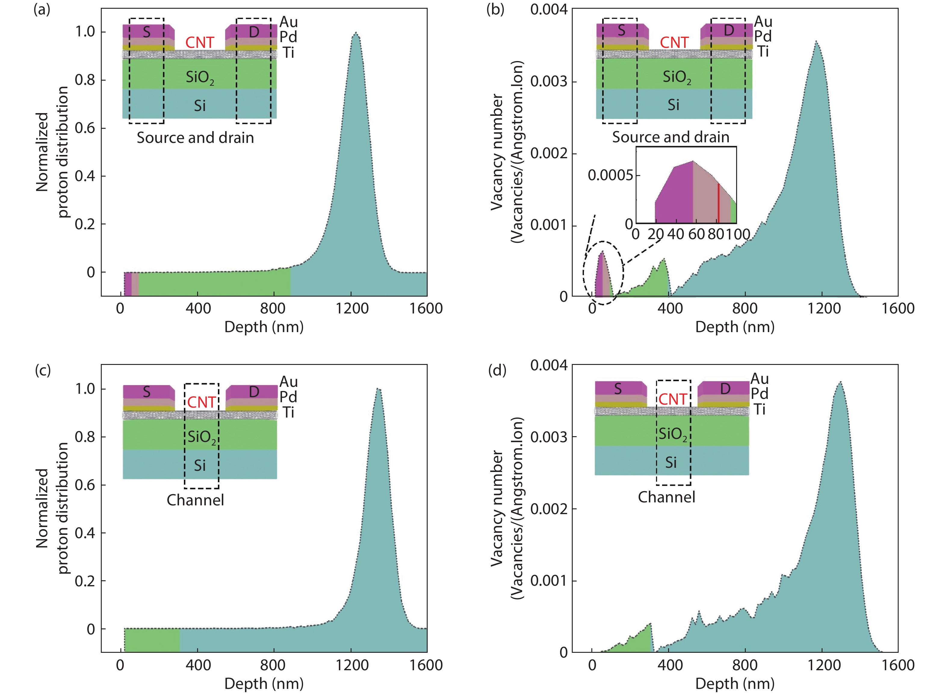
Fig. 2.  (Color online) Simulation results of (a) the distribution of protons in the source/drain region (Au/Pd/Ti/SWCNT/SiO2/Si), (b) the number of vacancies in the source/drain region (Au/Pd/Ti/SWCNT/SiO2/Si), (c) distribution of protons in the channel region (SWCNT/SiO2/Si), and (d) the number of vacancies in the channel region (SWCNT/SiO2/Si) by SRIM. The energy of the protons is 150 keV. The inset is the illustration of the simulation region, including the source/drain contact region and the SWCNT channel region.

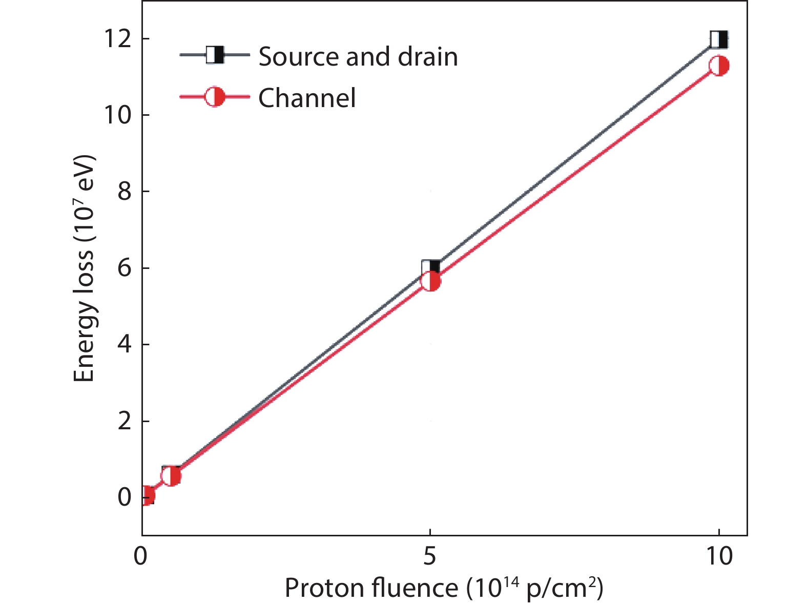
Fig. 3.  Simulation result of the energy loss in the metal/CNT contact and channel region of the CNT-layer performed by GEANT 4 with four different proton irradiation fluences of 5 × 10¹², 5 × 10¹³, 5 × 10¹⁴ and 1 × 10¹⁵ p/cm2.

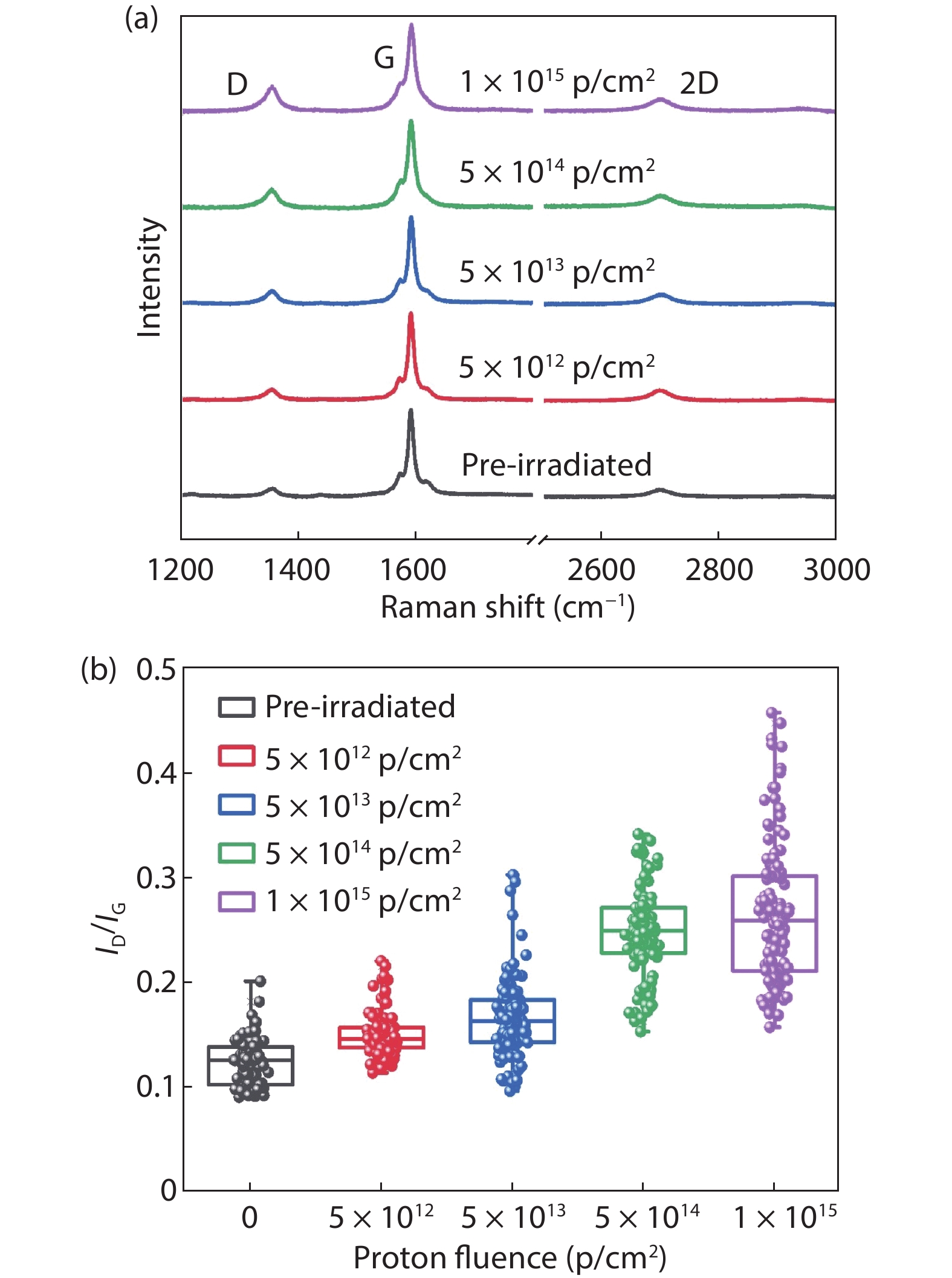
Fig. 4.  Raman spectra of SWCNT FETs before and after proton irradiation with four different proton fluences of 5 × 10¹², 5 × 10¹³, 5 × 10¹⁴ and 1 × 10¹⁵ p/cm2. (a) Single point Raman spectra of SWCNT FETs with different proton fluences, in which the G peaks are normalized. (b) Statistical study on the ratio of the D peak intensity to the G peak intensity (ID/IG) with different proton fluences. Each sample has 121 test points, which are obtained by Raman mapping. The test area is 5 × 5 μm2 and the spacing is 0.5 μm.

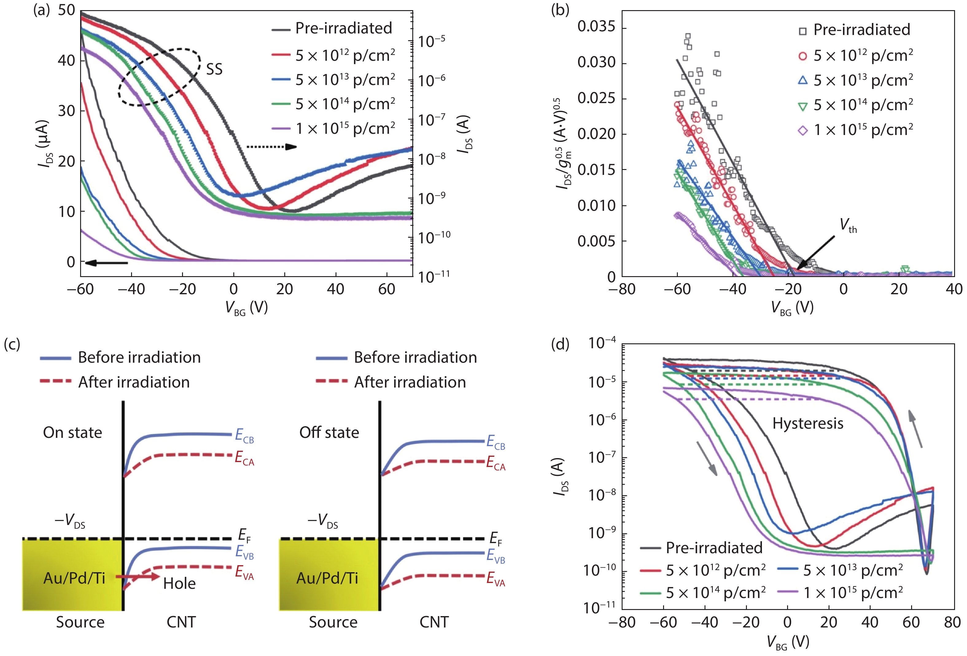
Fig. 5.  (Color online) (a) Typical transfer characteristics curves of the SWCNT FETs at VDS = –10 V with different proton fluences. (b) Threshold voltage (Vth) values extracted by the Y-function method with different proton fluences. (c) Band structure of SWCNT with metal before and after proton irradiation at the on- (left) and off-state (right). (d) Hysteresis in typical transfer characteristics curves with different proton fluences at VDS = –10 V.

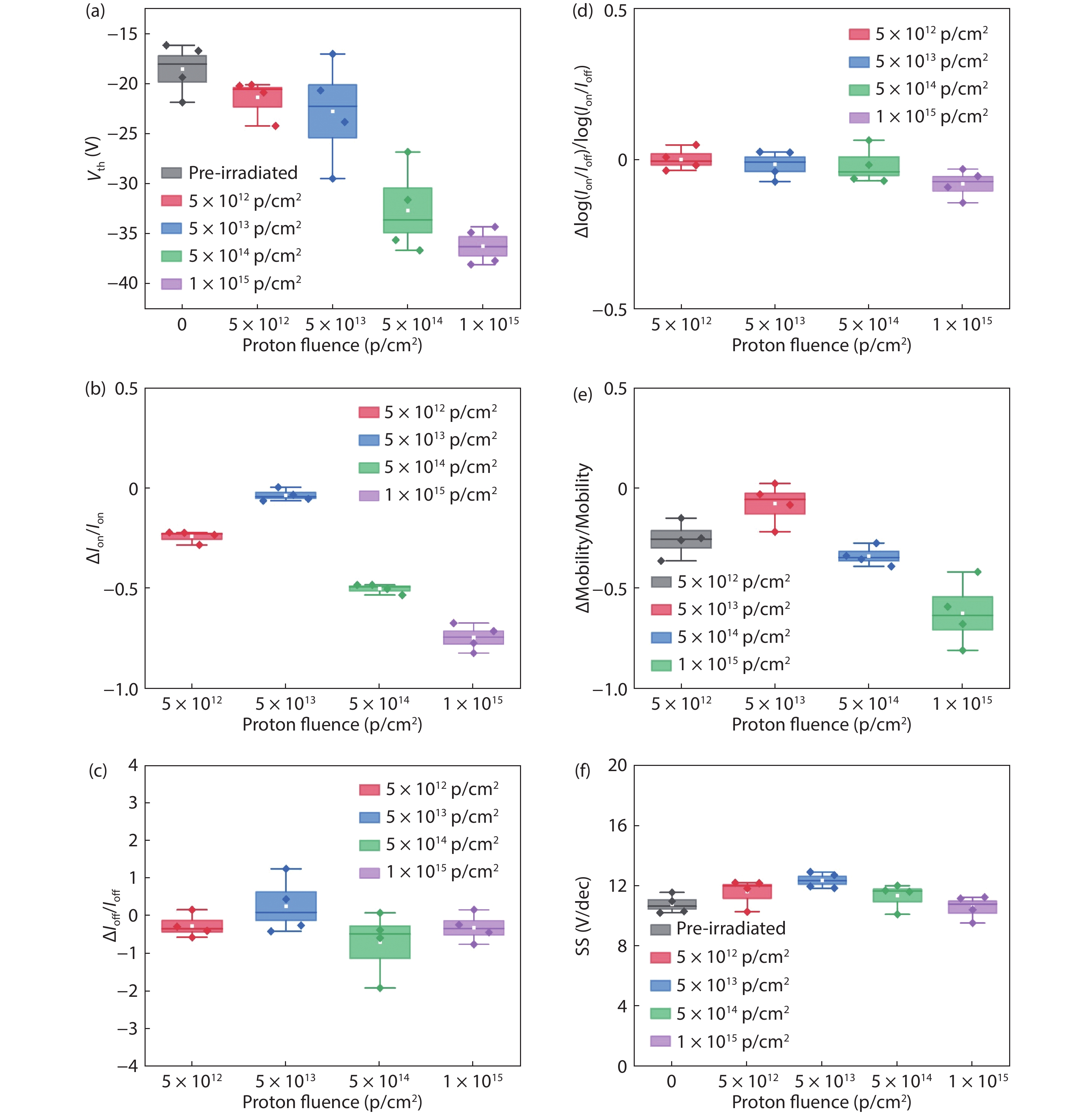
Fig. 6.  Statistics measurements of (a) the threshold voltage (Vth), (b) rate of on-current (Ion) change, (c) rate of off-current (Ioff) change, (d) rate of on/off ratio change, (e) rate of mobility change, and (f) subthreshold swing (SS) with four different proton irradiation fluences of 5 × 10¹², 5 × 10¹³, 5 × 10¹⁴ and 1 × 10¹⁵ p/cm2.

Fig. 7.  (Color online) TLM measurements of SWCNT FETs before and after proton irradiation with four different proton fluences of 5 × 10¹², 5 × 10¹³, 5 × 10¹⁴ and 1 × 10¹⁵ p/cm2. (a) Typical current–voltage curves of a complete SWCNT TLM test structure before proton irradiation at VBG = –10 V. Inset is the optical image of a SWCNT TLM test structure consisting of several FETs, which have the same channel width (7 μm) and different channel length (4, 6, 10, 14, 18, 22, 28 and 35 μm, respectively). (b) Length-dependent total resistances of SWCNT FETs with different proton fluences.

[1]
Akinwande D, Huyghebaert C, Wang C H, et al. Graphene and two-dimensional materials for silicon technology. Nature, 2019, 573, 507 doi: 10.1038/s41586-019-1573-9
[2]
Tulevski G S, Franklin A D, Frank D, et al. Toward high-performance digital logic technology with carbon nanotubes. ACS Nano, 2014, 8, 8730 doi: 10.1021/nn503627h
[3]
Chau R, Datta S, Doczy M, et al. Benchmarking nanotechnology for high-performance and low-power logic transistor applications. IEEE Trans Nanotechnol, 2005, 4, 153 doi: 10.1109/TNANO.2004.842073
[4]
Franklin A D. The road to carbon nanotube transistors. Nature, 2013, 498, 443 doi: 10.1038/498443a
[5]
Liu L J, Han J, Xu L, et al. Aligned, high-density semiconducting carbon nanotube arrays for high-performance electronics. Science, 2020, 368, 850 doi: 10.1126/science.aba5980
[6]
McMorrow J J, Cress C D, Gaviria Rojas W A, et al. Radiation-hard complementary integrated circuits based on semiconducting single-walled carbon nanotubes. ACS Nano, 2017, 11, 2992 doi: 10.1021/acsnano.6b08561
[7]
Krasheninnikov A V, Nordlund K. Ion and electron irradiation-induced effects in nanostructured materials. J Appl Phys, 2010, 107, 071301 doi: 10.1063/1.3318261
[8]
Zhu M G, Zhang Z Y, Peng L M. High-performance and radiation-hard carbon nanotube complementary static random-access memory. Adv Electron Mater, 2019, 5, 1900313 doi: 10.1002/aelm.201900313
[9]
Francis S A, Cress C D, McClory J W, et al. Characterization of radiation damage in carbon nanotube field-effect transistors. IEEE Trans Nucl Sci, 2013, 60, 4087 doi: 10.1109/TNS.2013.2284542
[10]
Zhang C X, Zhang E, Fleetwood D M, et al. Total-ionizing-dose effects and reliability of carbon nanotube FET devices. Microelectron Reliab, 2014, 54, 2355 doi: 10.1016/j.microrel.2014.05.011
[11]
Cress C D, McMorrow J J, Robinson J T, et al. Radiation effects in single-walled carbon nanotube thin-film-transistors. IEEE Trans Nucl Sci, 2010, 57, 3040 doi: 10.1063/1.3268470
[12]
Peck D S, Schmid E R. Effects of radiation on transistors in the first telstar satellite. Nature, 1963, 199, 741 doi: 10.1038/199741a0
[13]
Fleetwood D M. Evolution of total ionizing dose effects in MOS devices with Moore's law scaling. IEEE Trans Nucl Sci, 2018, 65, 1465 doi: 10.1109/TNS.2017.2786140
[14]
Summers G P, Messenger S R, Burke E A, et al. Low energy proton-induced displacement damage in shielded GaAs solar cells in space. Appl Phys Lett, 1997, 71, 832 doi: 10.1063/1.119660
[15]
Xiong G D, Qin Z L, Li B, et al. Radiation hardness and abnormal photoresponse dynamics of the CH3NH3PbI3 perovskite photodetector. J Mater Chem C, 2021, 9, 2095 doi: 10.1039/D0TC05148A
[16]
Schwank J R, Shaneyfelt M R, Dodd P E. Radiation hardness assurance testing of microelectronic devices and integrated circuits: Radiation environments, physical mechanisms, and foundations for hardness assurance. IEEE Trans Nucl Sci, 2013, 60, 2074 doi: 10.1109/TNS.2013.2254722
[17]
Abbe E, Schüler T, Klosz S, et al. Electrical behaviour of carbon nanotubes under low-energy proton irradiation. J Nucl Mater, 2017, 495, 299 doi: 10.1016/j.jnucmat.2017.08.032
[18]
Hong W K, Lee C, Nepal D, et al. Radiation hardness of the electrical properties of carbon nanotube network field effect transistors under high-energy proton irradiation. Nanotechnology, 2006, 17, 5675 doi: 10.1088/0957-4484/17/22/023
[19]
Nelson A J, Baby L, Boroujeni A Y, et al. Effect of proton irradiation on the electrical resistivity of carbon nanotube-epoxy composites. Nanosci Nanotechnol Lett, 2015, 7, 157 doi: 10.1166/nnl.2015.1898
[20]
Ishii S, Toki J, Oikawa M, et al. Electrical responses of a carbon nanotube thin-film transistor to MeV proton irradiation in air. Radiat Eff Defects Solids, 2020, 175, 440 doi: 10.1080/10420150.2019.1671386
[21]
Gigax J G, Bradford P D, Shao L. Radiation-induced mechanical property changes of CNT yarn. Nucl Instrum Methods Phys Res Sect B, 2017, 409, 268 doi: 10.1016/j.nimb.2017.04.050
[22]
Ziegler J F, Ziegler M D, Biersack J P. SRIM – The stopping and range of ions in matter (2010). Nucl Instrum Methods Phys Res Sect B, 2010, 268, 1818 doi: 10.1016/j.nimb.2010.02.091
[23]
Allison J, Amako K, Apostolakis J, et al. Recent developments in Geant4. Nucl Instrum Methods Phys Resh Sect A, 2016, 835, 186 doi: 10.1016/j.nima.2016.06.125
[24]
Zhang J J, Liu F Y, Li B, et al. Single event upset for monolithic 3-D integrated 6T SRAM based on a 22 nm FD-SOI technology: Effects of channel size and temperature. Microelectron Reliab, 2020, 114, 113783 doi: 10.1016/j.microrel.2020.113783
[25]
Kim W, Javey A, Vermesh O, et al. Hysteresis caused by water molecules in carbon nanotube field-effect transistors. Nano Lett, 2003, 3, 193 doi: 10.1021/nl0259232
[26]
Lee S, Peng J W. Effect of plasma treatment on electrical conductivity and Raman spectra of carbon nanotubes. J Phys Chem Solids, 2011, 72, 1101 doi: 10.1016/j.jpcs.2011.06.012
[27]
Kim D W, Lee K W, Choi D M, et al. Raman spectroscopy of proton-irradiated octadecylamine-functionalized carbon nanotube films. J Korean Phys Soc, 2015, 67, 608 doi: 10.3938/jkps.67.608
[28]
Anelli G, Campbell M, Delmastro M, et al. Radiation tolerant VLSI circuits in standard deep submicron CMOS technologies for the LHC experiments: Practical design aspects. IEEE Trans Nucl Sci, 1999, 46, 1690 doi: 10.1109/23.819140
[29]
Chang H Y, Zhu W N, Akinwande D. On the mobility and contact resistance evaluation for transistors based on MoS2 or two-dimensional semiconducting atomic crystals. Appl Phys Lett, 2014, 104, 113504 doi: 10.1063/1.4868536
[30]
Ghibaudo G. New method for the extraction of MOSFET parameters. Electron Lett, 1988, 24, 543 doi: 10.1049/el:19880369
[31]
Schwank J R, Shaneyfelt M R, Fleetwood D M, et al. Radiation effects in MOS oxides. IEEE Trans Nucl Sci, 2008, 55, 1833 doi: 10.1109/TNS.2008.2001040
[32]
Zhao Y D, Li D Q, Xiao L, et al. Radiation effects and radiation hardness solutions for single-walled carbon nanotube-based thin film transistors and logic devices. Carbon, 2016, 108, 363 doi: 10.1016/j.carbon.2016.07.033
[33]
He Y, Zhang J Y, Hou S M, et al. Schottky barrier formation at metal electrodes and semiconducting carbon nanotubes. Appl Phys Lett, 2009, 94, 093107 doi: 10.1063/1.3093677
[34]
Banhart F. Interactions between metals and carbon nanotubes: At the interface between old and new materials. Nanoscale, 2009, 1, 201 doi: 10.1039/b9nr00127a
[35]
Cress C D, McMorrow J J, Robinson J T, et al. Total ionizing dose-hardened carbon nanotube thin-film transistors with silicon oxynitride gate dielectrics. MRS Commun, 2011, 1, 27 doi: 10.1557/mrc.2011.10
[36]
Schwank J R, Winokur P S, Sexton F W, et al. Radiation-induced interface-state generation in MOS devices. IEEE Trans Nucl Sci, 1986, 33, 1177 doi: 10.1109/TNS.1986.4334575
[37]
Huang X N, Yao Y, Peng S, et al. Effects of charge trapping at the MoS2–SiO2 interface on the stability of subthreshold swing of MoS2 field effect transistors. Materials, 2020, 13, 2896 doi: 10.3390/ma13132896
[38]
Huang X N, Shi J Y, Yao Y, et al. Layer thickness influenced irradiation effects of proton beam on MoS2 field effect transistors. Nanotechnology, 2021, 32, 135204 doi: 10.1088/1361-6528/abd129
[39]
Yao Y, Peng S A, Huang X N, et al. A uniform stable P-type graphene doping method with a gold etching process. Nanotechnology, 2019, 30, 405205 doi: 10.1088/1361-6528/ab2e33
[40]
Peng S A, Jin Z, Ma P, et al. The sheet resistance of graphene under contact and its effect on the derived specific contact resistivity. Carbon, 2015, 82, 500 doi: 10.1016/j.carbon.2014.11.001
[41]
Peng S, Jin Z, Yao Y, et al. Controllable p-to-n type conductance transition in top-gated graphene field effect transistor by interface trap engineering. Adv Electron Mater, 2020, 6, 2000496 doi: 10.1002/aelm.202000496
[42]
Peng S A, Jin Z, Zhang D Y, et al. How do contact and channel contribute to the Dirac points in graphene field-effect transistors. Adv Electron Mater, 2018, 4, 1800158 doi: 10.1002/aelm.201800158
[43]
Peng S, Jin Z, Zhang D Y, et al. Carrier-number-fluctuation induced ultralow 1/f noise level in top-gated graphene field effect transistor. ACS Appl Mater Interfaces, 2017, 9, 6661 doi: 10.1021/acsami.6b15862
[44]
Peng S, Jin Z, Zhang D, et al. Evidence of electric field-tunable tunneling probability in graphene and metal contact. Nanoscale, 2017, 9, 9520 doi: 10.1039/C7NR02502E
[45]
Peng S, Jin Z, Yao Y, et al. Metal-contact-induced transition of electrical transport in monolayer MoS2: From thermally activated to variable-range hopping. Adv Electron Mater, 2019, 5, 1900042 doi: 10.1002/aelm.201900042
1

Displacement damage effects in MoS2-based electronics

Kaiyue He, Zhanqi Li, Taotao Li, Yifu Sun, Shitong Zhu, et al.

Journal of Semiconductors, 2024, 45(12): 122701. doi: 10.1088/1674-4926/24090027

2

The effect of γ-ray irradiation on the SOT magnetic films and Hall devices

Tengzhi Yang, Yan Cui, Yanru Li, Meiyin Yang, Jing Xu, et al.

Journal of Semiconductors, 2021, 42(2): 024102. doi: 10.1088/1674-4926/42/2/024102

3

Simulation of double junction In0.46Ga0.54N/Si tandem solar cell

M. Benaicha, L. Dehimi, Nouredine Sengouga

Journal of Semiconductors, 2017, 38(4): 044002. doi: 10.1088/1674-4926/38/4/044002

4

Effect of metal-fingers/doped-ZnO transparent electrode on performance of GaN/InGaN solar cell

S.R. Routray, T.R. Lenka

Journal of Semiconductors, 2017, 38(9): 092001. doi: 10.1088/1674-4926/38/9/092001

5

Study of the effect of switching speed of the a-SiC/c-Si (p)-based, thyristor-like, ultra-high-speed switches, using two-dimensional simulation techniques

Evangelos I. Dimitriadis, Nikolaos Georgoulas

Journal of Semiconductors, 2017, 38(5): 054001. doi: 10.1088/1674-4926/38/5/054001

6

Modeling and simulation of single-event effect in CMOS circuit

Suge Yue, Xiaolin Zhang, Yuanfu Zhao, Lin Liu

Journal of Semiconductors, 2015, 36(11): 111002. doi: 10.1088/1674-4926/36/11/111002

7

Electro-magnetic weak coupling optical polaron and temperature effect in quantum dot

M. Tiotsop, A. J. Fotue, S. C. Kenfack, N. Issofa, A. V. Wirngo, et al.

Journal of Semiconductors, 2015, 36(10): 102001. doi: 10.1088/1674-4926/36/10/102001

8

Effect of electric field on metallic SWCNT interconnects for nanoscale technologies

Harsimran Kaur, Karamjit Singh Sandha

Journal of Semiconductors, 2015, 36(3): 035001. doi: 10.1088/1674-4926/36/3/035001

9

Effects of interface trap density on the electrical performance of amorphous InSnZnO thin-film transistor

Yongye Liang, Kyungsoo Jang, S. Velumani, Cam Phu Thi Nguyen, Junsin Yi, et al.

Journal of Semiconductors, 2015, 36(2): 024007. doi: 10.1088/1674-4926/36/2/024007

10

Effect of band gap energy on the electrical conductivity in doped ZnO thin film

Said Benramache, Okba Belahssen, Hachemi Ben Temam

Journal of Semiconductors, 2014, 35(7): 073001. doi: 10.1088/1674-4926/35/7/073001

11

Simulation study on short channel double-gate junctionless field-effect transistors

Meile Wu, Xiaoshi Jin, Rongyan Chuai, Xi Liu, Jong-Ho Lee, et al.

Journal of Semiconductors, 2013, 34(3): 034004. doi: 10.1088/1674-4926/34/3/034004

12

Modeling and simulation of centroid and inversion charge density in cylindrical surrounding gate MOSFETs including quantum effects

P. Vimala, N. B. Balamurugan

Journal of Semiconductors, 2013, 34(11): 114001. doi: 10.1088/1674-4926/34/11/114001

13

The effects of electron irradiation on the optical properties of the organic semiconductor polypyrrole

J. V. Thombare, M. C. Rath, S. H. Han, V. J. Fulari

Journal of Semiconductors, 2013, 34(9): 093001. doi: 10.1088/1674-4926/34/9/093001

14

A simulation of doping and trap effects on the spectral response of AlGaN ultraviolet detectors

Sidi Ould Saad Hamady

Journal of Semiconductors, 2012, 33(3): 034002. doi: 10.1088/1674-4926/33/3/034002

15

Radiation effect on the optical and electrical properties of CdSe(In)/p-Si heterojunction photovoltaic solar cells

M. Ashry, S. Fares

Journal of Semiconductors, 2012, 33(10): 102001. doi: 10.1088/1674-4926/33/10/102001

16

Simulation analysis of the effects of a back surface field on a p-a-Si:H/n-c-Si/n+-a-Si:H heterojunction solar cell

Hu Yuehui, Zhang Xiangwen, Qu Minghao, Wang Lifu, Zeng Tao, et al.

Journal of Semiconductors, 2009, 30(6): 064006. doi: 10.1088/1674-4926/30/6/064006

17

Method of simulation of low dose rate for total dose effect in 0.18 μm CMOS technology

He Baoping, Yao Zhibin, Guo Hongxia, Luo Yinhong, Zhang Fengqi, et al.

Journal of Semiconductors, 2009, 30(7): 074009. doi: 10.1088/1674-4926/30/7/074009

18

Experimental Study on Pulse Neutron and Gamma Ray Irradiation Effects on SiGe HBT

Liu Shuhuan, Lin Dongsheng, Guo Xiaoqiang, Liu Hongbing, Jiang Xinbiao, et al.

Chinese Journal of Semiconductors , 2007, 28(1): 78-83.

19

Monte Carlo Simulation of Impurity Scattering Effect in Resonant-Phonon-Assisted Terahertz Quantum-Cascade Lasers

Cao Juncheng, Lü Jingtao

Chinese Journal of Semiconductors , 2006, 27(2): 304-308.

20

Influence of Floating Body Effect on Radiation Hardness of PD SOI nMOSFETs

Zhao Hongchen, Hai Chaohe, Han Zhengsheng,and Qian He

Chinese Journal of Semiconductors , 2005, 26(2): 234-237.

1. Patro, A., Rout, C.S., Dhal, S. et al. Ion beam modification of one-dimensional nano materials: a review. Nanotechnology, 2025, 36(21): 212001. doi:10.1088/1361-6528/adce12
2. Zeng, T., Li, J., Guo, H. et al. X-ray irradiation effects of carbon nanotube field-effect transistors | [碳纳米管场效应晶体管的 X 射线辐照效应]. Wuli Xuebao/Acta Physica Sinica, 2025, 74(5): 058501. doi:10.7498/aps.74.20241670
3. Li, H., Liao, Y., Zhang, F. et al. A Carbon Nanotube Transistor Based on Buried-Gate Structure. Materials, 2025, 18(2): 218. doi:10.3390/ma18020218
4. He, K., Li, Z., Li, T. et al. Displacement damage effects in MoS2-based electronics. Journal of Semiconductors, 2024, 45(12): 122701. doi:10.1088/1674-4926/24090027
5. Kim, S.J., Hwang, S., Kwon, J.-D. et al. Gamma-Irradiation-Induced Electrical Characteristic Variations in MoS2 Field-Effect Transistors with Buried Local Back-Gate Structure. Nanomaterials, 2024, 14(16): 1324. doi:10.3390/nano14161324
6. Liu, J., Li, B., Li, Q. Two-Dimensional Doped Materials. Magnetochemistry, 2022, 8(12): 172. doi:10.3390/magnetochemistry8120172
  • Search

    Advanced Search >>

    GET CITATION

    Xiaorui Zhang, Huiping Zhu, Song’ang Peng, Guodong Xiong, Chaoyi Zhu, Xinnan Huang, Shurui Cao, Junjun Zhang, Yunpeng Yan, Yao Yao, Dayong Zhang, Jingyuan Shi, Lei Wang, Bo Li, Zhi Jin. Radiation-hardened property of single-walled carbon nanotube film-based field-effect transistors under low-energy proton irradiation[J]. Journal of Semiconductors, 2021, 42(11): 112002. doi: 10.1088/1674-4926/42/11/112002
    X R Zhang, H P Zhu, S Peng, G D Xiong, C Y Zhu, X N Huang, S R Cao, J J Zhang, Y P Yan, Y Yao, D Y Zhang, J Y Shi, L Wang, B Li, Z Jin, Radiation-hardened property of single-walled carbon nanotube film-based field-effect transistors under low-energy proton irradiation[J]. J. Semicond., 2021, 42(11): 112002. doi: 10.1088/1674-4926/42/11/112002.
    shu

    Export: BibTex EndNote

    Article Metrics

    Article views: 2685 Times PDF downloads: 91 Times Cited by: 6 Times

    History

    Received: 13 April 2021 Revised: 26 April 2021 Online: Accepted Manuscript: 10 June 2021Uncorrected proof: 18 June 2021Published: 01 November 2021

    Catalog

      Email This Article

      User name:
      Email:*请输入正确邮箱
      Code:*验证码错误
      Xiaorui Zhang, Huiping Zhu, Song’ang Peng, Guodong Xiong, Chaoyi Zhu, Xinnan Huang, Shurui Cao, Junjun Zhang, Yunpeng Yan, Yao Yao, Dayong Zhang, Jingyuan Shi, Lei Wang, Bo Li, Zhi Jin. Radiation-hardened property of single-walled carbon nanotube film-based field-effect transistors under low-energy proton irradiation[J]. Journal of Semiconductors, 2021, 42(11): 112002. doi: 10.1088/1674-4926/42/11/112002 ****X R Zhang, H P Zhu, S Peng, G D Xiong, C Y Zhu, X N Huang, S R Cao, J J Zhang, Y P Yan, Y Yao, D Y Zhang, J Y Shi, L Wang, B Li, Z Jin, Radiation-hardened property of single-walled carbon nanotube film-based field-effect transistors under low-energy proton irradiation[J]. J. Semicond., 2021, 42(11): 112002. doi: 10.1088/1674-4926/42/11/112002.
      Citation:
      Xiaorui Zhang, Huiping Zhu, Song’ang Peng, Guodong Xiong, Chaoyi Zhu, Xinnan Huang, Shurui Cao, Junjun Zhang, Yunpeng Yan, Yao Yao, Dayong Zhang, Jingyuan Shi, Lei Wang, Bo Li, Zhi Jin. Radiation-hardened property of single-walled carbon nanotube film-based field-effect transistors under low-energy proton irradiation[J]. Journal of Semiconductors, 2021, 42(11): 112002. doi: 10.1088/1674-4926/42/11/112002 ****
      X R Zhang, H P Zhu, S Peng, G D Xiong, C Y Zhu, X N Huang, S R Cao, J J Zhang, Y P Yan, Y Yao, D Y Zhang, J Y Shi, L Wang, B Li, Z Jin, Radiation-hardened property of single-walled carbon nanotube film-based field-effect transistors under low-energy proton irradiation[J]. J. Semicond., 2021, 42(11): 112002. doi: 10.1088/1674-4926/42/11/112002.

      Radiation-hardened property of single-walled carbon nanotube film-based field-effect transistors under low-energy proton irradiation

      DOI: 10.1088/1674-4926/42/11/112002
      More Information
      • Xiaorui Zhang:was born in December 1992. She graduated from Dalian Jiaotong University in 2014, and received a Master degree from University of Science and Technology Beijing in 2017. Then she joined the Institute of Microelectronics of the Chinese Academy of Sciences (CAS) as a PhD candidate. Her research interests include graphene and carbon nanotube devices
      • Zhi Jin:is a professor of the Institute of Microelectronics, CAS. He obtained his PhD in Electronic Engineering Department of Jilin University in 1999 and conducted postdoctoral research in Hokkaido University in Japan from 1999 to 2002. His research interests include mm-wave and nanomaterial devices and circuits
      • Corresponding author: jinzhi@ime.ac.cn
      • Received Date: 2021-04-13
      • Revised Date: 2021-04-26
      • Published Date: 2021-11-10

      Catalog

        /

        DownLoad:  Full-Size Img  PowerPoint
        Return
        Return