


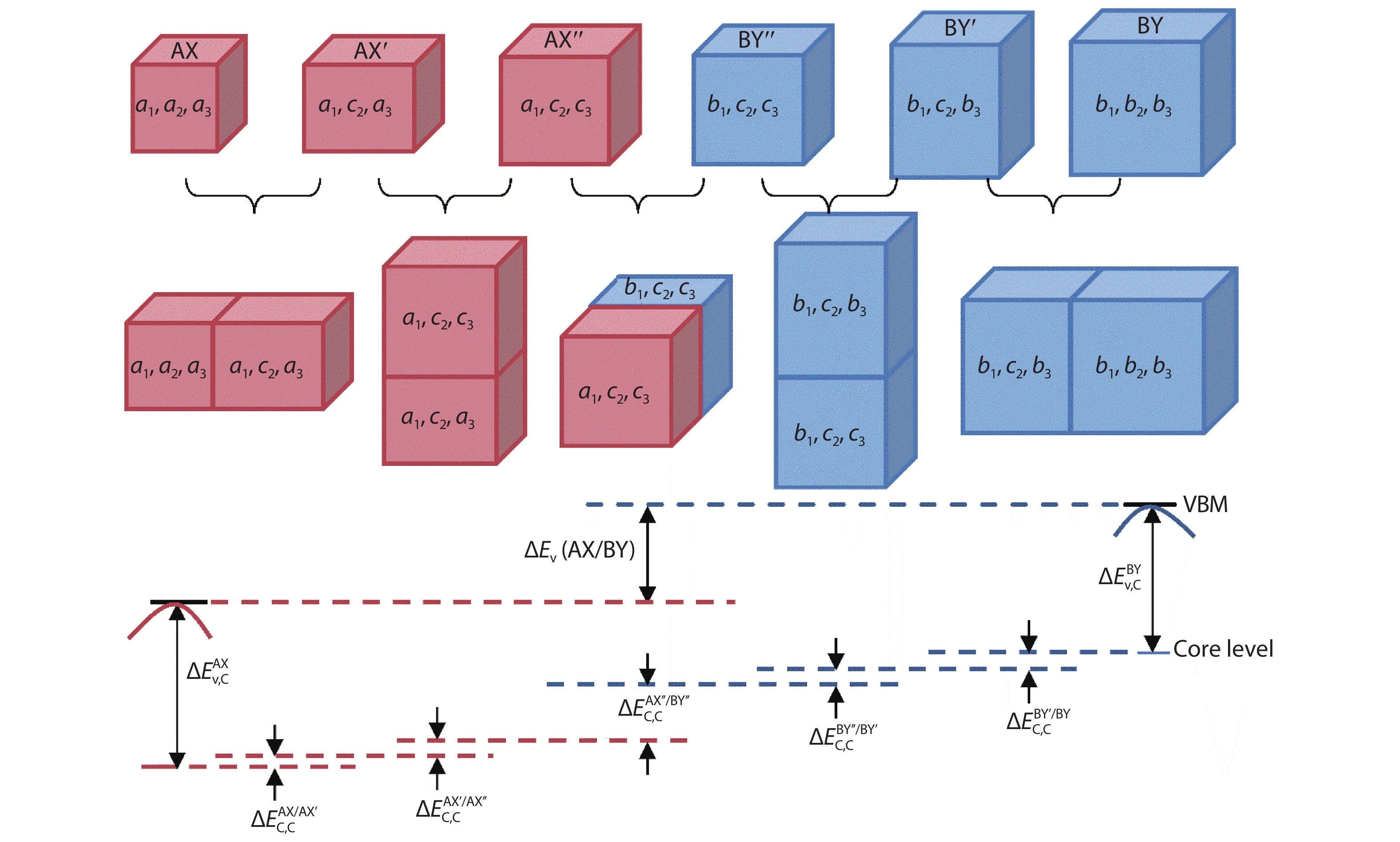
Fig. 1.
(Color online) Five steps for correcting the effect of lattice mismatch on valence band offset calculations using core energy levels as a reference.
ARTICLES
Yuying Hu1, 2, Chen Qiu1, Tao Shen1, 2, Kaike Yang3 and Huixiong Deng1, 2,
Corresponding author: Huixiong Deng, hxdeng@semi.ac.cn
Abstract: Band offset in semiconductors is a fundamental physical quantity that determines the performance of optoelectronic devices. However, the current method of calculating band offset is difficult to apply directly to the large-lattice-mismatched and heterovalent semiconductors because of the existing electric field and large strain at the interfaces. Here, we proposed a modified method to calculate band offsets for such systems, in which the core energy level shifts caused by heterovalent effects and lattice mismatch are estimated by interface reconstruction and the insertion of unidirectional strain structures as transitions, respectively. Taking the Si and III–V systems as examples, the results have the same accuracy as what is a widely used method for small-lattice-mismatched systems, and are much closer to the experimental values for the large-lattice-mismatched and heterovalent systems. Furthermore, by systematically studying the heterojunctions of Si and III–V semiconductors along different directions, it is found that the band offsets of Si/InAs and Si/InSb systems in [100], [110] and [111] directions belong to the type I, and could be beneficial for silicon-based luminescence performance. Our study offers a more reliable and direct method for calculating band offsets of large-lattice-mismatched and heterovalent semiconductors, and could provide theoretical support for the design of the high-performance silicon-based light sources.
Keywords: Si-based luminescence, band offset, lattice mismatch, heterovalent semiconductors
| [1] |
Bioud Y A, Boucherif A, Myronov M, et al. Uprooting defects to enable high-performance III–V optoelectronic devices on silicon. Nat Commun, 2019, 10, 4322 doi: 10.1038/s41467-019-12353-9
|
| [2] |
Zacharias M, Kelires P C. Temperature dependence of the optical properties of silicon nanocrystals. Phys Rev B, 2020, 101(24), 245122 doi: 10.1103/PhysRevB.101.245122
|
| [3] |
Lu P, Li D, Cao Y, et al. Si nanocrystals-based multilayers for luminescent and photovoltaic device applications. J Semicond, 2018, 39(6), 061007 doi: 10.1088/1674-4926/39/6/061007
|
| [4] |
Zhao S, Liu X, Pi X, et al. Light-emitting diodes based on colloidal silicon quantum dots. J Semicond, 2018, 39(6), 061008 doi: 10.1088/1674-4926/39/6/061008
|
| [5] |
Zheng J, Liu Z, Xue C, et al. Recent progress in GeSn growth and GeSn-based photonic devices. J Semicond, 2018, 39(6), 061006 doi: 10.1088/1674-4926/39/6/061006
|
| [6] |
Boras G, Yu X, Liu H. III–V ternary nanowires on Si substrates: growth, characterization and device applications. J Semicond, 2019, 40(10), 101301 doi: 10.1088/1674-4926/40/10/101301
|
| [7] |
Zhang J, Yang X, Feng Y, et al. Vacancy-engineering-induced dislocation inclination in III-nitrides on Si substrates. Phys Rev Mater, 2020, 4(7), 073402 doi: 10.1103/PhysRevMaterials.4.073402
|
| [8] |
Zhao C, Xu B, Wang Z, et al. Boron-doped III–V semiconductors for Si-based optoelectronic devices. J Semicond, 2020, 41(1), 011301 doi: 10.1088/1674-4926/41/1/011301
|
| [9] |
Chen S, Li W, Wu J, et al. Electrically pumped continuous-wave III–V quantum dot lasers on silicon. Nat Photonics, 2016, 10(5), 307 doi: 10.1038/nphoton.2016.21
|
| [10] |
Shang C, Gossard A C, Bowers J E, et al. Low-threshold epitaxially grown 1.3-μm InAs quantum dot lasers on patterned (001) Si. IEEE J Sel Top Quantum Electron, 2019, 25(6), 1502207 doi: 10.1109/JSTQE.2019.2927581
|
| [11] |
Van de Walle C G. Band lineups and deformation potentials in the model-solid theory. Phys Rev B, 1989, 39(3), 1871 doi: 10.1103/PhysRevB.39.1871
|
| [12] |
Deng H X, Luo J W, Wei S H. Chemical trends of stability and band alignment of lattice-matched II–VI/III–V semiconductor interfaces. Phys Rev B, 2015, 91(7), 075315 doi: 10.1103/PhysRevB.91.075315
|
| [13] |
Mano T, Fujioka H, Ono K, et al. InAs nanocrystal growth on Si (100). Appl Surf Sci, 1998, 130, 760 doi: 10.1016/S0169-4332(98)00150-0
|
| [14] |
Heitz R, Ledentsov N N, Bimberg D, et al. Optical properties of InAs quantum dots in a Si matrix. Appl Phys Lett, 1999, 74(12), 1701 doi: 10.1063/1.123660
|
| [15] |
Tersoff J. Theory of semiconductor heterojunctions: The role of quantum dipoles. Phys Rev B, 1984, 30(8), 4874 doi: 10.1103/PhysRevB.30.4874
|
| [16] |
Bru-Chevallier C, El Akra A, Pelloux-Gervais D, et al. InGaAs quantum dots grown by molecular beam epitaxy for light emission on Si substrates. J Nanosci Nanotechnol, 2011, 11(10), 9153 doi: 10.1166/jnn.2011.4282
|
| [17] |
Li Y H, Walsh A, Chen S, et al. Revised ab initio natural band offsets of all group IV, II–VI, and III–V semiconductors. Appl Phys Lett, 2009, 94(21), 212109 doi: 10.1063/1.3143626
|
| [18] |
Lang L, Zhang Y Y, Xu P, et al. Three-step approach for computing band offsets and its application to inorganic ABX3 halide perovskites. Phys Rev B, 2015, 92(7), 075102 doi: 10.1103/PhysRevB.92.075102
|
| [19] |
Hohenberg P, Kohn W. Inhomogeneous electron gas. Phys Rev, 1964, 136(3B), B864 doi: 10.1103/PhysRev.136.B864
|
| [20] |
Kohn W, Sham L J. Self-consistent equations including exchange and correlation effects. Phys Rev, 1965, 140(4A), A1133 doi: 10.1103/PhysRev.140.A1133
|
| [21] |
Ceperley D M, Alder B J. Ground state of the electron Gas by a stochastic method. Phys Rev Lett, 1980, 45(7), 566 doi: 10.1103/PhysRevLett.45.566
|
| [22] |
Kresse G, Furthmüller J. Efficiency of ab-initio total energy calculations for metals and semiconductors using a plane-wave basis set. Phys Rev Lett, 1996, 6(1), 15 doi: 10.1016/0927-0256(96)00008-0
|
| [23] |
Madelung O. Semiconductors: data handbook. Springer Science & Business Media, 2004
|
| [24] |
Wei S H, Zunger A. Calculated natural band offsets of all II–VI and III–V semiconductors: Chemical trends and the role of cation d orbitals. Appl Phys Lett, 1998, 72(16), 2011 doi: 10.1063/1.121249
|
| [25] |
Deng H X, Huang B, Wei S H. Stable interface structures of heterovalent semiconductor superlattices: The case of (GaSb)n(ZnTe)n. Comput Mater Sci, 2015, 98, 340 doi: 10.1016/j.commatsci.2014.11.008
|
| [26] |
Christensen N E. Dipole effects and band offsets at semiconductor interfaces. Phys Rev B, 1988, 37(9), 4528 doi: 10.1103/PhysRevB.37.4528
|
| [27] |
Saive R, Emmer H, Chen C T, et al. Study of the interface in a GaP/Si heterojunction solar cell. IEEE J Photovolt, 2018, 8, 1568 doi: 10.1109/JPHOTOV.2018.2861724
|
| [28] |
Han C B, He C, Li X J. Near-infrared light emission from a GaN/Si nanoheterostructure array. Adv Mater, 2011, 23(41), 4811 doi: 10.1002/adma.201101801
|
| [29] |
List R S, Woicik J C, Lindau I, et al. The Si/GaAs (110) heterojunction: Strain, disorder, and valence-band discontinuity. J Vac Sci Technol B, 1987, 5(4), 1279 doi: 10.1116/1.583819
|
| [30] |
Van de Walle C G, Martin R M. Theoretical calculations of heterojunction discontinuities in the Si/Ge system. Phys Rev B, 1986, 34(8), 5621 doi: 10.1103/PhysRevB.34.5621
|
| [31] |
Pollard W. Valence-band discontinuities at semiconductor heterojunctions. J Appl Phys, 1991, 69(5), 3154 doi: 10.1063/1.348584
|
| [32] |
Halder N N, Biswas P, Nagabhushan B, et al. Effect of band offset on carrier transport and infrared detection in InP quantum dots/Si nano-heterojunction grown by metalorganic chemical vapor deposition technique. J Appl Phys, 2014, 115(20), 203719 doi: 10.1063/1.4880738
|
| [33] |
Katnani A D, Margaritondo G. Microscopic study of semiconductor heterojunctions: Photoemission measurement of the valance-band discontinuity and of the potential barriers. Phys Rev B, 1983, 28(4), 1944 doi: 10.1103/PhysRevB.28.1944
|
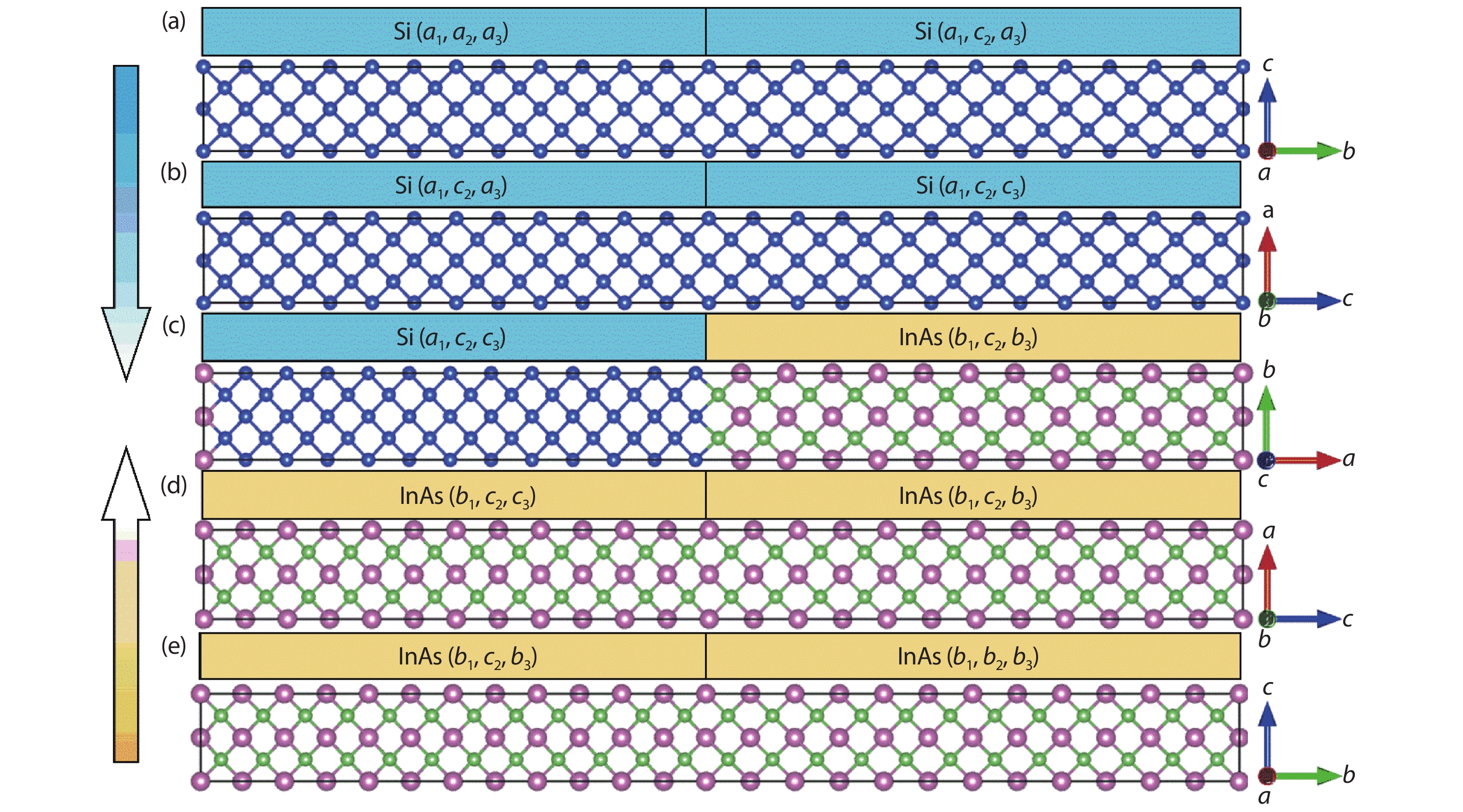
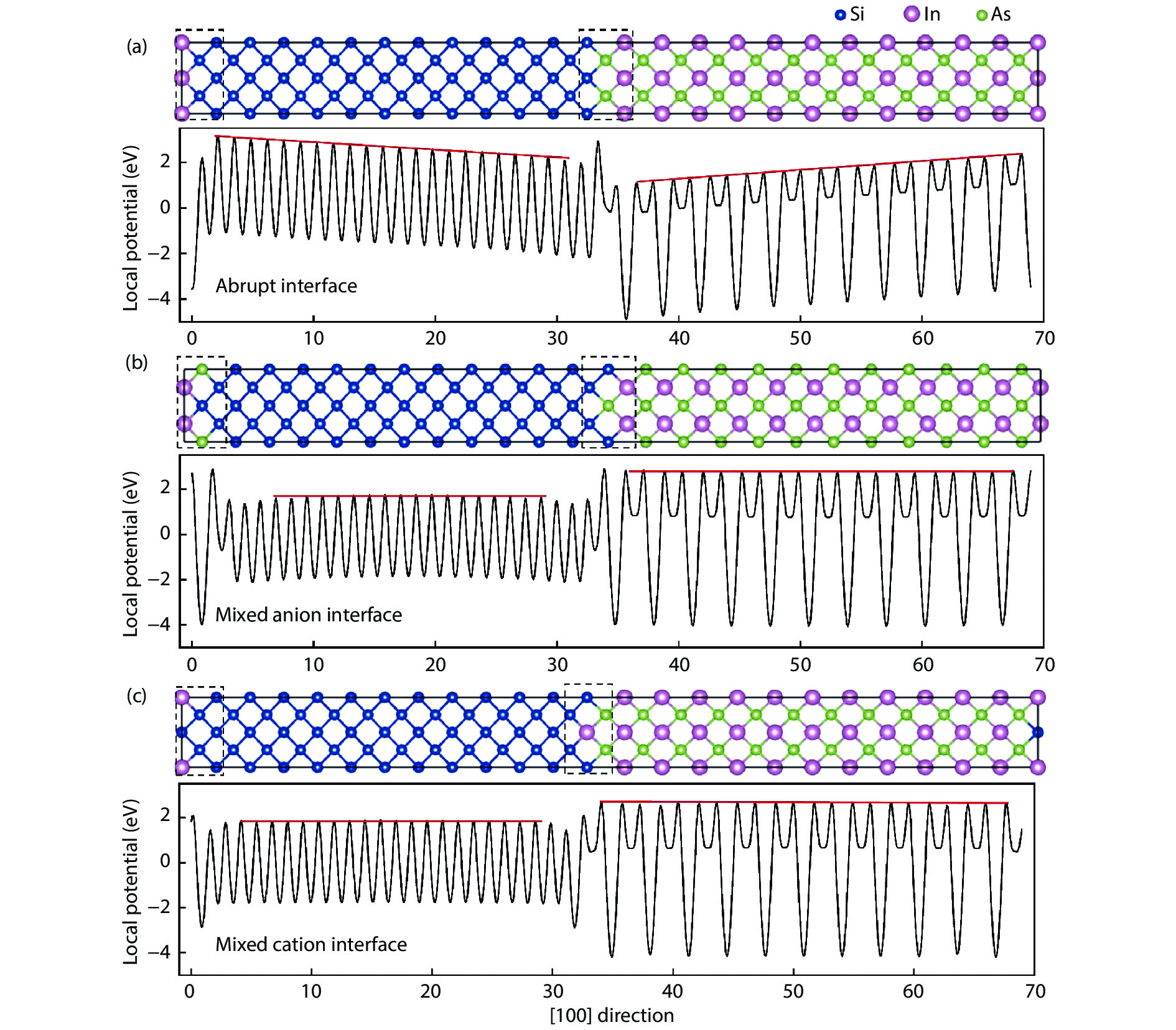

Table 1. Valence band offsets (in eV) of Si/III–V semiconductors with lattice mismatch and heterovalence along the orientation of [100], [110], [111], respectively. The lattice constants (in Å) of III–V semiconductors and mismatches (referred to the lattice constant of Si, e.g. 5.43 Å) are also given. The positive value represents that the position of the valence band of the III–V semiconductor is higher than that of Si.
| System | Lattice constant | Mismatch (%) | [100] | [110] abrupt | [111] | Exp.\Theo. | ||||
| Mixed anion | Mixed cation | Average | Mixed anion | Mixed cation | Average | |||||
| Si/AlP | 5.46 | 0.55 | –0.56 | –1.21 | –0.88 | –0.84 | –0.59 | –1.22 | –0.91 | –\–0.91i |
| Si/AlAs | 5.66 | 4.24 | –0.07 | –0.70 | –0.39 | –0.26 | 0.05 | –0.53 | –0.24 | –\– |
| Si/AlSb | 6.14 | 13.08 | 0.31 | 0.26 | 0.28 | 0.52 | 0.37 | 0.41 | 0.39 | –\– |
| Si/GaN | 4.53 | –16.57 | –1.92 | –1.99 | –1.95 | –2.00 | –1.52 | –1.68 | –1.60 | –1.90ii\– |
| Si/GaP | 5.45 | 0.37 | 0.04 | –0.59 | –0.28 | –0.28 | 0.02 | –0.58 | –0.28 | –0.24±0.12iii \–0.27i |
| Si/GaAs | 5.65 | 4.05 | 0.29 | –0.09 | 0.10 | 0.28 | 0.51 | 0.11 | 0.31 | 0.23±0.10iv \0.12v |
| Si/GaSb | 6.10 | 12.34 | 0.41 | 0.26 | 0.34 | 0.62 | 0.36 | 0.27 | 0.31 | –\– |
| Si/InP | 5.87 | 8.10 | 0.10 | –0.27 | –0.08 | 0.25 | 0.43 | 0.07 | 0.25 | 0.12vi\0.36vii |
| Si/InAs | 6.06 | 11.60 | 0.29 | 0.11 | 0.20 | 0.42 | 0.42 | 0.37 | 0.40 | 0.31viii\0.50vii |
| Si/InSb | 6.48 | 19.34 | 0.16 | 0.14 | 0.15 | 0.73 | 0.22 | 0.24 | 0.23 | 0.06ix\0.25vii |
| i from Ref. [26]; ii from Ref. [28]; iii from Ref. [27]; iv from Ref. [29]; v from Ref. [30]; vi from Ref. [32]; vii from Ref. [31]; Viii from Ref. [13]; ix from Ref. [33]. | ||||||||||
 DownLoad: CSV
| [1] |
Bioud Y A, Boucherif A, Myronov M, et al. Uprooting defects to enable high-performance III–V optoelectronic devices on silicon. Nat Commun, 2019, 10, 4322 doi: 10.1038/s41467-019-12353-9
|
| [2] |
Zacharias M, Kelires P C. Temperature dependence of the optical properties of silicon nanocrystals. Phys Rev B, 2020, 101(24), 245122 doi: 10.1103/PhysRevB.101.245122
|
| [3] |
Lu P, Li D, Cao Y, et al. Si nanocrystals-based multilayers for luminescent and photovoltaic device applications. J Semicond, 2018, 39(6), 061007 doi: 10.1088/1674-4926/39/6/061007
|
| [4] |
Zhao S, Liu X, Pi X, et al. Light-emitting diodes based on colloidal silicon quantum dots. J Semicond, 2018, 39(6), 061008 doi: 10.1088/1674-4926/39/6/061008
|
| [5] |
Zheng J, Liu Z, Xue C, et al. Recent progress in GeSn growth and GeSn-based photonic devices. J Semicond, 2018, 39(6), 061006 doi: 10.1088/1674-4926/39/6/061006
|
| [6] |
Boras G, Yu X, Liu H. III–V ternary nanowires on Si substrates: growth, characterization and device applications. J Semicond, 2019, 40(10), 101301 doi: 10.1088/1674-4926/40/10/101301
|
| [7] |
Zhang J, Yang X, Feng Y, et al. Vacancy-engineering-induced dislocation inclination in III-nitrides on Si substrates. Phys Rev Mater, 2020, 4(7), 073402 doi: 10.1103/PhysRevMaterials.4.073402
|
| [8] |
Zhao C, Xu B, Wang Z, et al. Boron-doped III–V semiconductors for Si-based optoelectronic devices. J Semicond, 2020, 41(1), 011301 doi: 10.1088/1674-4926/41/1/011301
|
| [9] |
Chen S, Li W, Wu J, et al. Electrically pumped continuous-wave III–V quantum dot lasers on silicon. Nat Photonics, 2016, 10(5), 307 doi: 10.1038/nphoton.2016.21
|
| [10] |
Shang C, Gossard A C, Bowers J E, et al. Low-threshold epitaxially grown 1.3-μm InAs quantum dot lasers on patterned (001) Si. IEEE J Sel Top Quantum Electron, 2019, 25(6), 1502207 doi: 10.1109/JSTQE.2019.2927581
|
| [11] |
Van de Walle C G. Band lineups and deformation potentials in the model-solid theory. Phys Rev B, 1989, 39(3), 1871 doi: 10.1103/PhysRevB.39.1871
|
| [12] |
Deng H X, Luo J W, Wei S H. Chemical trends of stability and band alignment of lattice-matched II–VI/III–V semiconductor interfaces. Phys Rev B, 2015, 91(7), 075315 doi: 10.1103/PhysRevB.91.075315
|
| [13] |
Mano T, Fujioka H, Ono K, et al. InAs nanocrystal growth on Si (100). Appl Surf Sci, 1998, 130, 760 doi: 10.1016/S0169-4332(98)00150-0
|
| [14] |
Heitz R, Ledentsov N N, Bimberg D, et al. Optical properties of InAs quantum dots in a Si matrix. Appl Phys Lett, 1999, 74(12), 1701 doi: 10.1063/1.123660
|
| [15] |
Tersoff J. Theory of semiconductor heterojunctions: The role of quantum dipoles. Phys Rev B, 1984, 30(8), 4874 doi: 10.1103/PhysRevB.30.4874
|
| [16] |
Bru-Chevallier C, El Akra A, Pelloux-Gervais D, et al. InGaAs quantum dots grown by molecular beam epitaxy for light emission on Si substrates. J Nanosci Nanotechnol, 2011, 11(10), 9153 doi: 10.1166/jnn.2011.4282
|
| [17] |
Li Y H, Walsh A, Chen S, et al. Revised ab initio natural band offsets of all group IV, II–VI, and III–V semiconductors. Appl Phys Lett, 2009, 94(21), 212109 doi: 10.1063/1.3143626
|
| [18] |
Lang L, Zhang Y Y, Xu P, et al. Three-step approach for computing band offsets and its application to inorganic ABX3 halide perovskites. Phys Rev B, 2015, 92(7), 075102 doi: 10.1103/PhysRevB.92.075102
|
| [19] |
Hohenberg P, Kohn W. Inhomogeneous electron gas. Phys Rev, 1964, 136(3B), B864 doi: 10.1103/PhysRev.136.B864
|
| [20] |
Kohn W, Sham L J. Self-consistent equations including exchange and correlation effects. Phys Rev, 1965, 140(4A), A1133 doi: 10.1103/PhysRev.140.A1133
|
| [21] |
Ceperley D M, Alder B J. Ground state of the electron Gas by a stochastic method. Phys Rev Lett, 1980, 45(7), 566 doi: 10.1103/PhysRevLett.45.566
|
| [22] |
Kresse G, Furthmüller J. Efficiency of ab-initio total energy calculations for metals and semiconductors using a plane-wave basis set. Phys Rev Lett, 1996, 6(1), 15 doi: 10.1016/0927-0256(96)00008-0
|
| [23] |
Madelung O. Semiconductors: data handbook. Springer Science & Business Media, 2004
|
| [24] |
Wei S H, Zunger A. Calculated natural band offsets of all II–VI and III–V semiconductors: Chemical trends and the role of cation d orbitals. Appl Phys Lett, 1998, 72(16), 2011 doi: 10.1063/1.121249
|
| [25] |
Deng H X, Huang B, Wei S H. Stable interface structures of heterovalent semiconductor superlattices: The case of (GaSb)n(ZnTe)n. Comput Mater Sci, 2015, 98, 340 doi: 10.1016/j.commatsci.2014.11.008
|
| [26] |
Christensen N E. Dipole effects and band offsets at semiconductor interfaces. Phys Rev B, 1988, 37(9), 4528 doi: 10.1103/PhysRevB.37.4528
|
| [27] |
Saive R, Emmer H, Chen C T, et al. Study of the interface in a GaP/Si heterojunction solar cell. IEEE J Photovolt, 2018, 8, 1568 doi: 10.1109/JPHOTOV.2018.2861724
|
| [28] |
Han C B, He C, Li X J. Near-infrared light emission from a GaN/Si nanoheterostructure array. Adv Mater, 2011, 23(41), 4811 doi: 10.1002/adma.201101801
|
| [29] |
List R S, Woicik J C, Lindau I, et al. The Si/GaAs (110) heterojunction: Strain, disorder, and valence-band discontinuity. J Vac Sci Technol B, 1987, 5(4), 1279 doi: 10.1116/1.583819
|
| [30] |
Van de Walle C G, Martin R M. Theoretical calculations of heterojunction discontinuities in the Si/Ge system. Phys Rev B, 1986, 34(8), 5621 doi: 10.1103/PhysRevB.34.5621
|
| [31] |
Pollard W. Valence-band discontinuities at semiconductor heterojunctions. J Appl Phys, 1991, 69(5), 3154 doi: 10.1063/1.348584
|
| [32] |
Halder N N, Biswas P, Nagabhushan B, et al. Effect of band offset on carrier transport and infrared detection in InP quantum dots/Si nano-heterojunction grown by metalorganic chemical vapor deposition technique. J Appl Phys, 2014, 115(20), 203719 doi: 10.1063/1.4880738
|
| [33] |
Katnani A D, Margaritondo G. Microscopic study of semiconductor heterojunctions: Photoemission measurement of the valance-band discontinuity and of the potential barriers. Phys Rev B, 1983, 28(4), 1944 doi: 10.1103/PhysRevB.28.1944
|


Article views: 5144 Times PDF downloads: 193 Times Cited by: 0 Times
Received: 30 April 2021 Revised: Online: Accepted Manuscript: 11 June 2021Uncorrected proof: 21 June 2021Published: 01 November 2021
| Citation: |
Yuying Hu, Chen Qiu, Tao Shen, Kaike Yang, Huixiong Deng. Direct calculations on the band offsets of large-lattice-mismatched and heterovalent Si and III–V semiconductors[J]. Journal of Semiconductors, 2021, 42(11): 112102. doi: 10.1088/1674-4926/42/11/112102
****
Y Y Hu, C Qiu, T Shen, K K Yang, H X Deng, Direct calculations on the band offsets of large-lattice-mismatched and heterovalent Si and III–V semiconductors[J]. J. Semicond., 2021, 42(11): 112102. doi: 10.1088/1674-4926/42/11/112102.

|
| [1] |
Bioud Y A, Boucherif A, Myronov M, et al. Uprooting defects to enable high-performance III–V optoelectronic devices on silicon. Nat Commun, 2019, 10, 4322 doi: 10.1038/s41467-019-12353-9
|
| [2] |
Zacharias M, Kelires P C. Temperature dependence of the optical properties of silicon nanocrystals. Phys Rev B, 2020, 101(24), 245122 doi: 10.1103/PhysRevB.101.245122
|
| [3] |
Lu P, Li D, Cao Y, et al. Si nanocrystals-based multilayers for luminescent and photovoltaic device applications. J Semicond, 2018, 39(6), 061007 doi: 10.1088/1674-4926/39/6/061007
|
| [4] |
Zhao S, Liu X, Pi X, et al. Light-emitting diodes based on colloidal silicon quantum dots. J Semicond, 2018, 39(6), 061008 doi: 10.1088/1674-4926/39/6/061008
|
| [5] |
Zheng J, Liu Z, Xue C, et al. Recent progress in GeSn growth and GeSn-based photonic devices. J Semicond, 2018, 39(6), 061006 doi: 10.1088/1674-4926/39/6/061006
|
| [6] |
Boras G, Yu X, Liu H. III–V ternary nanowires on Si substrates: growth, characterization and device applications. J Semicond, 2019, 40(10), 101301 doi: 10.1088/1674-4926/40/10/101301
|
| [7] |
Zhang J, Yang X, Feng Y, et al. Vacancy-engineering-induced dislocation inclination in III-nitrides on Si substrates. Phys Rev Mater, 2020, 4(7), 073402 doi: 10.1103/PhysRevMaterials.4.073402
|
| [8] |
Zhao C, Xu B, Wang Z, et al. Boron-doped III–V semiconductors for Si-based optoelectronic devices. J Semicond, 2020, 41(1), 011301 doi: 10.1088/1674-4926/41/1/011301
|
| [9] |
Chen S, Li W, Wu J, et al. Electrically pumped continuous-wave III–V quantum dot lasers on silicon. Nat Photonics, 2016, 10(5), 307 doi: 10.1038/nphoton.2016.21
|
| [10] |
Shang C, Gossard A C, Bowers J E, et al. Low-threshold epitaxially grown 1.3-μm InAs quantum dot lasers on patterned (001) Si. IEEE J Sel Top Quantum Electron, 2019, 25(6), 1502207 doi: 10.1109/JSTQE.2019.2927581
|
| [11] |
Van de Walle C G. Band lineups and deformation potentials in the model-solid theory. Phys Rev B, 1989, 39(3), 1871 doi: 10.1103/PhysRevB.39.1871
|
| [12] |
Deng H X, Luo J W, Wei S H. Chemical trends of stability and band alignment of lattice-matched II–VI/III–V semiconductor interfaces. Phys Rev B, 2015, 91(7), 075315 doi: 10.1103/PhysRevB.91.075315
|
| [13] |
Mano T, Fujioka H, Ono K, et al. InAs nanocrystal growth on Si (100). Appl Surf Sci, 1998, 130, 760 doi: 10.1016/S0169-4332(98)00150-0
|
| [14] |
Heitz R, Ledentsov N N, Bimberg D, et al. Optical properties of InAs quantum dots in a Si matrix. Appl Phys Lett, 1999, 74(12), 1701 doi: 10.1063/1.123660
|
| [15] |
Tersoff J. Theory of semiconductor heterojunctions: The role of quantum dipoles. Phys Rev B, 1984, 30(8), 4874 doi: 10.1103/PhysRevB.30.4874
|
| [16] |
Bru-Chevallier C, El Akra A, Pelloux-Gervais D, et al. InGaAs quantum dots grown by molecular beam epitaxy for light emission on Si substrates. J Nanosci Nanotechnol, 2011, 11(10), 9153 doi: 10.1166/jnn.2011.4282
|
| [17] |
Li Y H, Walsh A, Chen S, et al. Revised ab initio natural band offsets of all group IV, II–VI, and III–V semiconductors. Appl Phys Lett, 2009, 94(21), 212109 doi: 10.1063/1.3143626
|
| [18] |
Lang L, Zhang Y Y, Xu P, et al. Three-step approach for computing band offsets and its application to inorganic ABX3 halide perovskites. Phys Rev B, 2015, 92(7), 075102 doi: 10.1103/PhysRevB.92.075102
|
| [19] |
Hohenberg P, Kohn W. Inhomogeneous electron gas. Phys Rev, 1964, 136(3B), B864 doi: 10.1103/PhysRev.136.B864
|
| [20] |
Kohn W, Sham L J. Self-consistent equations including exchange and correlation effects. Phys Rev, 1965, 140(4A), A1133 doi: 10.1103/PhysRev.140.A1133
|
| [21] |
Ceperley D M, Alder B J. Ground state of the electron Gas by a stochastic method. Phys Rev Lett, 1980, 45(7), 566 doi: 10.1103/PhysRevLett.45.566
|
| [22] |
Kresse G, Furthmüller J. Efficiency of ab-initio total energy calculations for metals and semiconductors using a plane-wave basis set. Phys Rev Lett, 1996, 6(1), 15 doi: 10.1016/0927-0256(96)00008-0
|
| [23] |
Madelung O. Semiconductors: data handbook. Springer Science & Business Media, 2004
|
| [24] |
Wei S H, Zunger A. Calculated natural band offsets of all II–VI and III–V semiconductors: Chemical trends and the role of cation d orbitals. Appl Phys Lett, 1998, 72(16), 2011 doi: 10.1063/1.121249
|
| [25] |
Deng H X, Huang B, Wei S H. Stable interface structures of heterovalent semiconductor superlattices: The case of (GaSb)n(ZnTe)n. Comput Mater Sci, 2015, 98, 340 doi: 10.1016/j.commatsci.2014.11.008
|
| [26] |
Christensen N E. Dipole effects and band offsets at semiconductor interfaces. Phys Rev B, 1988, 37(9), 4528 doi: 10.1103/PhysRevB.37.4528
|
| [27] |
Saive R, Emmer H, Chen C T, et al. Study of the interface in a GaP/Si heterojunction solar cell. IEEE J Photovolt, 2018, 8, 1568 doi: 10.1109/JPHOTOV.2018.2861724
|
| [28] |
Han C B, He C, Li X J. Near-infrared light emission from a GaN/Si nanoheterostructure array. Adv Mater, 2011, 23(41), 4811 doi: 10.1002/adma.201101801
|
| [29] |
List R S, Woicik J C, Lindau I, et al. The Si/GaAs (110) heterojunction: Strain, disorder, and valence-band discontinuity. J Vac Sci Technol B, 1987, 5(4), 1279 doi: 10.1116/1.583819
|
| [30] |
Van de Walle C G, Martin R M. Theoretical calculations of heterojunction discontinuities in the Si/Ge system. Phys Rev B, 1986, 34(8), 5621 doi: 10.1103/PhysRevB.34.5621
|
| [31] |
Pollard W. Valence-band discontinuities at semiconductor heterojunctions. J Appl Phys, 1991, 69(5), 3154 doi: 10.1063/1.348584
|
| [32] |
Halder N N, Biswas P, Nagabhushan B, et al. Effect of band offset on carrier transport and infrared detection in InP quantum dots/Si nano-heterojunction grown by metalorganic chemical vapor deposition technique. J Appl Phys, 2014, 115(20), 203719 doi: 10.1063/1.4880738
|
| [33] |
Katnani A D, Margaritondo G. Microscopic study of semiconductor heterojunctions: Photoemission measurement of the valance-band discontinuity and of the potential barriers. Phys Rev B, 1983, 28(4), 1944 doi: 10.1103/PhysRevB.28.1944
|

 WeChat ID
Journal of Semiconductors © 2017 All Rights Reserved 京ICP备05085259号-2


