


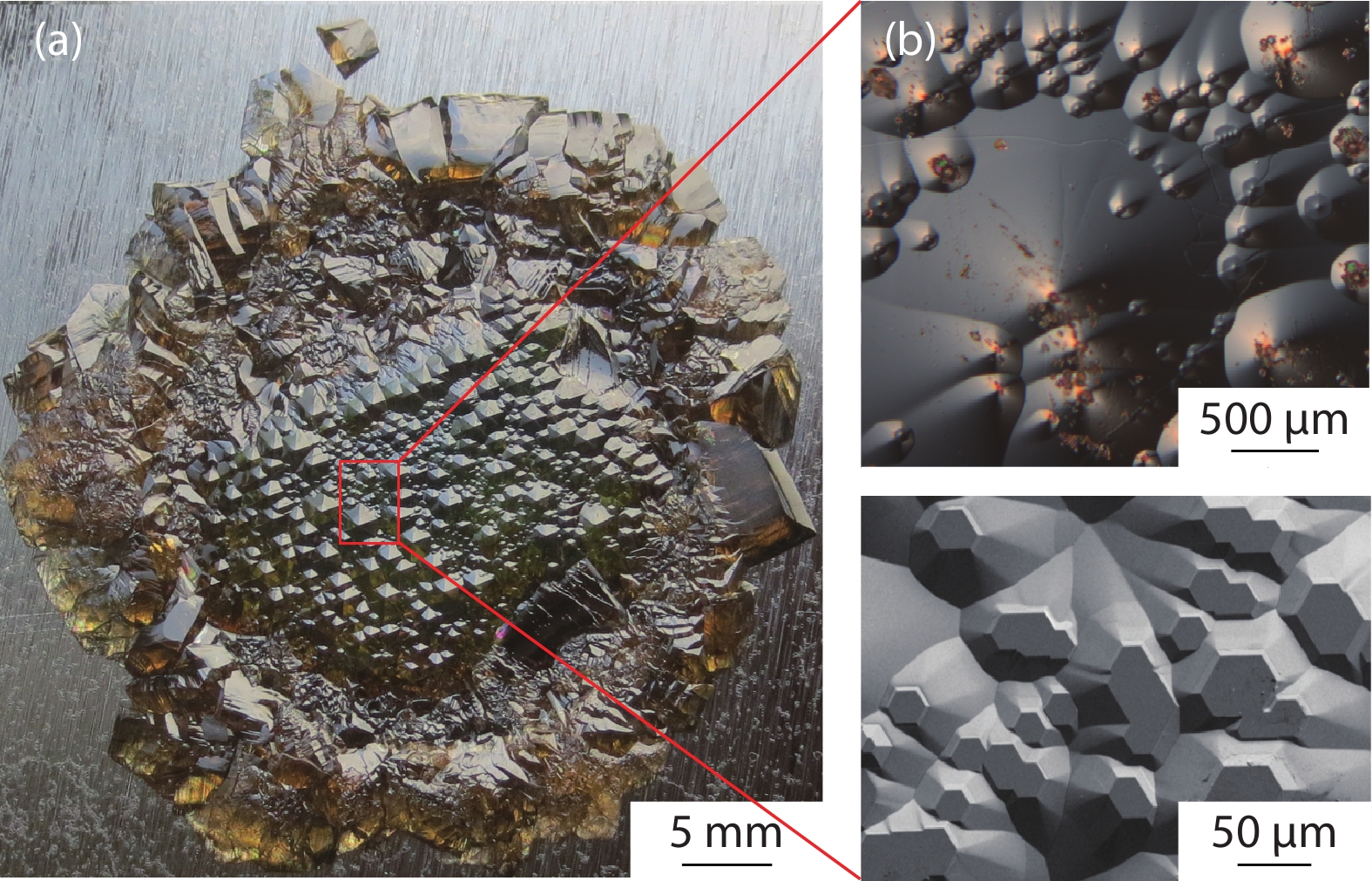
Fig. 1.
(Color online) Surface topography of the AlN crystal grown at a seed surface temperature of 2200 °C. (a) Photograph. (b) Differential interference microscope. (c) SEM image.
ARTICLES
Li Zhang1, Haitao Qi1, , Hongjuan Cheng1, Yuezeng Shi1, Zhanpin Lai1 and Muchang Luo2
Corresponding author: Haitao Qi, Email: tjuqht1@163.com
Abstract: AlN single crystal grown by physical vapor transport (PVT) using homogeneous seed is considered as the most promising approach to obtain high-quality AlN boule. In this work, the morphology of AlN single crystals grown under different modes (3D islands and single spiral center) were investigated. It is proved that, within an optimized thermal distribution chamber system, the surface temperature of AlN seed plays an important role in crystal growth, revealing a direct relationship between growth mode and growth condition. Notably, a high-quality AlN crystal, with (002) and (102) reflection peaks of 65 and 36 arcsec at full width at half maximum (FWHM), was obtained grown under a single spiral center mode. And on which, a high-quality AlxGa1–xN epitaxial layer with high Al content (x = 0.54) was also obtained. The FWHMs of (002) and (102) reflection of AlxGa1–xN were 202 and 496 arcsec, respectively, which shows superiority over their counterpart grown on SiC or a sapphire substrate.
Keywords: AlN crystal, surface morphology, growth mechanism, crystalline quality
| [1] |
Hartmann C, Dittmar A, Wollweber J, et al. Bulk AlN growth by physical vapour transport. Semicond Sci Technol, 2014, 29, 084002 doi: 10.1088/0268-1242/29/8/084002
|
| [2] |
Filip O, Epelbaum B M, Bickermann M, et al. Effects of growth direction and polarity on bulk aluminum nitride crystal properties. J Cryst Growth, 2011, 318, 427 doi: 10.1016/j.jcrysgro.2010.10.198
|
| [3] |
Slack G A, McNelly T F. Growth of high purity AlN crystals. J Cryst Growth, 1976, 34, 263 doi: 10.1016/0022-0248(76)90139-1
|
| [4] |
Mokhov E, Izmaylova I, Kazarova O, et al. Specific features of sublimation growth of bulk AlN crystals on SiC wafers. Phys Status Solidi C, 2013, 10, 445 doi: 10.1002/pssc.201200638
|
| [5] |
Bickermann M, Filip O, Epelbaum B M, et al. Growth of AlN bulk crystals on SiC seeds: Chemical analysis and crystal properties. J Cryst Growth, 2012, 339, 13 doi: 10.1016/j.jcrysgro.2011.11.043
|
| [6] |
Nagai I, Kato T, Miura T, et al. AlN bulk single crystal growth on 6H-SiC substrates by sublimation method. J Cryst Growth, 2010, 312, 2699 doi: 10.1016/j.jcrysgro.2010.05.044
|
| [7] |
Hartmann C, Albrecht M, Wollweber J, et al. SiC seed polarity-dependent bulk AlN growth under the influence of residual oxygen. J Cryst Growth, 2012, 344, 19 doi: 10.1016/j.jcrysgro.2012.01.045
|
| [8] |
Chemekova T Y, Avdeev O V, Barash I S, et al. Sublimation growth of 2 inch diameter bulk AlN crystals. Phys Status Solidi C, 2008, 5, 1612 doi: 10.1002/pssc.200778534
|
| [9] |
Bickermann M, Epelbaum B M, Filip O, et al. Faceting in AlN bulk crystal growth and its impact on optical properties of the crystals. Phys Status Solidi C, 2012, 9, 449 doi: 10.1002/pssc.201100345
|
| [10] |
Sumathi R R, Barz R U, Straubinger T, et al. Structural and surface topography analysis of AlN single crystals grown on 6H-SiC substrates. J Cryst Growth, 2012, 360, 193 doi: 10.1016/j.jcrysgro.2011.11.054
|
| [11] |
Dalmau R, Craft H S, Britt J, et al. High quality AlN single crystal substrates for AlGaN-based devices. Mater Sci Forum, 2018, 924, 923 doi: 10.4028/www.scientific.net/MSF.924.923
|
| [12] |
Hartmann C, Matiwe L, Wollweber J, et al. Favourable growth conditions for the preparation of bulk AlN single crystals by PVT. CrystEngComm, 2020, 22, 1762 doi: 10.1039/C9CE01952A
|
| [13] |
Sumathi R R. Bulk AlN single crystal growth on foreign substrate and preparation of free-standing native seeds. CrystEngComm, 2013, 15, 2232 doi: 10.1039/C2CE26599K
|
| [14] |
Zhang L, Qi H T, Cheng H J, et al. Preparation and characterization of AlN seeds for homogeneous growth. J Semicond, 2019, 40, 102801 doi: 10.1088/40/10/102801
|
| [15] |
Bickermann M, Epelbaum B M, Filip O, et al. Deep-UV transparent bulk single-crystalline AlN substrates. Phys Status Solidi C, 2010, 7, 1743 doi: 10.1002/pssc.200983422
|
| [16] |
Bickermann M, Epelbaum B M, Filip O, et al. UV transparent single-crystalline bulk AlN substrates. Phys Status Solidi C, 2010, 7, 21 doi: 10.1002/pssc.200982601
|
| [17] |
Yang W X, Zhao Y K, Wu Y Y, et al. Deep-UV emission at 260 nm from MBE-grown AlGaN/AlN quantum-well structures. J Cryst Growth, 2019, 512, 213 doi: 10.1016/j.jcrysgro.2019.02.037
|
| [18] |
Bobea Graziano M, Bryan I, Bryan Z, et al. Structural characteristics of m-plane AlN substrates and homoepitaxial films. J Cryst Growth, 2019, 507, 389 doi: 10.1016/j.jcrysgro.2018.07.012
|
| [19] |
Zheng W, Zheng R S, Huang F, et al. Raman tensor of AlN bulk single crystal. Photon Res, 2015, 3, 38 doi: 10.1364/PRJ.3.000038
|
| [20] |
Lu P, Collazo R, Dalmau R F, et al. Seeded growth of AlN bulk crystals in m- and c-orientation. J Cryst Growth, 2009, 312, 58 doi: 10.1016/j.jcrysgro.2009.10.008
|
| [21] |
Jiang K, Sun X J, Ben J W, et al. Suppressing the compositional non-uniformity of AlGaN grown on a HVPE-AlN template with large macro-steps. CrystEngComm, 2019, 21, 4864 doi: 10.1039/C9CE00608G
|

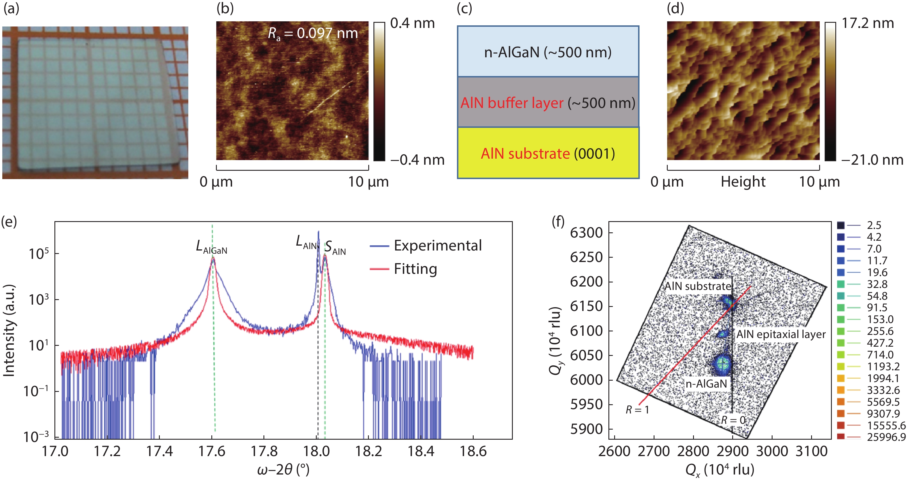
Table 1. FWHMs of (002) and (102) reflection peaks in the substrate and epitaxial layer.
| AlN substrate | AlN buffer layer | AlxGa1–xN epitaxial layer | |
| (002) | 65 arcsec | 93 arcsec | 202 arcsec |
| (102) | 36 arcsec | 29 arcsec | 496 arcsec |
 DownLoad: CSV
| [1] |
Hartmann C, Dittmar A, Wollweber J, et al. Bulk AlN growth by physical vapour transport. Semicond Sci Technol, 2014, 29, 084002 doi: 10.1088/0268-1242/29/8/084002
|
| [2] |
Filip O, Epelbaum B M, Bickermann M, et al. Effects of growth direction and polarity on bulk aluminum nitride crystal properties. J Cryst Growth, 2011, 318, 427 doi: 10.1016/j.jcrysgro.2010.10.198
|
| [3] |
Slack G A, McNelly T F. Growth of high purity AlN crystals. J Cryst Growth, 1976, 34, 263 doi: 10.1016/0022-0248(76)90139-1
|
| [4] |
Mokhov E, Izmaylova I, Kazarova O, et al. Specific features of sublimation growth of bulk AlN crystals on SiC wafers. Phys Status Solidi C, 2013, 10, 445 doi: 10.1002/pssc.201200638
|
| [5] |
Bickermann M, Filip O, Epelbaum B M, et al. Growth of AlN bulk crystals on SiC seeds: Chemical analysis and crystal properties. J Cryst Growth, 2012, 339, 13 doi: 10.1016/j.jcrysgro.2011.11.043
|
| [6] |
Nagai I, Kato T, Miura T, et al. AlN bulk single crystal growth on 6H-SiC substrates by sublimation method. J Cryst Growth, 2010, 312, 2699 doi: 10.1016/j.jcrysgro.2010.05.044
|
| [7] |
Hartmann C, Albrecht M, Wollweber J, et al. SiC seed polarity-dependent bulk AlN growth under the influence of residual oxygen. J Cryst Growth, 2012, 344, 19 doi: 10.1016/j.jcrysgro.2012.01.045
|
| [8] |
Chemekova T Y, Avdeev O V, Barash I S, et al. Sublimation growth of 2 inch diameter bulk AlN crystals. Phys Status Solidi C, 2008, 5, 1612 doi: 10.1002/pssc.200778534
|
| [9] |
Bickermann M, Epelbaum B M, Filip O, et al. Faceting in AlN bulk crystal growth and its impact on optical properties of the crystals. Phys Status Solidi C, 2012, 9, 449 doi: 10.1002/pssc.201100345
|
| [10] |
Sumathi R R, Barz R U, Straubinger T, et al. Structural and surface topography analysis of AlN single crystals grown on 6H-SiC substrates. J Cryst Growth, 2012, 360, 193 doi: 10.1016/j.jcrysgro.2011.11.054
|
| [11] |
Dalmau R, Craft H S, Britt J, et al. High quality AlN single crystal substrates for AlGaN-based devices. Mater Sci Forum, 2018, 924, 923 doi: 10.4028/www.scientific.net/MSF.924.923
|
| [12] |
Hartmann C, Matiwe L, Wollweber J, et al. Favourable growth conditions for the preparation of bulk AlN single crystals by PVT. CrystEngComm, 2020, 22, 1762 doi: 10.1039/C9CE01952A
|
| [13] |
Sumathi R R. Bulk AlN single crystal growth on foreign substrate and preparation of free-standing native seeds. CrystEngComm, 2013, 15, 2232 doi: 10.1039/C2CE26599K
|
| [14] |
Zhang L, Qi H T, Cheng H J, et al. Preparation and characterization of AlN seeds for homogeneous growth. J Semicond, 2019, 40, 102801 doi: 10.1088/40/10/102801
|
| [15] |
Bickermann M, Epelbaum B M, Filip O, et al. Deep-UV transparent bulk single-crystalline AlN substrates. Phys Status Solidi C, 2010, 7, 1743 doi: 10.1002/pssc.200983422
|
| [16] |
Bickermann M, Epelbaum B M, Filip O, et al. UV transparent single-crystalline bulk AlN substrates. Phys Status Solidi C, 2010, 7, 21 doi: 10.1002/pssc.200982601
|
| [17] |
Yang W X, Zhao Y K, Wu Y Y, et al. Deep-UV emission at 260 nm from MBE-grown AlGaN/AlN quantum-well structures. J Cryst Growth, 2019, 512, 213 doi: 10.1016/j.jcrysgro.2019.02.037
|
| [18] |
Bobea Graziano M, Bryan I, Bryan Z, et al. Structural characteristics of m-plane AlN substrates and homoepitaxial films. J Cryst Growth, 2019, 507, 389 doi: 10.1016/j.jcrysgro.2018.07.012
|
| [19] |
Zheng W, Zheng R S, Huang F, et al. Raman tensor of AlN bulk single crystal. Photon Res, 2015, 3, 38 doi: 10.1364/PRJ.3.000038
|
| [20] |
Lu P, Collazo R, Dalmau R F, et al. Seeded growth of AlN bulk crystals in m- and c-orientation. J Cryst Growth, 2009, 312, 58 doi: 10.1016/j.jcrysgro.2009.10.008
|
| [21] |
Jiang K, Sun X J, Ben J W, et al. Suppressing the compositional non-uniformity of AlGaN grown on a HVPE-AlN template with large macro-steps. CrystEngComm, 2019, 21, 4864 doi: 10.1039/C9CE00608G
|


Article views: 5279 Times PDF downloads: 176 Times Cited by: 0 Times
Received: 27 July 2020 Revised: 10 December 2020 Online: Accepted Manuscript: 15 March 2021Uncorrected proof: 16 March 2021Published: 01 May 2021
| Citation: |
Li Zhang, Haitao Qi, Hongjuan Cheng, Yuezeng Shi, Zhanpin Lai, Muchang Luo. Morphology and crystalline property of an AlN single crystal grown on AlN seed[J]. Journal of Semiconductors, 2021, 42(5): 052101. doi: 10.1088/1674-4926/42/5/052101
****
L Zhang, H T Qi, H J Cheng, Y Z Shi, Z P Lai, M C Luo, Morphology and crystalline property of an AlN single crystal grown on AlN seed[J]. J. Semicond., 2021, 42(5): 052101. doi: 10.1088/1674-4926/42/5/052101.

|
| [1] |
Hartmann C, Dittmar A, Wollweber J, et al. Bulk AlN growth by physical vapour transport. Semicond Sci Technol, 2014, 29, 084002 doi: 10.1088/0268-1242/29/8/084002
|
| [2] |
Filip O, Epelbaum B M, Bickermann M, et al. Effects of growth direction and polarity on bulk aluminum nitride crystal properties. J Cryst Growth, 2011, 318, 427 doi: 10.1016/j.jcrysgro.2010.10.198
|
| [3] |
Slack G A, McNelly T F. Growth of high purity AlN crystals. J Cryst Growth, 1976, 34, 263 doi: 10.1016/0022-0248(76)90139-1
|
| [4] |
Mokhov E, Izmaylova I, Kazarova O, et al. Specific features of sublimation growth of bulk AlN crystals on SiC wafers. Phys Status Solidi C, 2013, 10, 445 doi: 10.1002/pssc.201200638
|
| [5] |
Bickermann M, Filip O, Epelbaum B M, et al. Growth of AlN bulk crystals on SiC seeds: Chemical analysis and crystal properties. J Cryst Growth, 2012, 339, 13 doi: 10.1016/j.jcrysgro.2011.11.043
|
| [6] |
Nagai I, Kato T, Miura T, et al. AlN bulk single crystal growth on 6H-SiC substrates by sublimation method. J Cryst Growth, 2010, 312, 2699 doi: 10.1016/j.jcrysgro.2010.05.044
|
| [7] |
Hartmann C, Albrecht M, Wollweber J, et al. SiC seed polarity-dependent bulk AlN growth under the influence of residual oxygen. J Cryst Growth, 2012, 344, 19 doi: 10.1016/j.jcrysgro.2012.01.045
|
| [8] |
Chemekova T Y, Avdeev O V, Barash I S, et al. Sublimation growth of 2 inch diameter bulk AlN crystals. Phys Status Solidi C, 2008, 5, 1612 doi: 10.1002/pssc.200778534
|
| [9] |
Bickermann M, Epelbaum B M, Filip O, et al. Faceting in AlN bulk crystal growth and its impact on optical properties of the crystals. Phys Status Solidi C, 2012, 9, 449 doi: 10.1002/pssc.201100345
|
| [10] |
Sumathi R R, Barz R U, Straubinger T, et al. Structural and surface topography analysis of AlN single crystals grown on 6H-SiC substrates. J Cryst Growth, 2012, 360, 193 doi: 10.1016/j.jcrysgro.2011.11.054
|
| [11] |
Dalmau R, Craft H S, Britt J, et al. High quality AlN single crystal substrates for AlGaN-based devices. Mater Sci Forum, 2018, 924, 923 doi: 10.4028/www.scientific.net/MSF.924.923
|
| [12] |
Hartmann C, Matiwe L, Wollweber J, et al. Favourable growth conditions for the preparation of bulk AlN single crystals by PVT. CrystEngComm, 2020, 22, 1762 doi: 10.1039/C9CE01952A
|
| [13] |
Sumathi R R. Bulk AlN single crystal growth on foreign substrate and preparation of free-standing native seeds. CrystEngComm, 2013, 15, 2232 doi: 10.1039/C2CE26599K
|
| [14] |
Zhang L, Qi H T, Cheng H J, et al. Preparation and characterization of AlN seeds for homogeneous growth. J Semicond, 2019, 40, 102801 doi: 10.1088/40/10/102801
|
| [15] |
Bickermann M, Epelbaum B M, Filip O, et al. Deep-UV transparent bulk single-crystalline AlN substrates. Phys Status Solidi C, 2010, 7, 1743 doi: 10.1002/pssc.200983422
|
| [16] |
Bickermann M, Epelbaum B M, Filip O, et al. UV transparent single-crystalline bulk AlN substrates. Phys Status Solidi C, 2010, 7, 21 doi: 10.1002/pssc.200982601
|
| [17] |
Yang W X, Zhao Y K, Wu Y Y, et al. Deep-UV emission at 260 nm from MBE-grown AlGaN/AlN quantum-well structures. J Cryst Growth, 2019, 512, 213 doi: 10.1016/j.jcrysgro.2019.02.037
|
| [18] |
Bobea Graziano M, Bryan I, Bryan Z, et al. Structural characteristics of m-plane AlN substrates and homoepitaxial films. J Cryst Growth, 2019, 507, 389 doi: 10.1016/j.jcrysgro.2018.07.012
|
| [19] |
Zheng W, Zheng R S, Huang F, et al. Raman tensor of AlN bulk single crystal. Photon Res, 2015, 3, 38 doi: 10.1364/PRJ.3.000038
|
| [20] |
Lu P, Collazo R, Dalmau R F, et al. Seeded growth of AlN bulk crystals in m- and c-orientation. J Cryst Growth, 2009, 312, 58 doi: 10.1016/j.jcrysgro.2009.10.008
|
| [21] |
Jiang K, Sun X J, Ben J W, et al. Suppressing the compositional non-uniformity of AlGaN grown on a HVPE-AlN template with large macro-steps. CrystEngComm, 2019, 21, 4864 doi: 10.1039/C9CE00608G
|

 WeChat ID
Journal of Semiconductors © 2017 All Rights Reserved 京ICP备05085259号-2


