


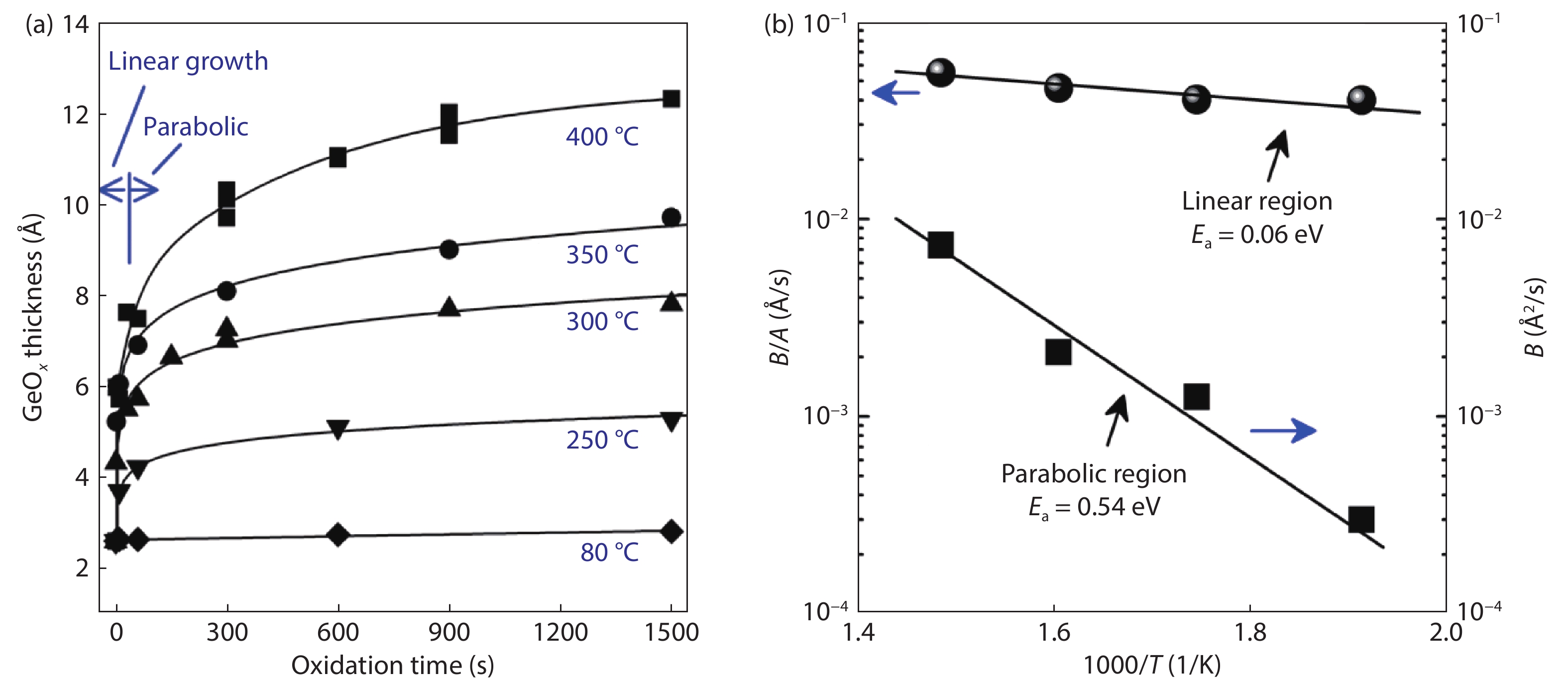
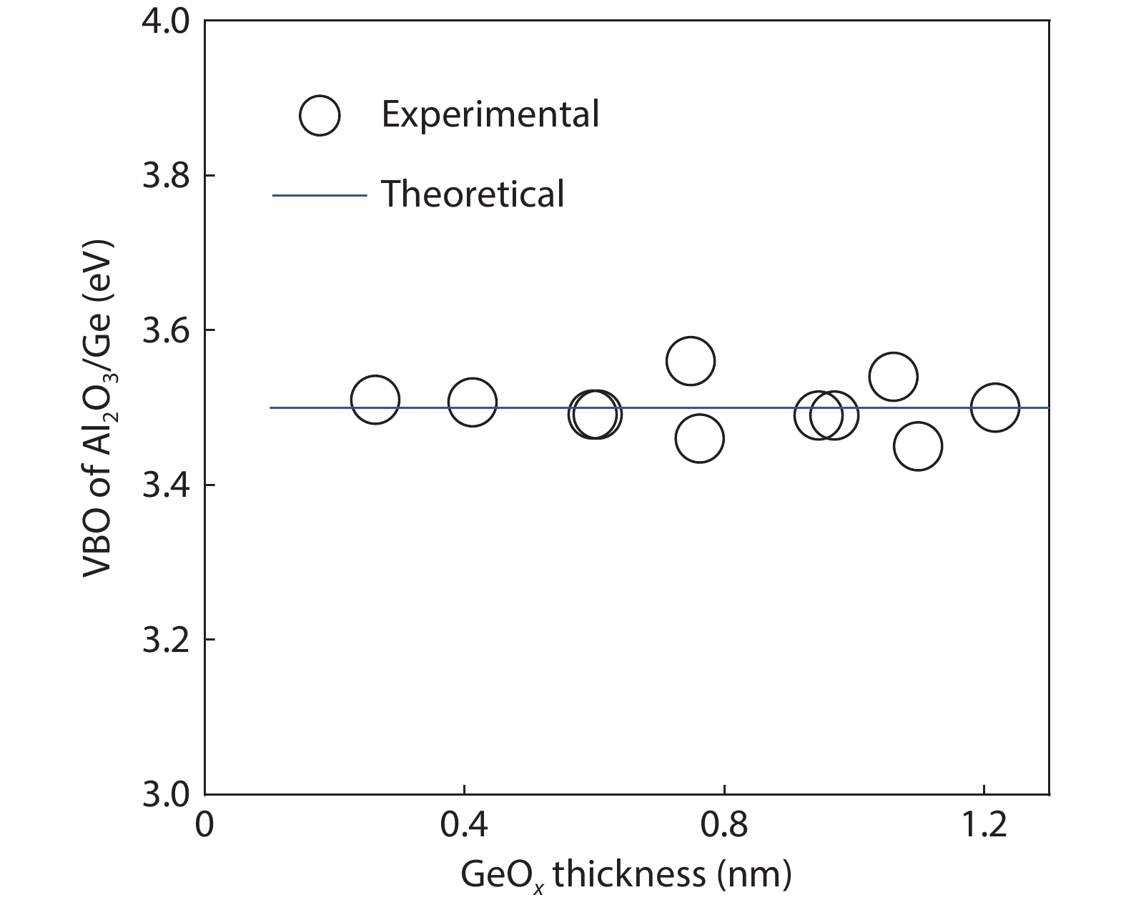
Fig. 1.
(a) GeOx thickness with oxidation time at temperature varying from 80 to 400 °C. (b) Arrhenius plots for linear and parabolic region. Ea is activation energy.
REVIEWS
Lixing Zhou1, Jinjuan Xiang2, , Xiaolei Wang2, and Wenwu Wang2
Corresponding author: Jinjuan Xiang, xiangjinjuan@ime.ac.cn; Xiaolei Wang, wangxiaolei@ime.ac.cn
Abstract:
Ge has been an alternative channel material for the performance enhancement of complementary metal–oxide–semiconductor (CMOS) technology applications because of its high carrier mobility and superior compatibility with Si CMOS technology. The gate structure plays a key role on the electrical property. In this paper, the property of Ge MOSFET with Al2O3/GeOx/Ge stack by ozone oxidation is reviewed. The GeOx passivation mechanism by ozone oxidation and band alignment of Al2O3/GeOx/Ge stack is described. In addition, the charge distribution in the gate stack and remote Coulomb scattering on carrier mobility is also presented. The surface passivation is mainly attributed to the high oxidation state of Ge. The energy band alignment is well explained by the gap state theory. The charge distribution is quantitatively characterized and it is found that the gate charges make a great degradation on carrier mobility. These investigations help to provide an impressive understanding and a possible instructive method to improve the performance of Ge devices.
Keywords: Ge MOSFET, ozone oxidation, gate charges, mobility
| [1] |
Kobayashi M, Thareja G, Ishibashi M, et al. Radical oxidation of germanium for interface gate dielectric GeO2 formation in metal-insulator-semiconductor gate stack. J Appl Phys, 2009, 106, 104117 doi: 10.1063/1.3259407
|
| [2] |
Takagi S, Zhang R, Suh J, et al. III–V/Ge channel MOS device technologies in nano CMOS era. Jpn J Appl Phys, 2015, 54, 06FA01 doi: 10.7567/JJAP.54.06FA01
|
| [3] |
Otani Y, Itayama Y, Tanaka T, et al. Fabrication of Ta2O5/GeNx gate insulator stack for Ge metal-insulator-semiconductor structures by electron-cyclotron-resonance plasma nitridation and sputtering deposition techniques. Appl Phys Lett, 2007, 90, 142114 doi: 10.1063/1.2720345
|
| [4] |
Maeda T, Nishizawa M, Morita Y, et al. Role of germanium nitride interfacial layers in HfO2/germanium nitride/germanium metal-insulator-semiconductor structures. Appl Phys Lett, 2007, 90, 072911 doi: 10.1063/1.2679941
|
| [5] |
Kim K H, Gordon R G, Ritenour A, et al. Atomic layer deposition of insulating nitride interfacial layers for germanium metal oxide semiconductor field effect transistors with high-κ oxide/tungsten nitride gate stacks. Appl Phys Lett, 2007, 90, 212104 doi: 10.1063/1.2741609
|
| [6] |
Hashemi P, Hoyt J L. High hole-mobility strained- Ge/Si0.6Ge0.4 P-MOSFETs with high-K/metal gate: Role of strained-Si cap thickness. IEEE Electron Device Lett, 2012, 33, 173 doi: 10.1109/LED.2011.2176913
|
| [7] |
Chen W B, Chin A. High performance of Ge nMOSFETs using SiO2 interfacial layer and TiLaO gate dielectric. IEEE Electron Device Lett, 2010, 31, 80 doi: 10.1109/LED.2009.2035719
|
| [8] |
Matsubara H, Sasada T, Takenaka M, et al. Evidence of low interface trap density in GeO2/Ge metal-oxide-semiconductor structures fabricated by thermal oxidation. Appl Phys Lett, 2008, 93, 032104 doi: 10.1063/1.2959731
|
| [9] |
Xie Q, Deduytsche D, Schaekers M, et al. Effective electrical passivation of Ge(100) for HfO2 gate dielectric layers using O2 plasma. Electrochem Solid-State Lett, 2011, 14, G20 doi: 10.1149/1.3551461
|
| [10] |
Kuzum D, Krishnamohan T, Pethe A J, et al. Ge-interface engineering with ozone oxidation for low interface-state density. IEEE Electron Device Lett, 2008, 29, 328 doi: 10.1109/LED.2008.918272
|
| [11] |
Fukuda Y, Ueno T, Hirono S, et al. Electrical characterization of germanium oxide/germanium interface prepared by electron-cyclotron-resonance plasma irradiation. Jpn J Appl Phys, 2005, 44, 6981 doi: 10.1143/JJAP.44.6981
|
| [12] |
Fukuda Y, Yazaki Y, Otani Y, et al. Low-temperature formation of high-quality GeO2 interlayer for high-k gate dielectrics/Ge by electron-cyclotron-resonance plasma techniques. IEEE Trans Electron Devices, 2010, 57, 282 doi: 10.1109/TED.2009.2035030
|
| [13] |
Lee C H, Nishimura T, Nagashio K, et al. High-electron-mobility Ge/GeO2 n-MOSFETs with two-step oxidation. IEEE Trans Electron Devices, 2011, 58, 1295 doi: 10.1109/TED.2011.2111373
|
| [14] |
Zhang R, Iwasaki T, Taoka N, et al. High-mobility Ge pMOSFET with 1-nm EOT Al2O3/GeOx/Ge gate stack fabricated by plasma post oxidation. IEEE Trans Electron Devices, 2012, 59, 335 doi: 10.1109/TED.2011.2176495
|
| [15] |
Zhang R, Huang P C, Lin J C, et al. High-mobility Ge p- and n-MOSFETs with 0.7-nm EOT using HfO2/Al2O3/GeOx/Ge gate stacks fabricated by plasma postoxidation. IEEE Trans Electron Devices, 2013, 60, 927 doi: 10.1109/TED.2013.2238942
|
| [16] |
Zhang R, Lin J C, Yu X, et al. Examination of physical origins limiting effective mobility of Ge MOSFETs and the improvement by atomic deuterium annealing. IEEE Symposium on VLSI Technology, 2013, 26
|
| [17] |
Lee C H, Lu C, Nishimura T, et al. Thermally robust CMOS-aware Ge MOSFETs with high mobility at high-carrier densities on a single orientation Ge substrate. 2014 Symposium on VLSI Technology (VLSI-Technology), 2014, 1 doi: 10.1109/VLSIT.2014.6894394
|
| [18] |
Lee C H, Nishimura T, Lu C, et al. Dramatic effects of hydrogen-induced out-diffusion of oxygen from Ge surface on junction leak. IEEE International Electron Devices Meeting, 2014, 32.5.1 doi: 10.1109/IEDM.2014.7047156
|
| [19] |
Wang X L, Xiang J J, Wang S K, et al. Remote interfacial dipole scattering and electron mobility degradation in Ge field-effect transistors with GeOx/Al2O3 gate dielectrics. J Phys D, 2016, 49, 255104 doi: 10.1088/0022-3727/49/25/255104
|
| [20] |
Zhou L X, Wang X L, Ma X L, et al. Hole mobility degradation by remote Coulomb scattering and charge distribution in Al2O3/GeOx gate stacks in bulk Ge pMOSFET with GeOx grown by ozone oxidation. J Phys D, 2017, 50, 245102 doi: 10.1088/1361-6463/aa6f96
|
| [21] |
Zhang R, Lin J C, Yu X, et al. Impact of plasma postoxidation temperature on the electrical properties of Al2O3/GeOx/Ge pMOSFETs and nMOSFETs. IEEE Trans Electron Devices, 2014, 61, 416 doi: 10.1109/TED.2013.2295822
|
| [22] |
Esseni D, Abramo A. Modeling of electron mobility degradation by remote Coulomb scattering in ultrathin oxide MOSFETs. IEEE Trans Electron Devices, 2003, 50, 1665 doi: 10.1109/TED.2003.814973
|
| [23] |
Saito S I, Torii K, Shimamoto Y, et al. Remote-charge-scattering limited mobility in field-effect transistors with SiO2 and Al2O3/SiO2 gate stacks. J Appl Phys, 2005, 98, 113706 doi: 10.1063/1.2135878
|
| [24] |
Casterman D, de Souza M M. Evaluation of the Coulomb-limited mobility in high-κ dielectric metal oxide semiconductor field effect transistors. J Appl Phys, 2010, 107, 063706 doi: 10.1063/1.3319558
|
| [25] |
Kaushik V S, O'Sullivan B J, Pourtois G, et al. Estimation of fixed charge densities in hafnium-silicate gate dielectrics. IEEE Trans Electron Devices, 2006, 53, 2627 doi: 10.1109/TED.2006.882412
|
| [26] |
Ota H, Hirano A, Watanabe Y, et al. Intrinsic origin of electron mobility reduction in high-k MOSFETs - from remote phonon to bottom interface dipole scattering. 2007 IEEE International Electron Devices Meeting, 2007, 65 doi: 10.1109/IEDM.2007.4418864
|
| [27] |
Jha R, Gurganos J, Kim Y H, et al. A capacitance-based methodology for work function extraction of metals on high-k. IEEE Electron Device Lett, 2004, 25, 420 doi: 10.1109/LED.2004.829032
|
| [28] |
Wang X L, Han K, Wang W W, et al. Physical origin of dipole formation at high-k/SiO2 interface in metal-oxide-semiconductor device with high-k/metal gate structure. Appl Phys Lett, 2010, 96, 152907 doi: 10.1063/1.3399359
|
| [29] |
Wang X L, Han K, Wang W W, et al. Comprehensive understanding of the effect of electric dipole at high-k/SiO2 interface on the flatband voltage shift in metal-oxide-semiconductor device. Appl Phys Lett, 2010, 97, 062901 doi: 10.1063/1.3475774
|
| [30] |
Barraud S, Bonno O, Cassé M. The influence of Coulomb centers located in HfO2/SiO2 gate stacks on the effective electron mobility. J Appl Phys, 2008, 104, 073725 doi: 10.1063/1.2968217
|
| [31] |
Toniutti P, Palestri P, Esseni D, et al. On the origin of the mobility reduction in n- and p-metal-oxide-semiconductor field effect transistors with hafnium-based/metal gate stacks. J Appl Phys, 2012, 112, 034502 doi: 10.1063/1.4737781
|
| [32] |
Bellenger F, Houssa M, Delabie A, et al. Passivation of Ge(100)/GeO2/high-κ gate stacks using thermal oxide treatments. J Electrochem Soc, 2008, 155, G33 doi: 10.1149/1.2819626
|
| [33] |
Deng S R, Xie Q, Deduytsche D, et al. Effective reduction of fixed charge densities in germanium based metal-oxide-semiconductor devices. Appl Phys Lett, 2011, 99, 052906 doi: 10.1063/1.3622649
|
| [34] |
Prabhakaran K, Maeda F, Watanabe Y, et al. Distinctly different thermal decomposition pathways of ultrathin oxide layer on Ge and Si surfaces. Appl Phys Lett, 2000, 76, 2244 doi: 10.1063/1.126309
|
| [35] |
Wang S, Kita K, Lee C H, et al. Desorption kinetics of GeO from GeO2/Ge structure. J Appl Phys, 2010, 108, 054104 doi: 10.1063/1.3475990
|
| [36] |
Plummer J D, Deal M D, Griffin P B. Silicon VLSI technology: Fundamentals, practice, and modeling. Prentice Hal, 2001
|
| [37] |
Cui Z J, Takoudis C G. Initial oxidation of H-terminated Si(100) in O3 (950 ppm)/O2 and pure O2. J Electrochem Soc, 2003, 150, G694 doi: 10.1149/1.1613295
|
| [38] |
Fink C K, Jenkins S J. Radical-mediated adsorption: Ozone oxidation of passivated silicon. Surf Sci, 2008, 602, L100 doi: 10.1016/j.susc.2008.05.028
|
| [39] |
Bulanin K M, Alexeev A V, Bystrov D S, et al. IR study of ozone adsorption on SiO2. J Phys Chem, 1994, 98, 5100 doi: 10.1021/j100070a026
|
| [40] |
Sun S Y, Sun Y, Liu Z, et al. Roles of oxygen and water vapor in the oxidation of halogen terminated Ge(111) surfaces. Appl Phys Lett, 2006, 89, 231925 doi: 10.1063/1.2403908
|
| [41] |
Renault O, Fourdrinier L, Martinez E, et al. High-resolution photoelectron spectroscopy of Ge-based HfO2 gate stacks. Appl Phys Lett, 2007, 90, 052112 doi: 10.1063/1.2435512
|
| [42] |
Kato K, Kyogoku S, Sakashita M, et al. Control of interfacial properties of Al2O3/Ge gate stack structure using radical nitridation technique. Jpn J Appl Phys, 2011, 50, 10PE02 doi: 10.7567/JJAP.50.10PE02
|
| [43] |
Sahari S K, Murakami H, Fujioka T, et al. Native oxidation growth on Ge(111) and (100) surfaces. Jpn J Appl Phys, 2011, 50, 04DA12 doi: 10.7567/JJAP.50.04DA12
|
| [44] |
He G, Zhu L Q, Sun Z Q, et al. Integrations and challenges of novel high-k gate stacks in advanced CMOS technology. Prog Mater Sci, 2011, 56, 475 doi: 10.1016/j.pmatsci.2011.01.012
|
| [45] |
He G, Chen X S, Sun Z Q. Interface engineering and chemistry of Hf-based high-k dielectrics on III–V substrates. Surf Sci Rep, 2013, 68, 68 doi: 10.1016/j.surfrep.2013.01.002
|
| [46] |
Zhang J W, He G, Liu M, et al. Composition dependent interfacial thermal stability, band alignment and electrical properties of Hf1−xTixO2/Si gate stacks. Appl Surf Sci, 2015, 346, 489 doi: 10.1016/j.apsusc.2015.03.171
|
| [47] |
Hudait M K, Zhu Y, Maurya D, et al. Structural and band alignment properties of Al2O3 on epitaxial Ge grown on (100), (110), and (111)A GaAs substrates by molecular beam epitaxy. J Appl Phys, 2013, 113, 134311 doi: 10.1063/1.4799367
|
| [48] |
Swaminathan S, Sun Y, Pianetta P, et al. Ultrathin ALD-Al2O3 layers for Ge(001) gate stacks: Local composition evolution and dielectric properties. J Appl Phys, 2011, 110, 094105 doi: 10.1063/1.3647761
|
| [49] |
Chellappan R K, Rao Gajula D, McNeill D, et al. Soft X-ray photoemission study of the thermal stability of the Al2O3/Ge (100) interface as a function of surface preparation. J Appl Phys, 2013, 114, 084312 doi: 10.1063/1.4819214
|
| [50] |
Fulton C C, Lucovsky G, Nemanich R J. Electronic properties of the Zr-ZrO2-SiO2-Si(100) gate stack structure. J Appl Phys, 2006, 99, 063708 doi: 10.1063/1.2181282
|
| [51] |
Afanas'ev V V, Stesmans A, Chen F, et al. Internal photoemission of electrons and holes from (100)Si into HfO2. Appl Phys Lett, 2002, 81, 1053 doi: 10.1063/1.1495088
|
| [52] |
Afanas'ev V V, Stesmans A. Energy band alignment at the (100)Ge/HfO2 interface. Appl Phys Lett, 2004, 84, 2319 doi: 10.1063/1.1688453
|
| [53] |
Yang J L, Eller B S, Zhu C Y, et al. Comparative band alignment of plasma-enhanced atomic layer deposited high-k dielectrics on gallium nitride. J Appl Phys, 2012, 112, 053710 doi: 10.1063/1.4749268
|
| [54] |
Perego M, Seguini G, Scarel G, et al. Energy band alignment at TiO2/Si interface with various interlayers. J Appl Phys, 2008, 103, 043509 doi: 10.1063/1.2885109
|
| [55] |
Kraut E A, Grant R W, Waldrop J R, et al. Precise determination of the valence-band edge in X-ray photoemission spectra: Application to measurement of semiconductor interface potentials. Phys Rev Lett, 1980, 44, 1620 doi: 10.1103/PhysRevLett.44.1620
|
| [56] |
Tersoff J. Theory of semiconductor heterojunctions: The role of quantum dipoles. Phys Rev B, 1984, 30, 4874 doi: 10.1103/PhysRevB.30.4874
|
| [57] |
Mönch W. Branch-point energies and the band-structure lineup at Schottky contacts and heterostrucures. J Appl Phys, 2011, 109, 113724 doi: 10.1063/1.3592978
|
| [58] |
Robertson J, Falabretti B. Band offsets of high K gate oxides on III-V semiconductors. J Appl Phys, 2006, 100, 014111 doi: 10.1063/1.2213170
|
| [59] |
Mönch W. On the electric-dipole contribution to the valence-band offsets in semiconductor-oxide heterostructures. Appl Phys Lett, 2007, 91, 042117 doi: 10.1063/1.2760176
|
| [60] |
Robertson J, Falabretti B. Band offsets of high K gate oxides on high mobility semiconductors. Mater Sci Eng B, 2006, 135, 267 doi: 10.1016/j.mseb.2006.08.017
|
| [61] |
Robertson J. Band offsets of high dielectric constant gate oxides on silicon. J Non Cryst Solids, 2002, 303, 94 doi: 10.1016/S0022-3093(02)00972-9
|
| [62] |
Pourtois G, Houssa M, De Jaeger B, et al. Threshold voltage shifts in Si passivated (100)Ge p-channel field effect transistors: Insights from first-principles modeling. Appl Phys Lett, 2007, 91, 023506 doi: 10.1063/1.2756367
|
| [63] |
Kaczer B, Franco J, Mitard J, et al. Improvement in NBTI reliability of Si-passivated Ge/high-k/metal-gate pFETs. Microelectron Eng, 2009, 86, 1582 doi: 10.1016/j.mee.2009.03.061
|
| [64] |
Choi M, Janotti A, van de Walle C G. Native point defects and dangling bonds in α-Al2O3. J Appl Phys, 2013, 113, 044501 doi: 10.1063/1.4784114
|
| [65] |
Wang X L, Xiang J J, Wang W W, et al. Dependence of electrostatic potential distribution of Al2O3/Ge structure on Al2O3 thickness. Surf Sci, 2016, 651, 94 doi: 10.1016/j.susc.2016.04.001
|
| [66] |
Zhou L X, Wang X L, Han K, et al. Experimental investigation of remote coulomb scattering on mobility degradation of Ge pMOSFET by various PDA ambiences. IEEE Trans Electron Devices, 2019, 66, 1669 doi: 10.1109/TED.2019.2900801
|


Article views: 5657 Times PDF downloads: 282 Times Cited by: 0 Times
Received: 18 May 2021 Revised: 21 June 2021 Online: Uncorrected proof: 03 September 2021Accepted Manuscript: 03 September 2021Published: 04 January 2022
| Citation: |
Lixing Zhou, Jinjuan Xiang, Xiaolei Wang, Wenwu Wang. Investigation on the passivation, band alignment, gate charge, and mobility degradation of the Ge MOSFET with a GeOx/Al2O3 gate stack by ozone oxidation[J]. Journal of Semiconductors, 2022, 43(1): 013101. doi: 10.1088/1674-4926/43/1/013101
****
L X Zhou, J J Xiang, X L Wang, W W Wang, Investigation on the passivation, band alignment, gate charge, and mobility degradation of the Ge MOSFET with a GeOx/Al2O3 gate stack by ozone oxidation[J]. J. Semicond., 2022, 43(1): 013101. doi: 10.1088/1674-4926/43/1/013101.

|
Ge has been an alternative channel material for the performance enhancement of complementary metal–oxide–semiconductor (CMOS) technology applications because of its high carrier mobility and superior compatibility with Si CMOS technology. The gate structure plays a key role on the electrical property. In this paper, the property of Ge MOSFET with Al2O3/GeOx/Ge stack by ozone oxidation is reviewed. The GeOx passivation mechanism by ozone oxidation and band alignment of Al2O3/GeOx/Ge stack is described. In addition, the charge distribution in the gate stack and remote Coulomb scattering on carrier mobility is also presented. The surface passivation is mainly attributed to the high oxidation state of Ge. The energy band alignment is well explained by the gap state theory. The charge distribution is quantitatively characterized and it is found that the gate charges make a great degradation on carrier mobility. These investigations help to provide an impressive understanding and a possible instructive method to improve the performance of Ge devices.
| [1] |
Kobayashi M, Thareja G, Ishibashi M, et al. Radical oxidation of germanium for interface gate dielectric GeO2 formation in metal-insulator-semiconductor gate stack. J Appl Phys, 2009, 106, 104117 doi: 10.1063/1.3259407
|
| [2] |
Takagi S, Zhang R, Suh J, et al. III–V/Ge channel MOS device technologies in nano CMOS era. Jpn J Appl Phys, 2015, 54, 06FA01 doi: 10.7567/JJAP.54.06FA01
|
| [3] |
Otani Y, Itayama Y, Tanaka T, et al. Fabrication of Ta2O5/GeNx gate insulator stack for Ge metal-insulator-semiconductor structures by electron-cyclotron-resonance plasma nitridation and sputtering deposition techniques. Appl Phys Lett, 2007, 90, 142114 doi: 10.1063/1.2720345
|
| [4] |
Maeda T, Nishizawa M, Morita Y, et al. Role of germanium nitride interfacial layers in HfO2/germanium nitride/germanium metal-insulator-semiconductor structures. Appl Phys Lett, 2007, 90, 072911 doi: 10.1063/1.2679941
|
| [5] |
Kim K H, Gordon R G, Ritenour A, et al. Atomic layer deposition of insulating nitride interfacial layers for germanium metal oxide semiconductor field effect transistors with high-κ oxide/tungsten nitride gate stacks. Appl Phys Lett, 2007, 90, 212104 doi: 10.1063/1.2741609
|
| [6] |
Hashemi P, Hoyt J L. High hole-mobility strained- Ge/Si0.6Ge0.4 P-MOSFETs with high-K/metal gate: Role of strained-Si cap thickness. IEEE Electron Device Lett, 2012, 33, 173 doi: 10.1109/LED.2011.2176913
|
| [7] |
Chen W B, Chin A. High performance of Ge nMOSFETs using SiO2 interfacial layer and TiLaO gate dielectric. IEEE Electron Device Lett, 2010, 31, 80 doi: 10.1109/LED.2009.2035719
|
| [8] |
Matsubara H, Sasada T, Takenaka M, et al. Evidence of low interface trap density in GeO2/Ge metal-oxide-semiconductor structures fabricated by thermal oxidation. Appl Phys Lett, 2008, 93, 032104 doi: 10.1063/1.2959731
|
| [9] |
Xie Q, Deduytsche D, Schaekers M, et al. Effective electrical passivation of Ge(100) for HfO2 gate dielectric layers using O2 plasma. Electrochem Solid-State Lett, 2011, 14, G20 doi: 10.1149/1.3551461
|
| [10] |
Kuzum D, Krishnamohan T, Pethe A J, et al. Ge-interface engineering with ozone oxidation for low interface-state density. IEEE Electron Device Lett, 2008, 29, 328 doi: 10.1109/LED.2008.918272
|
| [11] |
Fukuda Y, Ueno T, Hirono S, et al. Electrical characterization of germanium oxide/germanium interface prepared by electron-cyclotron-resonance plasma irradiation. Jpn J Appl Phys, 2005, 44, 6981 doi: 10.1143/JJAP.44.6981
|
| [12] |
Fukuda Y, Yazaki Y, Otani Y, et al. Low-temperature formation of high-quality GeO2 interlayer for high-k gate dielectrics/Ge by electron-cyclotron-resonance plasma techniques. IEEE Trans Electron Devices, 2010, 57, 282 doi: 10.1109/TED.2009.2035030
|
| [13] |
Lee C H, Nishimura T, Nagashio K, et al. High-electron-mobility Ge/GeO2 n-MOSFETs with two-step oxidation. IEEE Trans Electron Devices, 2011, 58, 1295 doi: 10.1109/TED.2011.2111373
|
| [14] |
Zhang R, Iwasaki T, Taoka N, et al. High-mobility Ge pMOSFET with 1-nm EOT Al2O3/GeOx/Ge gate stack fabricated by plasma post oxidation. IEEE Trans Electron Devices, 2012, 59, 335 doi: 10.1109/TED.2011.2176495
|
| [15] |
Zhang R, Huang P C, Lin J C, et al. High-mobility Ge p- and n-MOSFETs with 0.7-nm EOT using HfO2/Al2O3/GeOx/Ge gate stacks fabricated by plasma postoxidation. IEEE Trans Electron Devices, 2013, 60, 927 doi: 10.1109/TED.2013.2238942
|
| [16] |
Zhang R, Lin J C, Yu X, et al. Examination of physical origins limiting effective mobility of Ge MOSFETs and the improvement by atomic deuterium annealing. IEEE Symposium on VLSI Technology, 2013, 26
|
| [17] |
Lee C H, Lu C, Nishimura T, et al. Thermally robust CMOS-aware Ge MOSFETs with high mobility at high-carrier densities on a single orientation Ge substrate. 2014 Symposium on VLSI Technology (VLSI-Technology), 2014, 1 doi: 10.1109/VLSIT.2014.6894394
|
| [18] |
Lee C H, Nishimura T, Lu C, et al. Dramatic effects of hydrogen-induced out-diffusion of oxygen from Ge surface on junction leak. IEEE International Electron Devices Meeting, 2014, 32.5.1 doi: 10.1109/IEDM.2014.7047156
|
| [19] |
Wang X L, Xiang J J, Wang S K, et al. Remote interfacial dipole scattering and electron mobility degradation in Ge field-effect transistors with GeOx/Al2O3 gate dielectrics. J Phys D, 2016, 49, 255104 doi: 10.1088/0022-3727/49/25/255104
|
| [20] |
Zhou L X, Wang X L, Ma X L, et al. Hole mobility degradation by remote Coulomb scattering and charge distribution in Al2O3/GeOx gate stacks in bulk Ge pMOSFET with GeOx grown by ozone oxidation. J Phys D, 2017, 50, 245102 doi: 10.1088/1361-6463/aa6f96
|
| [21] |
Zhang R, Lin J C, Yu X, et al. Impact of plasma postoxidation temperature on the electrical properties of Al2O3/GeOx/Ge pMOSFETs and nMOSFETs. IEEE Trans Electron Devices, 2014, 61, 416 doi: 10.1109/TED.2013.2295822
|
| [22] |
Esseni D, Abramo A. Modeling of electron mobility degradation by remote Coulomb scattering in ultrathin oxide MOSFETs. IEEE Trans Electron Devices, 2003, 50, 1665 doi: 10.1109/TED.2003.814973
|
| [23] |
Saito S I, Torii K, Shimamoto Y, et al. Remote-charge-scattering limited mobility in field-effect transistors with SiO2 and Al2O3/SiO2 gate stacks. J Appl Phys, 2005, 98, 113706 doi: 10.1063/1.2135878
|
| [24] |
Casterman D, de Souza M M. Evaluation of the Coulomb-limited mobility in high-κ dielectric metal oxide semiconductor field effect transistors. J Appl Phys, 2010, 107, 063706 doi: 10.1063/1.3319558
|
| [25] |
Kaushik V S, O'Sullivan B J, Pourtois G, et al. Estimation of fixed charge densities in hafnium-silicate gate dielectrics. IEEE Trans Electron Devices, 2006, 53, 2627 doi: 10.1109/TED.2006.882412
|
| [26] |
Ota H, Hirano A, Watanabe Y, et al. Intrinsic origin of electron mobility reduction in high-k MOSFETs - from remote phonon to bottom interface dipole scattering. 2007 IEEE International Electron Devices Meeting, 2007, 65 doi: 10.1109/IEDM.2007.4418864
|
| [27] |
Jha R, Gurganos J, Kim Y H, et al. A capacitance-based methodology for work function extraction of metals on high-k. IEEE Electron Device Lett, 2004, 25, 420 doi: 10.1109/LED.2004.829032
|
| [28] |
Wang X L, Han K, Wang W W, et al. Physical origin of dipole formation at high-k/SiO2 interface in metal-oxide-semiconductor device with high-k/metal gate structure. Appl Phys Lett, 2010, 96, 152907 doi: 10.1063/1.3399359
|
| [29] |
Wang X L, Han K, Wang W W, et al. Comprehensive understanding of the effect of electric dipole at high-k/SiO2 interface on the flatband voltage shift in metal-oxide-semiconductor device. Appl Phys Lett, 2010, 97, 062901 doi: 10.1063/1.3475774
|
| [30] |
Barraud S, Bonno O, Cassé M. The influence of Coulomb centers located in HfO2/SiO2 gate stacks on the effective electron mobility. J Appl Phys, 2008, 104, 073725 doi: 10.1063/1.2968217
|
| [31] |
Toniutti P, Palestri P, Esseni D, et al. On the origin of the mobility reduction in n- and p-metal-oxide-semiconductor field effect transistors with hafnium-based/metal gate stacks. J Appl Phys, 2012, 112, 034502 doi: 10.1063/1.4737781
|
| [32] |
Bellenger F, Houssa M, Delabie A, et al. Passivation of Ge(100)/GeO2/high-κ gate stacks using thermal oxide treatments. J Electrochem Soc, 2008, 155, G33 doi: 10.1149/1.2819626
|
| [33] |
Deng S R, Xie Q, Deduytsche D, et al. Effective reduction of fixed charge densities in germanium based metal-oxide-semiconductor devices. Appl Phys Lett, 2011, 99, 052906 doi: 10.1063/1.3622649
|
| [34] |
Prabhakaran K, Maeda F, Watanabe Y, et al. Distinctly different thermal decomposition pathways of ultrathin oxide layer on Ge and Si surfaces. Appl Phys Lett, 2000, 76, 2244 doi: 10.1063/1.126309
|
| [35] |
Wang S, Kita K, Lee C H, et al. Desorption kinetics of GeO from GeO2/Ge structure. J Appl Phys, 2010, 108, 054104 doi: 10.1063/1.3475990
|
| [36] |
Plummer J D, Deal M D, Griffin P B. Silicon VLSI technology: Fundamentals, practice, and modeling. Prentice Hal, 2001
|
| [37] |
Cui Z J, Takoudis C G. Initial oxidation of H-terminated Si(100) in O3 (950 ppm)/O2 and pure O2. J Electrochem Soc, 2003, 150, G694 doi: 10.1149/1.1613295
|
| [38] |
Fink C K, Jenkins S J. Radical-mediated adsorption: Ozone oxidation of passivated silicon. Surf Sci, 2008, 602, L100 doi: 10.1016/j.susc.2008.05.028
|
| [39] |
Bulanin K M, Alexeev A V, Bystrov D S, et al. IR study of ozone adsorption on SiO2. J Phys Chem, 1994, 98, 5100 doi: 10.1021/j100070a026
|
| [40] |
Sun S Y, Sun Y, Liu Z, et al. Roles of oxygen and water vapor in the oxidation of halogen terminated Ge(111) surfaces. Appl Phys Lett, 2006, 89, 231925 doi: 10.1063/1.2403908
|
| [41] |
Renault O, Fourdrinier L, Martinez E, et al. High-resolution photoelectron spectroscopy of Ge-based HfO2 gate stacks. Appl Phys Lett, 2007, 90, 052112 doi: 10.1063/1.2435512
|
| [42] |
Kato K, Kyogoku S, Sakashita M, et al. Control of interfacial properties of Al2O3/Ge gate stack structure using radical nitridation technique. Jpn J Appl Phys, 2011, 50, 10PE02 doi: 10.7567/JJAP.50.10PE02
|
| [43] |
Sahari S K, Murakami H, Fujioka T, et al. Native oxidation growth on Ge(111) and (100) surfaces. Jpn J Appl Phys, 2011, 50, 04DA12 doi: 10.7567/JJAP.50.04DA12
|
| [44] |
He G, Zhu L Q, Sun Z Q, et al. Integrations and challenges of novel high-k gate stacks in advanced CMOS technology. Prog Mater Sci, 2011, 56, 475 doi: 10.1016/j.pmatsci.2011.01.012
|
| [45] |
He G, Chen X S, Sun Z Q. Interface engineering and chemistry of Hf-based high-k dielectrics on III–V substrates. Surf Sci Rep, 2013, 68, 68 doi: 10.1016/j.surfrep.2013.01.002
|
| [46] |
Zhang J W, He G, Liu M, et al. Composition dependent interfacial thermal stability, band alignment and electrical properties of Hf1−xTixO2/Si gate stacks. Appl Surf Sci, 2015, 346, 489 doi: 10.1016/j.apsusc.2015.03.171
|
| [47] |
Hudait M K, Zhu Y, Maurya D, et al. Structural and band alignment properties of Al2O3 on epitaxial Ge grown on (100), (110), and (111)A GaAs substrates by molecular beam epitaxy. J Appl Phys, 2013, 113, 134311 doi: 10.1063/1.4799367
|
| [48] |
Swaminathan S, Sun Y, Pianetta P, et al. Ultrathin ALD-Al2O3 layers for Ge(001) gate stacks: Local composition evolution and dielectric properties. J Appl Phys, 2011, 110, 094105 doi: 10.1063/1.3647761
|
| [49] |
Chellappan R K, Rao Gajula D, McNeill D, et al. Soft X-ray photoemission study of the thermal stability of the Al2O3/Ge (100) interface as a function of surface preparation. J Appl Phys, 2013, 114, 084312 doi: 10.1063/1.4819214
|
| [50] |
Fulton C C, Lucovsky G, Nemanich R J. Electronic properties of the Zr-ZrO2-SiO2-Si(100) gate stack structure. J Appl Phys, 2006, 99, 063708 doi: 10.1063/1.2181282
|
| [51] |
Afanas'ev V V, Stesmans A, Chen F, et al. Internal photoemission of electrons and holes from (100)Si into HfO2. Appl Phys Lett, 2002, 81, 1053 doi: 10.1063/1.1495088
|
| [52] |
Afanas'ev V V, Stesmans A. Energy band alignment at the (100)Ge/HfO2 interface. Appl Phys Lett, 2004, 84, 2319 doi: 10.1063/1.1688453
|
| [53] |
Yang J L, Eller B S, Zhu C Y, et al. Comparative band alignment of plasma-enhanced atomic layer deposited high-k dielectrics on gallium nitride. J Appl Phys, 2012, 112, 053710 doi: 10.1063/1.4749268
|
| [54] |
Perego M, Seguini G, Scarel G, et al. Energy band alignment at TiO2/Si interface with various interlayers. J Appl Phys, 2008, 103, 043509 doi: 10.1063/1.2885109
|
| [55] |
Kraut E A, Grant R W, Waldrop J R, et al. Precise determination of the valence-band edge in X-ray photoemission spectra: Application to measurement of semiconductor interface potentials. Phys Rev Lett, 1980, 44, 1620 doi: 10.1103/PhysRevLett.44.1620
|
| [56] |
Tersoff J. Theory of semiconductor heterojunctions: The role of quantum dipoles. Phys Rev B, 1984, 30, 4874 doi: 10.1103/PhysRevB.30.4874
|
| [57] |
Mönch W. Branch-point energies and the band-structure lineup at Schottky contacts and heterostrucures. J Appl Phys, 2011, 109, 113724 doi: 10.1063/1.3592978
|
| [58] |
Robertson J, Falabretti B. Band offsets of high K gate oxides on III-V semiconductors. J Appl Phys, 2006, 100, 014111 doi: 10.1063/1.2213170
|
| [59] |
Mönch W. On the electric-dipole contribution to the valence-band offsets in semiconductor-oxide heterostructures. Appl Phys Lett, 2007, 91, 042117 doi: 10.1063/1.2760176
|
| [60] |
Robertson J, Falabretti B. Band offsets of high K gate oxides on high mobility semiconductors. Mater Sci Eng B, 2006, 135, 267 doi: 10.1016/j.mseb.2006.08.017
|
| [61] |
Robertson J. Band offsets of high dielectric constant gate oxides on silicon. J Non Cryst Solids, 2002, 303, 94 doi: 10.1016/S0022-3093(02)00972-9
|
| [62] |
Pourtois G, Houssa M, De Jaeger B, et al. Threshold voltage shifts in Si passivated (100)Ge p-channel field effect transistors: Insights from first-principles modeling. Appl Phys Lett, 2007, 91, 023506 doi: 10.1063/1.2756367
|
| [63] |
Kaczer B, Franco J, Mitard J, et al. Improvement in NBTI reliability of Si-passivated Ge/high-k/metal-gate pFETs. Microelectron Eng, 2009, 86, 1582 doi: 10.1016/j.mee.2009.03.061
|
| [64] |
Choi M, Janotti A, van de Walle C G. Native point defects and dangling bonds in α-Al2O3. J Appl Phys, 2013, 113, 044501 doi: 10.1063/1.4784114
|
| [65] |
Wang X L, Xiang J J, Wang W W, et al. Dependence of electrostatic potential distribution of Al2O3/Ge structure on Al2O3 thickness. Surf Sci, 2016, 651, 94 doi: 10.1016/j.susc.2016.04.001
|
| [66] |
Zhou L X, Wang X L, Han K, et al. Experimental investigation of remote coulomb scattering on mobility degradation of Ge pMOSFET by various PDA ambiences. IEEE Trans Electron Devices, 2019, 66, 1669 doi: 10.1109/TED.2019.2900801
|

 WeChat ID
Journal of Semiconductors © 2017 All Rights Reserved 京ICP备05085259号-2

 DownLoad:

