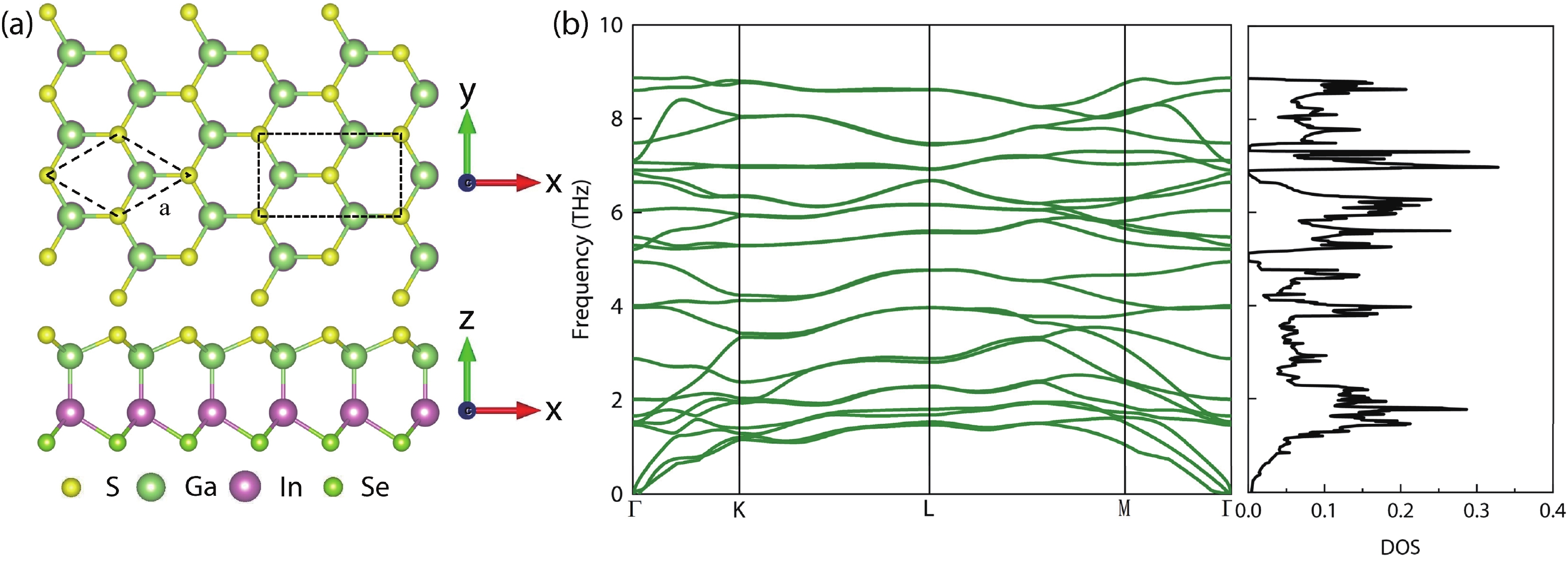
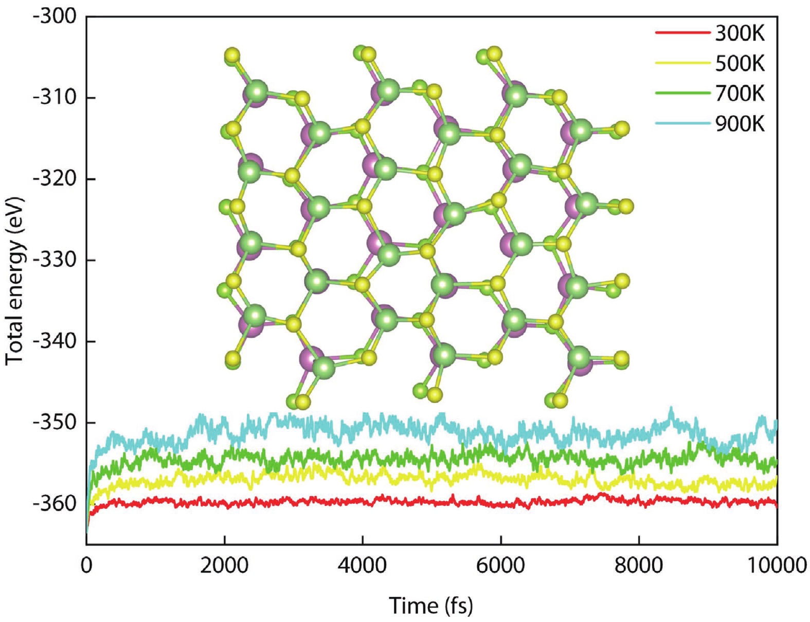
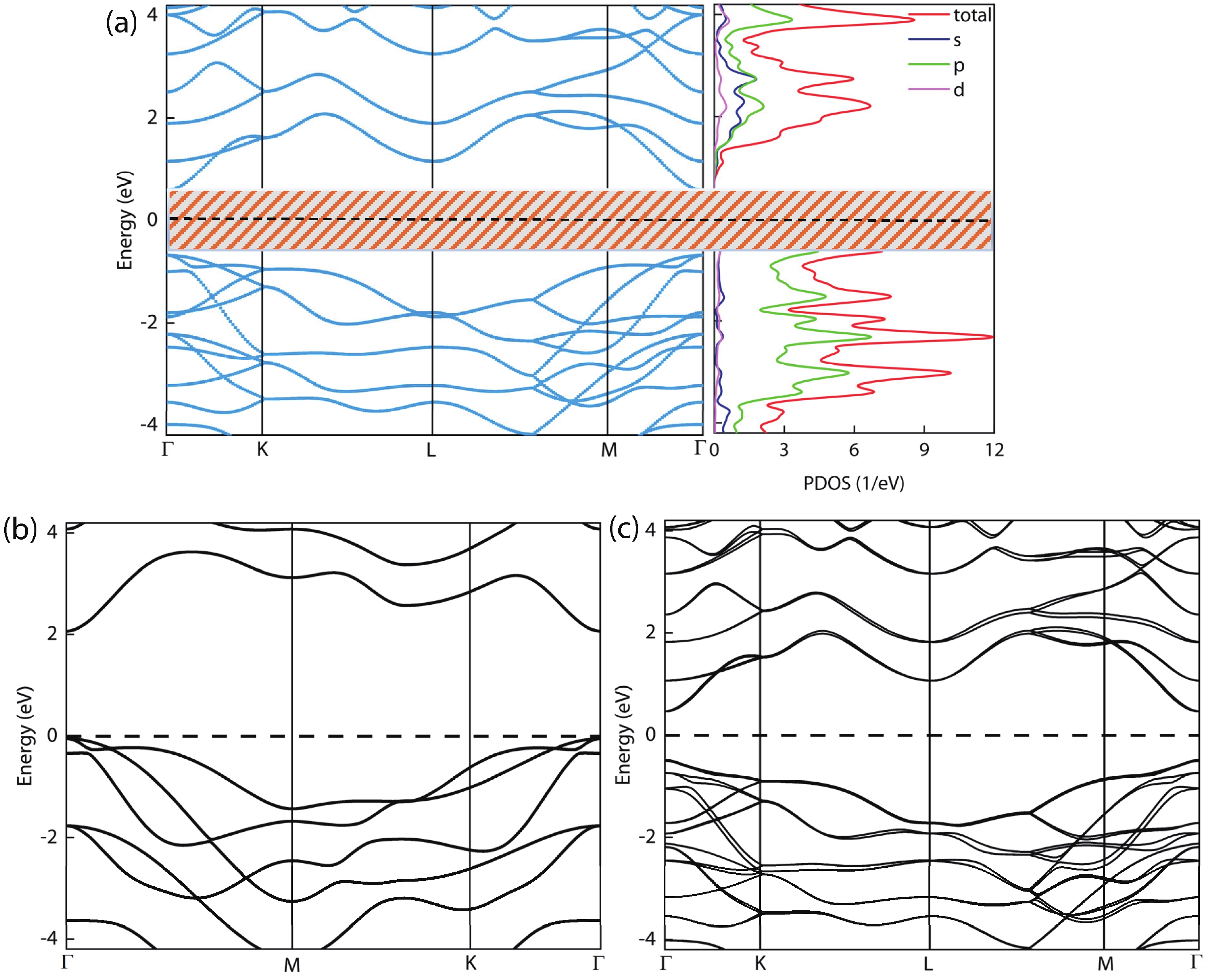
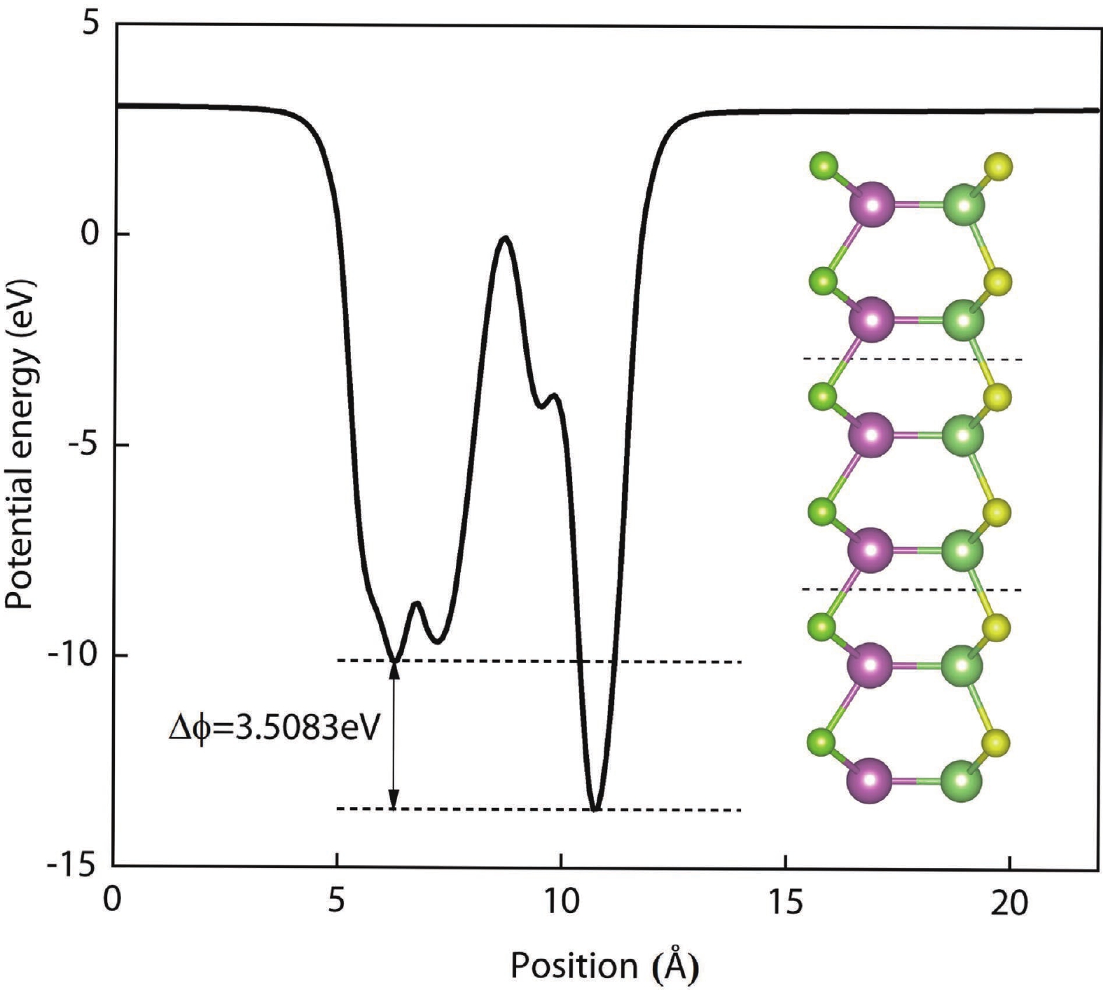
| [1] |
Zhang B T, Liu J, Yue S Z, et al. Hot electron injection: An efficacious approach to charge LaCoO 3 for improving the water splitting efficiency. Appl Catal B, 2017, 219, 432 doi: 10.1016/j.apcatb.2017.07.033 |
| [2] |
Wang W, Tade M O, Shao Z P. Research progress of perovskite materials in photocatalysis- and photovoltaics-related energy conversion and environmental treatment. Chem Soc Rev, 2015, 44, 5371 doi: 10.1039/C5CS00113G |
| [3] |
Ma M M, Huang Y B, Liu J, et al. Engineering the photoelectrochemical behaviors of ZnO for efficient solar water splitting. J Semicond, 2020, 41, 091702 doi: 10.1088/1674-4926/41/9/091702 |
| [4] |
Concina I, Ibupoto Z H, Vomiero A. Electrochemical water splitting: Semiconducting metal oxide nanostructures for water splitting and photovoltaics. Adv Energy Mater, 2017, 7, 1770138 doi: 10.1002/aenm.201770138 |
| [5] |
Zhao H, Dai Z Y, Xu X Y, et al. Integrating semiconducting catalyst of ReS 2 nanosheets into P-silicon photocathode for enhanced solar water reduction. ACS Appl Mater Interfaces, 2018, 10, 23074 doi: 10.1021/acsami.8b04740 |
| [6] |
Reece S Y, Hamel J A, Sung K, et al. Wireless solar water splitting using silicon-based semiconductors and earth-abundant catalysts. Science, 2011, 334, 645 doi: 10.1126/science.1209816 |
| [7] |
Novoselov K S, Geim A K, Morozov S V, et al. Electric field effect in atomically thin carbon films. Science, 2004, 306, 666 doi: 10.1126/science.1102896 |
| [8] |
Alyörük M M. Piezoelectric properties of monolayer II-VI group oxides by first-principles calculations. Phys Status Solidi B, 2016, 253, 2534 doi: 10.1002/pssb.201600387 |
| [9] |
Li X M, Zhang X, Park H, et al. Editorial: Electronics and optoelectronics of graphene and related 2D materials. Front Mater, 2020, 7, 235 doi: 10.3389/fmats.2020.00235 |
| [10] |
Liu B, Zhou K. Recent progress on graphene-analogous 2D nanomaterials: Properties, modeling and applications. Prog Mater Sci, 2019, 100, 99 doi: 10.1016/j.pmatsci.2018.09.004 |
| [11] |
Li C, Li J, Huang Y B, et al. Recent development in electronic structure tuning of graphitic carbon nitride for highly efficient photocatalysis. J Semicond, 2022, 43, 021701 doi: 10.1088/1674-4926/43/2/021701 |
| [12] |
Taghinejad H, Rehn D A, Muccianti C, et al. Defect-mediated alloying of monolayer transition-metal dichalcogenides. ACS Nano, 2018, 12, 12795 doi: 10.1021/acsnano.8b07920 |
| [13] |
Qiao M, Liu J, Wang Y, et al. PdSeO 3 monolayer: Promising inorganic 2D photocatalyst for direct overall water splitting without using sacrificial reagents and cocatalysts. J Am Chem Soc, 2018, 140, 12256 doi: 10.1021/jacs.8b07855 |
| [14] |
Sun Y H, Wang X J, Zhao X G, et al. First-principle high-throughput calculations of carrier effective masses of two-dimensional transition metal dichalcogenides. J Semicond, 2018, 39, 072001 doi: 10.1088/1674-4926/39/7/072001 |
| [15] |
Lu A Y, Zhu H Y, Xiao J, et al. Janus monolayers of transition metal dichalcogenides. Nat Nanotechnol, 2017, 12, 744 doi: 10.1038/nnano.2017.100 |
| [16] |
Zhang J, Jia S, Kholmanov I, et al. Janus monolayer transition-metal dichalcogenides. ACS Nano, 2017, 11, 8192 doi: 10.1021/acsnano.7b03186 |
| [17] |
Ju L, Bie M, Shang J, et al. Janus transition metal dichalcogenides: A superior platform for photocatalytic water splitting. J Phys Mater, 2020, 3, 022004 doi: 10.1088/2515-7639/ab7c57 |
| [18] |
Zhao P, Ma Y D, Lv X S, et al. Two-dimensional III 2-VI 3 materials: Promising photocatalysts for overall water splitting under infrared light spectrum. Nano Energy, 2018, 51, 533 doi: 10.1016/j.nanoen.2018.07.010 |
| [19] |
Zhou X F, Shen B, Lyubartsev A, et al. Semiconducting piezoelectric heterostructures for piezo- and piezophotocatalysis. Nano Energy, 2022, 96, 107141 doi: 10.1016/j.nanoen.2022.107141 |
| [20] |
Schneider J, Matsuoka M, Takeuchi M, et al. Understanding TiO 2 photocatalysis: Mechanisms and materials. Chem Rev, 2014, 114, 9919 doi: 10.1021/cr5001892 |
| [21] |
Liao G F, Gong Y, Zhang L, et al. Semiconductor polymeric graphitic carbon nitride photocatalysts: The “holy grail” for the photocatalytic hydrogen evolution reaction under visible light. Energy Environ Sci, 2019, 12, 2080 doi: 10.1039/C9EE00717B |
| [22] |
Wang P, Zong Y X, Liu H, et al. Highly efficient photocatalytic water splitting and enhanced piezoelectric properties of 2D Janus group-III chalcogenides. J Mater Chem C, 2021, 9, 4989 doi: 10.1039/D1TC00318F |
| [23] |
Rahaman R, Sharmin M, Podder J. Band gap tuning and p to n-type transition in Mn-doped CuO nanostructured thin films. J Semicond, 2022, 43, 012801 doi: 10.1088/1674-4926/43/1/012801 |
| [24] |
Yin Z, Hu M, Liu J, et al. Tunable crystal structure of Cu-Zn-Sn-S nanocrystals for improving photocatalytic hydrogen evolution enabled by copper element regulation. J Semicond, 2022, 43, 032701 doi: 10.1088/1674-4926/43/3/032701 |
| [25] |
Lee H J, Lee S W, Hwang H, et al. Vertically oriented MoS 2/WS 2 heterostructures on reduced graphene oxide sheets as electrocatalysts for hydrogen evolution reaction. Mater Chem Front, 2021, 5, 3396 doi: 10.1039/D1QM00051A |
| [26] |
Wang S K, Ren C D, Tian H Y, et al. MoS 2/ZnO van der Waals heterostructure as a high-efficiency water splitting photocatalyst: A first-principles study. Phys Chem Chem Phys, 2018, 20, 13394 doi: 10.1039/C8CP00808F |
| [27] |
Dang C Q, Lu A L, Wang H Y, et al. Diamond semiconductor and elastic strain engineering. J Semicond, 2022, 43, 021801 doi: 10.1088/1674-4926/43/2/021801 |
| [28] |
Thulin L, Guerra J. Calculations of strain-modified anatase TiO 2 band structures. Phys Rev B, 2008, 77, 195112 doi: 10.1103/PhysRevB.77.195112 |
| [29] |
Gao Q, Sahin H, Kang J. Strain tunable band structure of a new 2D carbon allotrope C 568. J Semicond, 2020, 41, 082005 doi: 10.1088/1674-4926/41/8/082005 |
| [30] |
Giannozzi P, Baroni S, Bonini N, et al. QUANTUM ESPRESSO: A modular and open-source software project for quantum simulations of materials. J Phys: Condens Matter, 2009, 21, 395502 doi: 10.1088/0953-8984/21/39/395502 |
| [31] |
Giannozzi P, Andreussi O, Brumme T, et al. Advanced capabilities for materials modelling with QUANTUM ESPRESSO. J Phys: Condens Matter, 2017, 29, 465901 doi: 10.1088/1361-648X/aa8f79 |
| [32] |
Heyd J, Scuseria G E, Ernzerhof M. Hybrid functionals based on a screened Coulomb potential. J Chem Phys, 2003, 118, 8207 doi: 10.1063/1.1564060 |
| [33] |
Heyd J, Scuseria G E, Ernzerhof M. Erratum: "Hybrid functionals based on a screened Coulomb potential" [J. Chem. Phys. 118, 8207 (2003)]. J Chem Phys, 2006, 124, 219906 doi: 10.1063/1.2204597 |
| [34] |
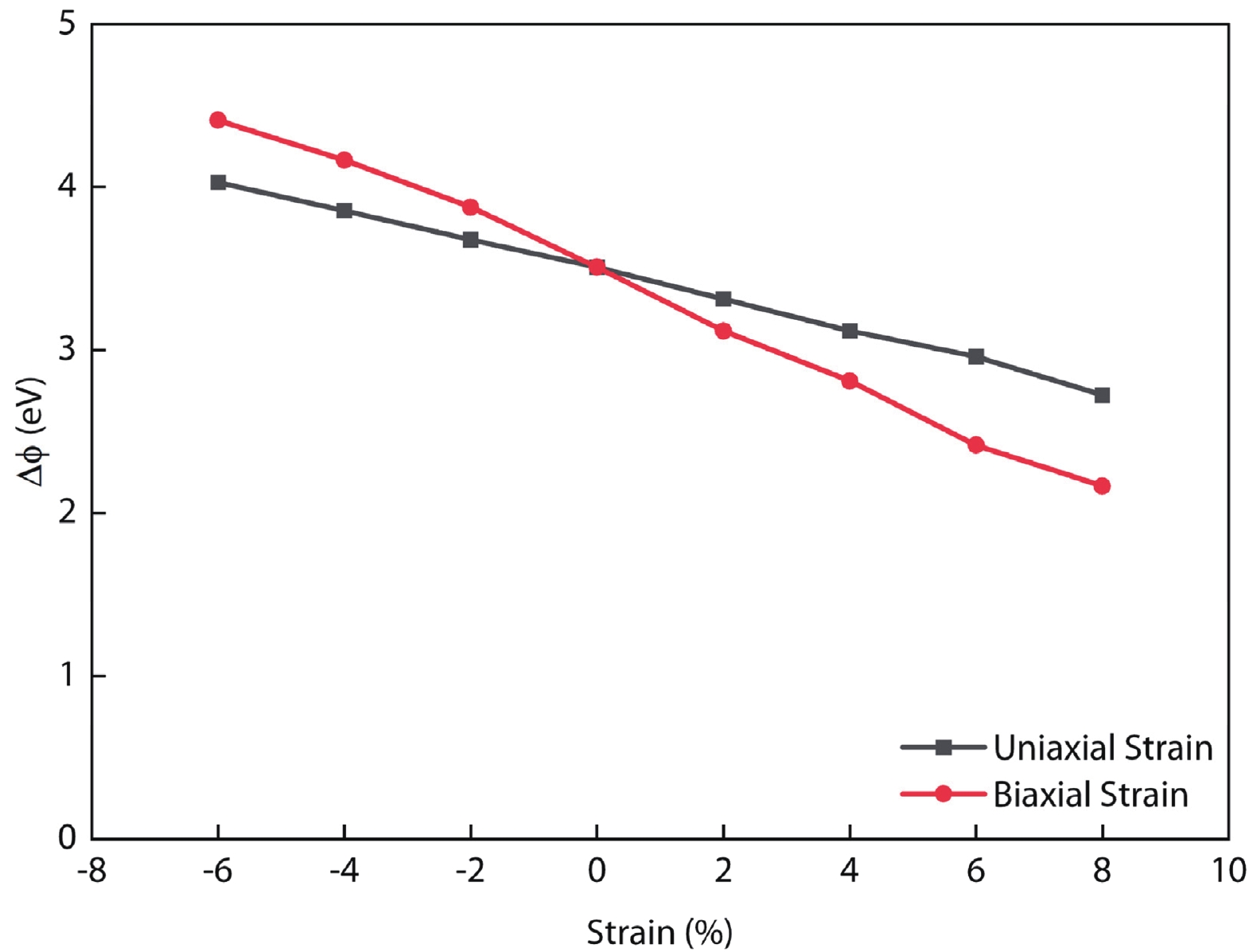
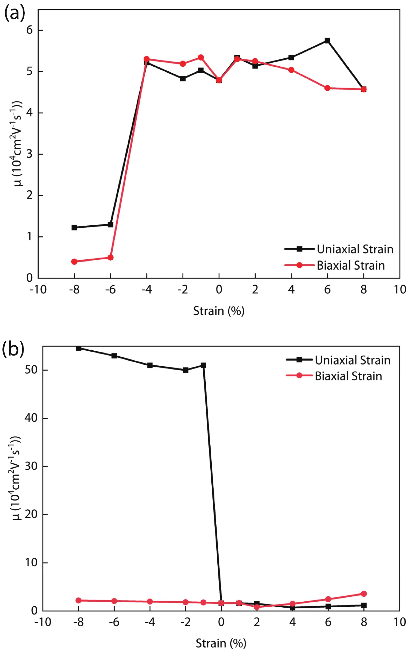
|
| [35] |
Guo S D. Phonon transport in Janus monolayer MoSSe: A first-principles study. Phys Chem Chem Phys, 2018, 20, 7236 doi: 10.1039/C8CP00350E |
| [36] |
Dong L, Lou J, Shenoy V B. Large In-plane and vertical piezoelectricity in Janus transition metal dichalchogenides. ACS Nano, 2017, 11, 8242 doi: 10.1021/acsnano.7b03313 |
| [37] |
|
| [38] |
Born M, Huang K. Dynamical theory of crystal lattices. Oxford: Clarendon Press, 1954
|
| [39] |
Peng R, Ma Y D, Huang B B, et al. Two-dimensional Janus PtSSe for photocatalytic water splitting under the visible or infrared light. J Mater Chem A, 2019, 7, 603 doi: 10.1039/C8TA09177C |
| [40] |
Kaasbjerg K, Thygesen K S, Jauho A P. Acoustic phonon limited mobility in two-dimensional semiconductors: Deformation potential and piezoelectric scattering in monolayer MoS 2 from first principles. Phys Rev B, 2013, 87, 235312 doi: 10.1103/PhysRevB.87.235312 |
| [41] |
Xi J Y, Long M Q, Tang L, et al. First-principles prediction of charge mobility in carbon and organic nanomaterials. Nanoscale, 2012, 4, 4348 doi: 10.1039/c2nr30585b |
| [42] |
Yin W J, Wen B, Nie G Z, et al. Tunable dipole and carrier mobility for a few layer Janus MoSSe structure. J Mater Chem C, 2018, 6, 1693 doi: 10.1039/C7TC05225A |
| [43] |
Zhang Y Z, Ye H, Yu Z Y, et al. First-principles study of square phase MX2 and Janus $MX\varUpsilon $ ( M = Mo, W; $X $, $\varUpsilon $ = S, Se, Te) transition metal dichalcogenide monolayers under biaxial strain. Phys E, 2019, 110, 134 doi: 10.1016/j.physe.2019.02.009 |
| [44] |
Chaves A, Azadani J G, Alsalman H, et al. Bandgap engineering of two-dimensional semiconductor materials. npj 2D Mater Appl, 2020, 4, 1 doi: 10.1038/s41699-019-0135-1 |


 DownLoad:


 Li Zhong:received his BE degree in 2021 from Department of Engineering Mechanics, Hefei University of Technology. Currently he is a master student in Hefei University of Technology. His research interest includes mech-electrochemistry coupling behaviors, energy-related topics in nanomaterials and photocatalytic water splitting
 Xiaobao Li:received his BE degree in 2008 from Department of Chemical Engineering and Technology, Hefei University of Technology and PhD degree in 2016 from Mechanical Engineering Department, University of Houston. Currently he is a professor in Department of Engineering Mechanics, Hefei University of Technology. His research interest includes electromechanical coupling, mech-electrochemistry coupling behaviors and energy-related topics in nanomaterials
 Xinle Xiao:received his PhD degree from University of Science and Technology of China in 2020. Now he is an associate professor in Chizhou University. His research includes development and performance optimization of fuel cell membranes, preparation of divalent ion separation membranes, and membrane process simulation


