


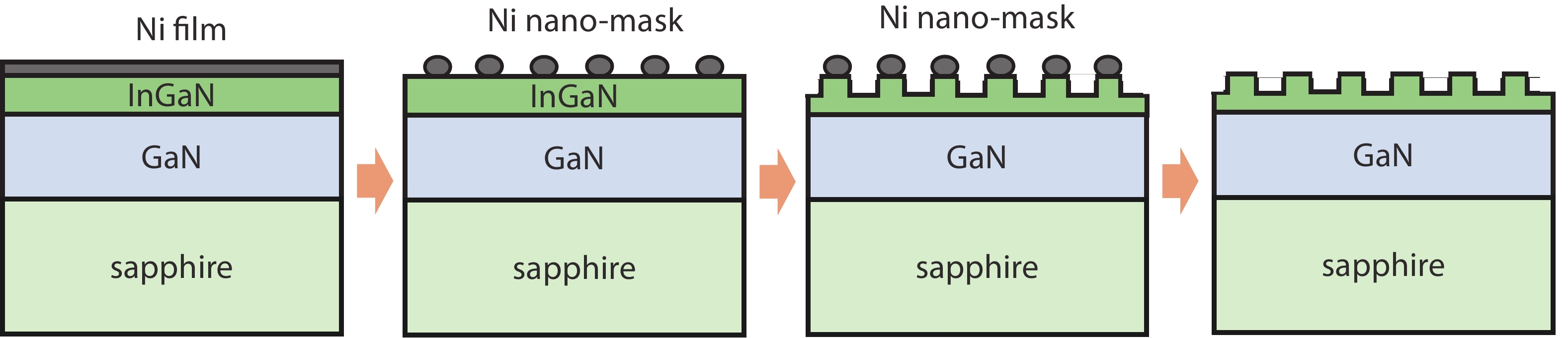
Fig. 1.
(Color online) Schematic representation of the process of preparing a nano-patterned InGaN layer by self-assembled Ni nano-masks.
ARTICLES
Ruoshi Peng, Shengrui Xu, Xiaomeng Fan, Hongchang Tao, Huake Su, Yuan Gao, Jincheng Zhang and Yue Hao
Corresponding author: Shengrui Xu, shengruixidian@126.com; Jincheng Zhang, jchzhang@xidian.edu.cn
Abstract: The nano-patterned InGaN film was used in green InGaN/GaN multiple quantum wells (MQWs) structure, to relieve the unpleasantly existing mismatch between high indium content InGaN and GaN, as well as to enhance the light output. The different self-assembled nano-masks were formed on InGaN by annealing thin Ni layers of different thicknesses. Whereafter, the InGaN films were etched into nano-patterned films. Compared with the green MQWs structure grown on untreated InGaN film, which on nano-patterned InGaN had better luminous performance. Among them the MQWs performed best when 3 nm thick Ni film was used as mask, because that optimally balanced the effects of nano-patterned InGaN on the crystal quality and the light output.
Keywords: GaN, InGaN, nano-mask, nano-patterned, MQWs
| [1] |
Nakamura S, Mukai T, Senoh M. Candela-class high-brightness InGaN/AlGaN double-heterostructure blue-light-emitting diodes. Appl Phys Lett, 1994, 64, 1687 doi: 10.1063/1.111832
|
| [2] |
Saito S, Hashimoto R, Hwang J, et al. InGaN light-emitting diodes on c-face sapphire substrates in green gap spectral range. Appl Phys Express, 2013, 6, 111004 doi: 10.7567/APEX.6.111004
|
| [3] |
Langer T, Kruse A, Ketzer F A, et al. Origin of the “green gap”: Increasing nonradiative recombination in indium-rich GaInN/GaN quantum well structures. Phys Status Solidi C, 2011, 8, 2170 doi: 10.1002/pssc.201001051
|
| [4] |
Kong J, Feng M X, Cai J, et al. GaN grown on nano-patterned sapphire substrates. J Semicond, 2015, 36, 043003 doi: 10.1088/1674-4926/36/4/043003
|
| [5] |
Yamaguchi S, Kariya M, Nitta S, et al. Structural properties of InN on GaN grown by metalorganic vapor-phase epitaxy. J Appl Phys, 1999, 85, 7682 doi: 10.1063/1.370571
|
| [6] |
Ho I H, Stringfellow G B. Solid phase immiscibility in GaInN. Appl Phys Lett, 1996, 69, 2701 doi: 10.1063/1.117683
|
| [7] |
Albrecht M, Strunk H P, Weyher J L, et al. Carrier recombination at single dislocations in GaN measured by cathodoluminescence in a transmission electron microscope. J Appl Phys, 2002, 92, 2000 doi: 10.1063/1.1490618
|
| [8] |
Huh C, Lee K S, Kang E J, et al. Improved light-output and electrical performance of InGaN-based light-emitting diode by microroughening of the p-GaN surface. J Appl Phys, 2003, 93, 9383 doi: 10.1063/1.1571962
|
| [9] |
Niu N H, Wang H B, Liu J P, et al. Improved quality of InGaN/GaN multiple quantum wells by a strain relief layer. J Cryst Growth, 2006, 286, 209 doi: 10.1016/j.jcrysgro.2005.09.027
|
| [10] |
Wang J X, Wang L, Zhao W, et al. Study on internal quantum efficiency of blue InGaN multiple-quantum-well with an InGaN underneath layer. Sci China Technol Sci, 2010, 53, 306 doi: 10.1007/s11431-010-0062-z
|
| [11] |
Akasaka T, Gotoh H, Kobayashi Y, et al. InGaN quantum wells with small potential fluctuation grown on InGaN underlying layers. Appl Phys Lett, 2006, 89, 101110 doi: 10.1063/1.2347115
|
| [12] |
Wang J X, Wang L, Zhao W, et al. Understanding efficiency droop effect in InGaN/GaN multiple-quantum-well blue light-emitting diodes with different degree of carrier localization. Appl Phys Lett, 2010, 97, 201112 doi: 10.1063/1.3520139
|
| [13] |
Lin R M, Lu Y C, Yu S F, et al. Enhanced extraction and efficiency of blue light-emitting diodes prepared using two-step-etched patterned sapphire substrates. J Electrochem Soc, 2009, 156, H874 doi: 10.1149/1.3231502
|
| [14] |
Kim J Y, Kwon M K, Kim J P, et al. Enhanced light extraction from triangular GaN-based light-emitting diodes. IEEE Photonics Technol Lett, 2007, 19, 1865 doi: 10.1109/LPT.2007.907644
|
| [15] |
Du J J, Xu S R, Peng R S, et al. Enhancement of optical characteristic of InGaN/GaN multiple quantum-well structures by self-growing air voids. Sci China Technol Sci, 2021, 64, 1583 doi: 10.1007/s11431-021-1868-7
|
| [16] |
Fujii T, Gao Y, Sharma R, et al. Increase in the extraction efficiency of GaN-based light-emitting diodes via surface roughening. Appl Phys Lett, 2004, 84, 855 doi: 10.1063/1.1645992
|
| [17] |
Wang R J, Liu D, Zuo Z Y, et al. Metal-assisted electroless fabrication of nanoporous p-GaN for increasing the light extraction efficiency of light emitting diodes. AIP Adv, 2012, 2, 012109 doi: 10.1063/1.3679150
|
| [18] |
Tao H C, Xu S R, Mao W, et al. Improved crystal quality of nonpolar a-plane GaN based on the nano pattern formed by the annealed thin Ni layer. Superlattices Microstruct, 2019, 130, 539 doi: 10.1016/j.spmi.2019.05.020
|
| [19] |
Carey J D, Ong L L, Silva S P. Formation of low-temperature self-organized nanoscale nickel metal Islands. Nanotechnology, 2003, 14, 1223 doi: 10.1088/0957-4484/14/11/011
|
| [20] |
Chiu C H, Lo M H, Lu T C, et al. Nano-processing techniques applied in GaN-based light-emitting devices with self-assembly Ni nano-masks. J Lightwave Technol, 2008, 26, 1445 doi: 10.1109/JLT.2008.922157
|
| [21] |
Moram M A, Vickers M E. X-ray diffraction of III-nitrides. Rep Prog Phys, 2009, 72, 036502 doi: 10.1088/0034-4885/72/3/036502
|
| [22] |
Ashby C I H, Mitchell C C, Han J, et al. Low-dislocation-density GaN from a single growth on a textured substrate. Appl Phys Lett, 2000, 77, 3233 doi: 10.1063/1.1325394
|
| [23] |
He C G, Zhao W, Zhang K, et al. High-quality GaN epilayers achieved by facet-controlled epitaxial lateral overgrowth on sputtered AlN/PSS templates. ACS Appl Mater Interfaces, 2017, 9, 43386 doi: 10.1021/acsami.7b14801
|
| [24] |
Oh M S, Kwon M K, Park I K, et al. Improvement of green LED by growing p-GaN on In0.25GaN/GaN MQWs at low temperature. J Cryst Growth, 2006, 289, 107 doi: 10.1016/j.jcrysgro.2005.10.129
|
| [25] |
Schnitzer I, Yablonovitch E, Caneau C, et al. 30% external quantum efficiency from surface textured, thin-film light-emitting diodes. Appl Phys Lett, 1993, 63, 2174 doi: 10.1063/1.110575
|
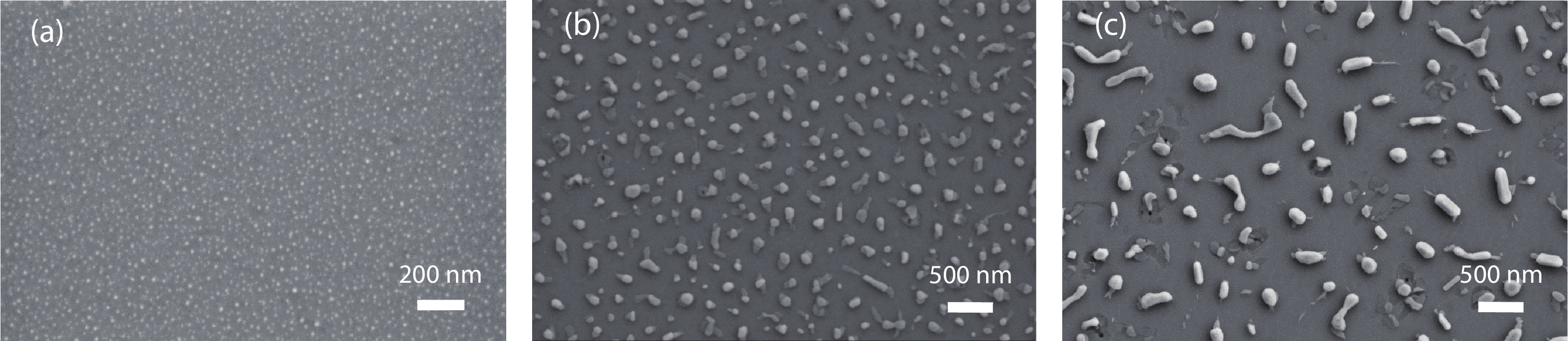
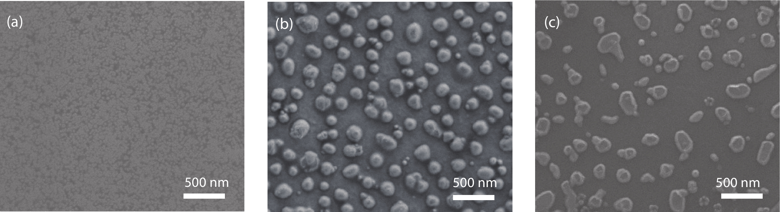
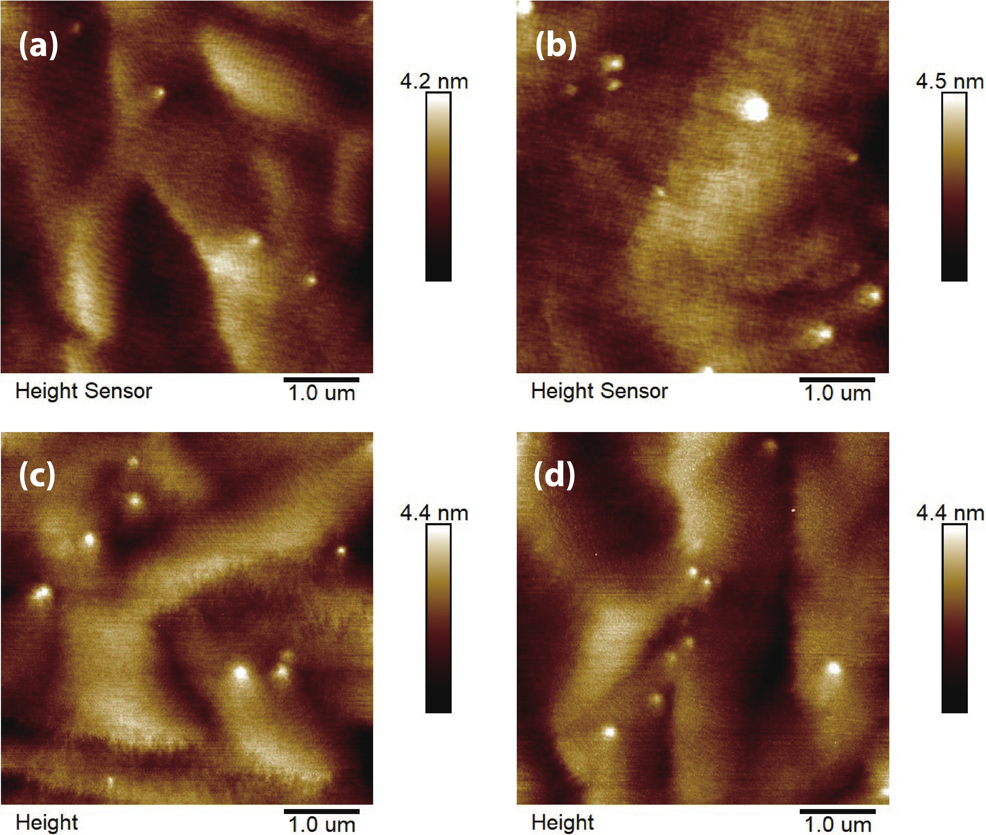
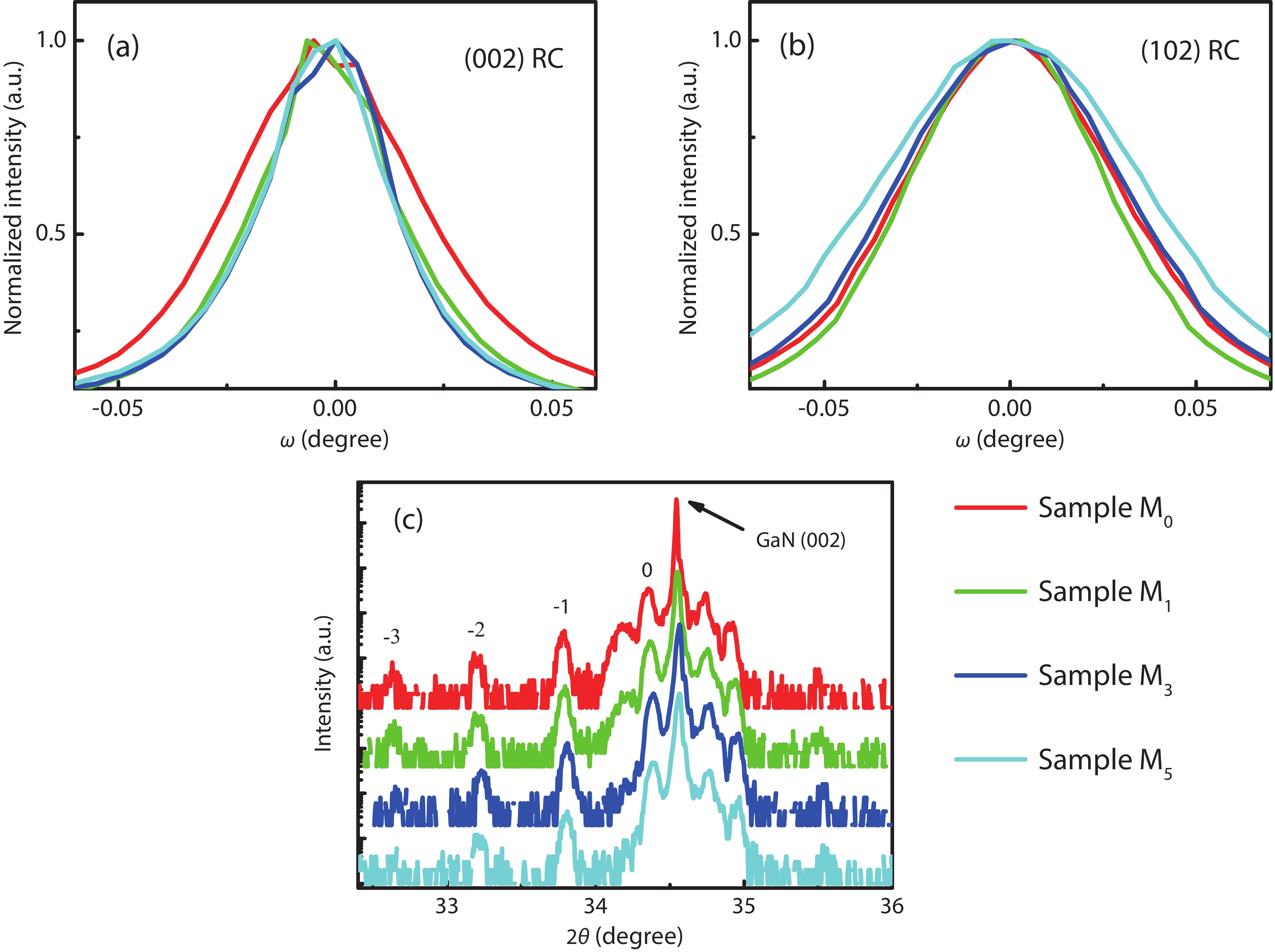
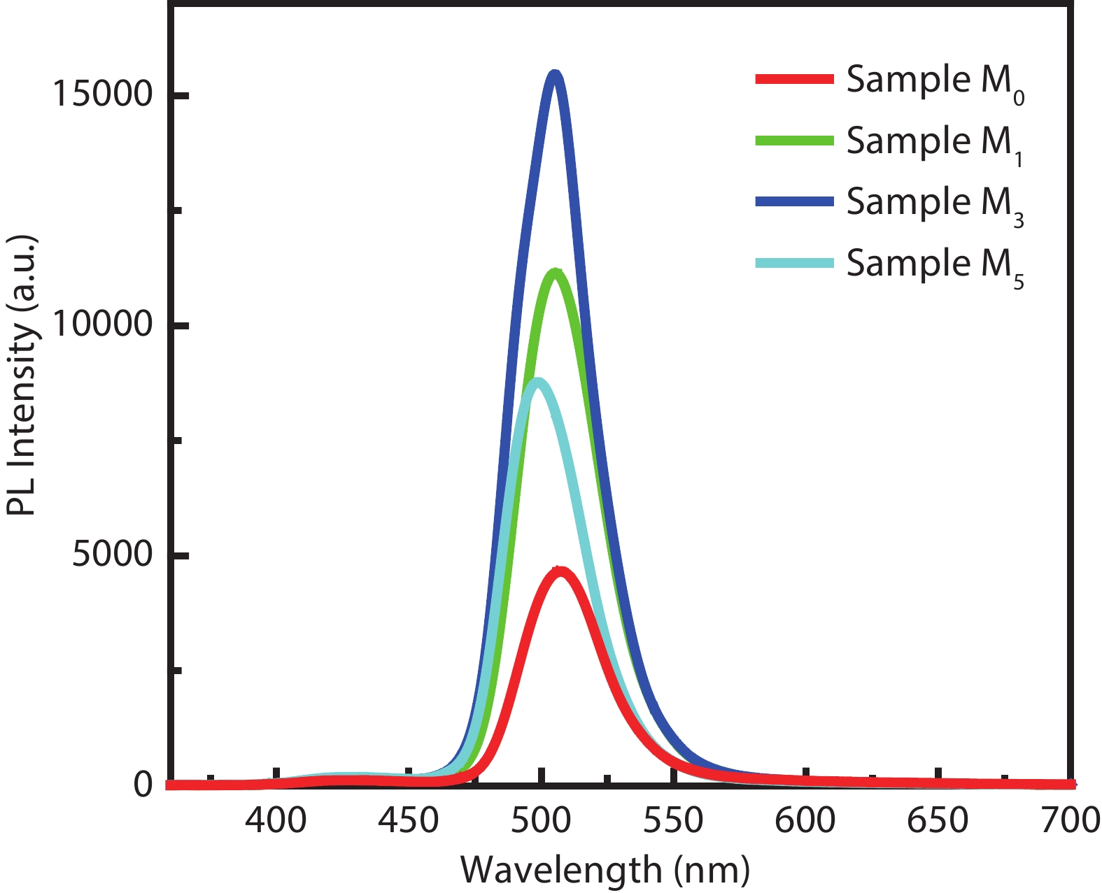
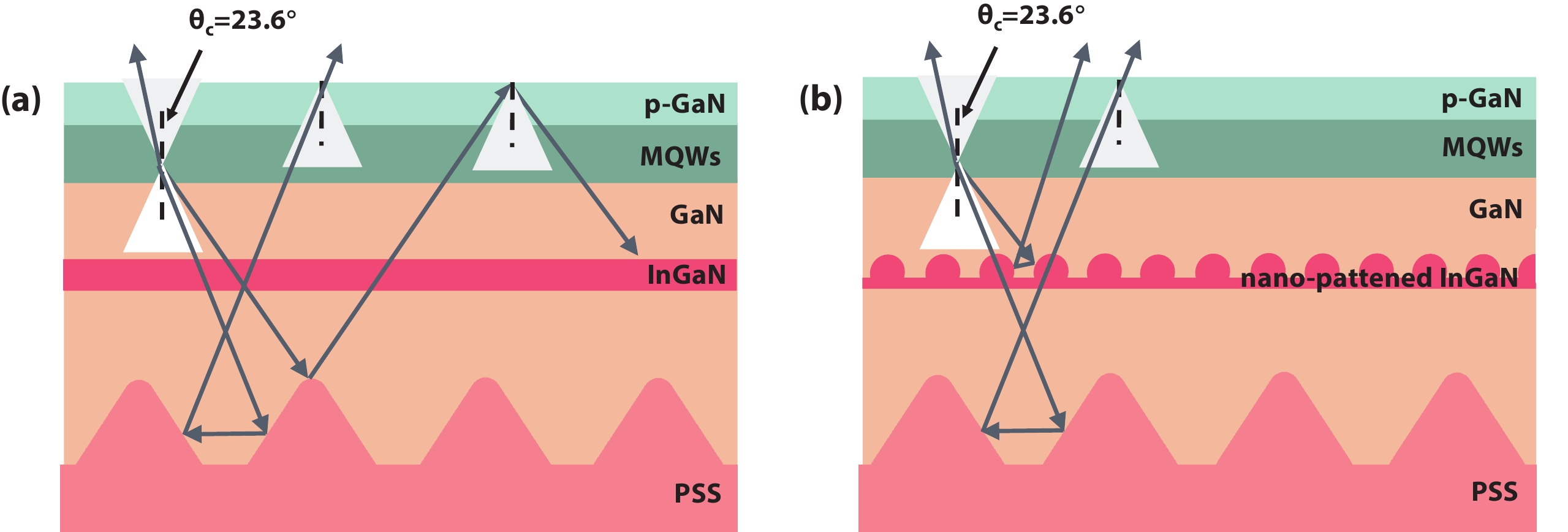
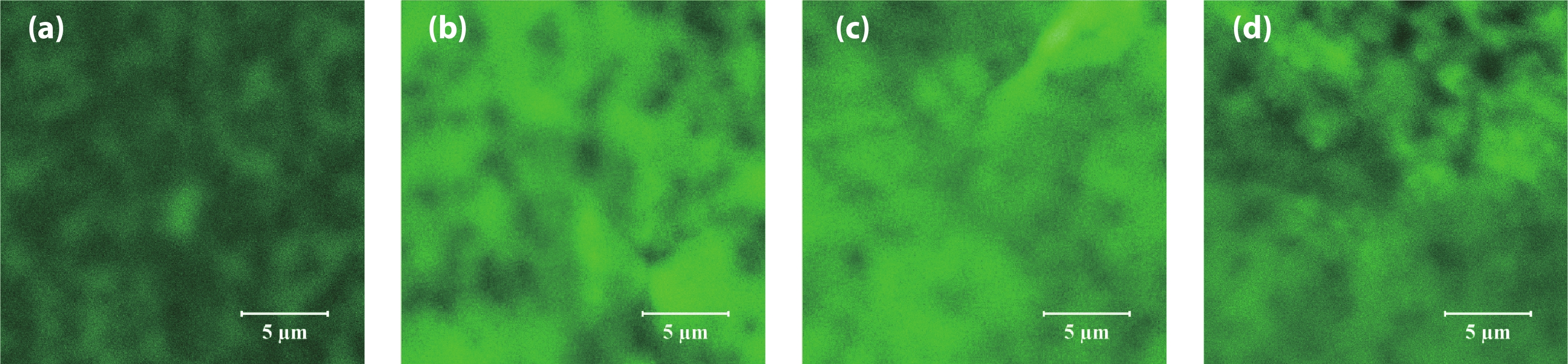
Table 1. The XRD FWHM of GaN at (002) and (102) plane and the dislocation density of samples.
| Parameter | Sample M0 | Sample M1 | Sample M3 | Sample M5 |
| FWHM of (002) (arcsec) | 191.0 | 142.3 | 131.5 | 132.8 |
| FWHM of (102) (arcsec) | 261.8 | 239.8 | 276.2 | 326.8 |
| Dislocation density (108 cm−2) | 4.36 | 3.45 | 4.39 | 6.01 |
 DownLoad: CSV
| [1] |
Nakamura S, Mukai T, Senoh M. Candela-class high-brightness InGaN/AlGaN double-heterostructure blue-light-emitting diodes. Appl Phys Lett, 1994, 64, 1687 doi: 10.1063/1.111832
|
| [2] |
Saito S, Hashimoto R, Hwang J, et al. InGaN light-emitting diodes on c-face sapphire substrates in green gap spectral range. Appl Phys Express, 2013, 6, 111004 doi: 10.7567/APEX.6.111004
|
| [3] |
Langer T, Kruse A, Ketzer F A, et al. Origin of the “green gap”: Increasing nonradiative recombination in indium-rich GaInN/GaN quantum well structures. Phys Status Solidi C, 2011, 8, 2170 doi: 10.1002/pssc.201001051
|
| [4] |
Kong J, Feng M X, Cai J, et al. GaN grown on nano-patterned sapphire substrates. J Semicond, 2015, 36, 043003 doi: 10.1088/1674-4926/36/4/043003
|
| [5] |
Yamaguchi S, Kariya M, Nitta S, et al. Structural properties of InN on GaN grown by metalorganic vapor-phase epitaxy. J Appl Phys, 1999, 85, 7682 doi: 10.1063/1.370571
|
| [6] |
Ho I H, Stringfellow G B. Solid phase immiscibility in GaInN. Appl Phys Lett, 1996, 69, 2701 doi: 10.1063/1.117683
|
| [7] |
Albrecht M, Strunk H P, Weyher J L, et al. Carrier recombination at single dislocations in GaN measured by cathodoluminescence in a transmission electron microscope. J Appl Phys, 2002, 92, 2000 doi: 10.1063/1.1490618
|
| [8] |
Huh C, Lee K S, Kang E J, et al. Improved light-output and electrical performance of InGaN-based light-emitting diode by microroughening of the p-GaN surface. J Appl Phys, 2003, 93, 9383 doi: 10.1063/1.1571962
|
| [9] |
Niu N H, Wang H B, Liu J P, et al. Improved quality of InGaN/GaN multiple quantum wells by a strain relief layer. J Cryst Growth, 2006, 286, 209 doi: 10.1016/j.jcrysgro.2005.09.027
|
| [10] |
Wang J X, Wang L, Zhao W, et al. Study on internal quantum efficiency of blue InGaN multiple-quantum-well with an InGaN underneath layer. Sci China Technol Sci, 2010, 53, 306 doi: 10.1007/s11431-010-0062-z
|
| [11] |
Akasaka T, Gotoh H, Kobayashi Y, et al. InGaN quantum wells with small potential fluctuation grown on InGaN underlying layers. Appl Phys Lett, 2006, 89, 101110 doi: 10.1063/1.2347115
|
| [12] |
Wang J X, Wang L, Zhao W, et al. Understanding efficiency droop effect in InGaN/GaN multiple-quantum-well blue light-emitting diodes with different degree of carrier localization. Appl Phys Lett, 2010, 97, 201112 doi: 10.1063/1.3520139
|
| [13] |
Lin R M, Lu Y C, Yu S F, et al. Enhanced extraction and efficiency of blue light-emitting diodes prepared using two-step-etched patterned sapphire substrates. J Electrochem Soc, 2009, 156, H874 doi: 10.1149/1.3231502
|
| [14] |
Kim J Y, Kwon M K, Kim J P, et al. Enhanced light extraction from triangular GaN-based light-emitting diodes. IEEE Photonics Technol Lett, 2007, 19, 1865 doi: 10.1109/LPT.2007.907644
|
| [15] |
Du J J, Xu S R, Peng R S, et al. Enhancement of optical characteristic of InGaN/GaN multiple quantum-well structures by self-growing air voids. Sci China Technol Sci, 2021, 64, 1583 doi: 10.1007/s11431-021-1868-7
|
| [16] |
Fujii T, Gao Y, Sharma R, et al. Increase in the extraction efficiency of GaN-based light-emitting diodes via surface roughening. Appl Phys Lett, 2004, 84, 855 doi: 10.1063/1.1645992
|
| [17] |
Wang R J, Liu D, Zuo Z Y, et al. Metal-assisted electroless fabrication of nanoporous p-GaN for increasing the light extraction efficiency of light emitting diodes. AIP Adv, 2012, 2, 012109 doi: 10.1063/1.3679150
|
| [18] |
Tao H C, Xu S R, Mao W, et al. Improved crystal quality of nonpolar a-plane GaN based on the nano pattern formed by the annealed thin Ni layer. Superlattices Microstruct, 2019, 130, 539 doi: 10.1016/j.spmi.2019.05.020
|
| [19] |
Carey J D, Ong L L, Silva S P. Formation of low-temperature self-organized nanoscale nickel metal Islands. Nanotechnology, 2003, 14, 1223 doi: 10.1088/0957-4484/14/11/011
|
| [20] |
Chiu C H, Lo M H, Lu T C, et al. Nano-processing techniques applied in GaN-based light-emitting devices with self-assembly Ni nano-masks. J Lightwave Technol, 2008, 26, 1445 doi: 10.1109/JLT.2008.922157
|
| [21] |
Moram M A, Vickers M E. X-ray diffraction of III-nitrides. Rep Prog Phys, 2009, 72, 036502 doi: 10.1088/0034-4885/72/3/036502
|
| [22] |
Ashby C I H, Mitchell C C, Han J, et al. Low-dislocation-density GaN from a single growth on a textured substrate. Appl Phys Lett, 2000, 77, 3233 doi: 10.1063/1.1325394
|
| [23] |
He C G, Zhao W, Zhang K, et al. High-quality GaN epilayers achieved by facet-controlled epitaxial lateral overgrowth on sputtered AlN/PSS templates. ACS Appl Mater Interfaces, 2017, 9, 43386 doi: 10.1021/acsami.7b14801
|
| [24] |
Oh M S, Kwon M K, Park I K, et al. Improvement of green LED by growing p-GaN on In0.25GaN/GaN MQWs at low temperature. J Cryst Growth, 2006, 289, 107 doi: 10.1016/j.jcrysgro.2005.10.129
|
| [25] |
Schnitzer I, Yablonovitch E, Caneau C, et al. 30% external quantum efficiency from surface textured, thin-film light-emitting diodes. Appl Phys Lett, 1993, 63, 2174 doi: 10.1063/1.110575
|


Article views: 1635 Times PDF downloads: 102 Times Cited by: 0 Times
Received: 27 September 2022 Revised: 29 November 2022 Online: Uncorrected proof: 10 January 2023Accepted Manuscript: 10 January 2023Published: 10 April 2023
| Citation: |
Ruoshi Peng, Shengrui Xu, Xiaomeng Fan, Hongchang Tao, Huake Su, Yuan Gao, Jincheng Zhang, Yue Hao. Application of nano-patterned InGaN fabricated by self-assembled Ni nano-masks in green InGaN/GaN multiple quantum wells[J]. Journal of Semiconductors, 2023, 44(4): 042801. doi: 10.1088/1674-4926/44/4/042801
****
R S Peng, S R Xu, X M Fan, H C Tao, H K Su, Y Gao, J C Zhang, Y Hao. Application of nano-patterned InGaN fabricated by self-assembled Ni nano-masks in green InGaN/GaN multiple quantum wells[J]. J. Semicond, 2023, 44(4): 042801. doi: 10.1088/1674-4926/44/4/042801

|
 Ruoshi Peng:received the B.Eng. degree from Xidian University, Xi’an, China, in 2016. She is currently pursuing the Ph.D. degree with the School of Microelectronics, Xidian University. Her current research interest is the GaN-based optoelectronic devices
 Shengrui Xu:received the B.S. and Ph.D. degrees from Xidian University, Xi’an, China, in 2005 and 2010, respectively. He is currently a Professor with the School of Microelectronics, Xidian University. His current research interests include GaN-based optoelectronic devices and wide gap-band materials and devices
 Jincheng Zhang:received the M.S. and Ph.D. degrees from Xidian University, Xi’an, China, in 2001 and 2004, respectively. He is currently a Professor with Xidian University. His current research interests include wide gap-band semiconductor GaN and diamond materials and devices
| [1] |
Nakamura S, Mukai T, Senoh M. Candela-class high-brightness InGaN/AlGaN double-heterostructure blue-light-emitting diodes. Appl Phys Lett, 1994, 64, 1687 doi: 10.1063/1.111832
|
| [2] |
Saito S, Hashimoto R, Hwang J, et al. InGaN light-emitting diodes on c-face sapphire substrates in green gap spectral range. Appl Phys Express, 2013, 6, 111004 doi: 10.7567/APEX.6.111004
|
| [3] |
Langer T, Kruse A, Ketzer F A, et al. Origin of the “green gap”: Increasing nonradiative recombination in indium-rich GaInN/GaN quantum well structures. Phys Status Solidi C, 2011, 8, 2170 doi: 10.1002/pssc.201001051
|
| [4] |
Kong J, Feng M X, Cai J, et al. GaN grown on nano-patterned sapphire substrates. J Semicond, 2015, 36, 043003 doi: 10.1088/1674-4926/36/4/043003
|
| [5] |
Yamaguchi S, Kariya M, Nitta S, et al. Structural properties of InN on GaN grown by metalorganic vapor-phase epitaxy. J Appl Phys, 1999, 85, 7682 doi: 10.1063/1.370571
|
| [6] |
Ho I H, Stringfellow G B. Solid phase immiscibility in GaInN. Appl Phys Lett, 1996, 69, 2701 doi: 10.1063/1.117683
|
| [7] |
Albrecht M, Strunk H P, Weyher J L, et al. Carrier recombination at single dislocations in GaN measured by cathodoluminescence in a transmission electron microscope. J Appl Phys, 2002, 92, 2000 doi: 10.1063/1.1490618
|
| [8] |
Huh C, Lee K S, Kang E J, et al. Improved light-output and electrical performance of InGaN-based light-emitting diode by microroughening of the p-GaN surface. J Appl Phys, 2003, 93, 9383 doi: 10.1063/1.1571962
|
| [9] |
Niu N H, Wang H B, Liu J P, et al. Improved quality of InGaN/GaN multiple quantum wells by a strain relief layer. J Cryst Growth, 2006, 286, 209 doi: 10.1016/j.jcrysgro.2005.09.027
|
| [10] |
Wang J X, Wang L, Zhao W, et al. Study on internal quantum efficiency of blue InGaN multiple-quantum-well with an InGaN underneath layer. Sci China Technol Sci, 2010, 53, 306 doi: 10.1007/s11431-010-0062-z
|
| [11] |
Akasaka T, Gotoh H, Kobayashi Y, et al. InGaN quantum wells with small potential fluctuation grown on InGaN underlying layers. Appl Phys Lett, 2006, 89, 101110 doi: 10.1063/1.2347115
|
| [12] |
Wang J X, Wang L, Zhao W, et al. Understanding efficiency droop effect in InGaN/GaN multiple-quantum-well blue light-emitting diodes with different degree of carrier localization. Appl Phys Lett, 2010, 97, 201112 doi: 10.1063/1.3520139
|
| [13] |
Lin R M, Lu Y C, Yu S F, et al. Enhanced extraction and efficiency of blue light-emitting diodes prepared using two-step-etched patterned sapphire substrates. J Electrochem Soc, 2009, 156, H874 doi: 10.1149/1.3231502
|
| [14] |
Kim J Y, Kwon M K, Kim J P, et al. Enhanced light extraction from triangular GaN-based light-emitting diodes. IEEE Photonics Technol Lett, 2007, 19, 1865 doi: 10.1109/LPT.2007.907644
|
| [15] |
Du J J, Xu S R, Peng R S, et al. Enhancement of optical characteristic of InGaN/GaN multiple quantum-well structures by self-growing air voids. Sci China Technol Sci, 2021, 64, 1583 doi: 10.1007/s11431-021-1868-7
|
| [16] |
Fujii T, Gao Y, Sharma R, et al. Increase in the extraction efficiency of GaN-based light-emitting diodes via surface roughening. Appl Phys Lett, 2004, 84, 855 doi: 10.1063/1.1645992
|
| [17] |
Wang R J, Liu D, Zuo Z Y, et al. Metal-assisted electroless fabrication of nanoporous p-GaN for increasing the light extraction efficiency of light emitting diodes. AIP Adv, 2012, 2, 012109 doi: 10.1063/1.3679150
|
| [18] |
Tao H C, Xu S R, Mao W, et al. Improved crystal quality of nonpolar a-plane GaN based on the nano pattern formed by the annealed thin Ni layer. Superlattices Microstruct, 2019, 130, 539 doi: 10.1016/j.spmi.2019.05.020
|
| [19] |
Carey J D, Ong L L, Silva S P. Formation of low-temperature self-organized nanoscale nickel metal Islands. Nanotechnology, 2003, 14, 1223 doi: 10.1088/0957-4484/14/11/011
|
| [20] |
Chiu C H, Lo M H, Lu T C, et al. Nano-processing techniques applied in GaN-based light-emitting devices with self-assembly Ni nano-masks. J Lightwave Technol, 2008, 26, 1445 doi: 10.1109/JLT.2008.922157
|
| [21] |
Moram M A, Vickers M E. X-ray diffraction of III-nitrides. Rep Prog Phys, 2009, 72, 036502 doi: 10.1088/0034-4885/72/3/036502
|
| [22] |
Ashby C I H, Mitchell C C, Han J, et al. Low-dislocation-density GaN from a single growth on a textured substrate. Appl Phys Lett, 2000, 77, 3233 doi: 10.1063/1.1325394
|
| [23] |
He C G, Zhao W, Zhang K, et al. High-quality GaN epilayers achieved by facet-controlled epitaxial lateral overgrowth on sputtered AlN/PSS templates. ACS Appl Mater Interfaces, 2017, 9, 43386 doi: 10.1021/acsami.7b14801
|
| [24] |
Oh M S, Kwon M K, Park I K, et al. Improvement of green LED by growing p-GaN on In0.25GaN/GaN MQWs at low temperature. J Cryst Growth, 2006, 289, 107 doi: 10.1016/j.jcrysgro.2005.10.129
|
| [25] |
Schnitzer I, Yablonovitch E, Caneau C, et al. 30% external quantum efficiency from surface textured, thin-film light-emitting diodes. Appl Phys Lett, 1993, 63, 2174 doi: 10.1063/1.110575
|

 WeChat ID
Journal of Semiconductors © 2017 All Rights Reserved 京ICP备05085259号-2


