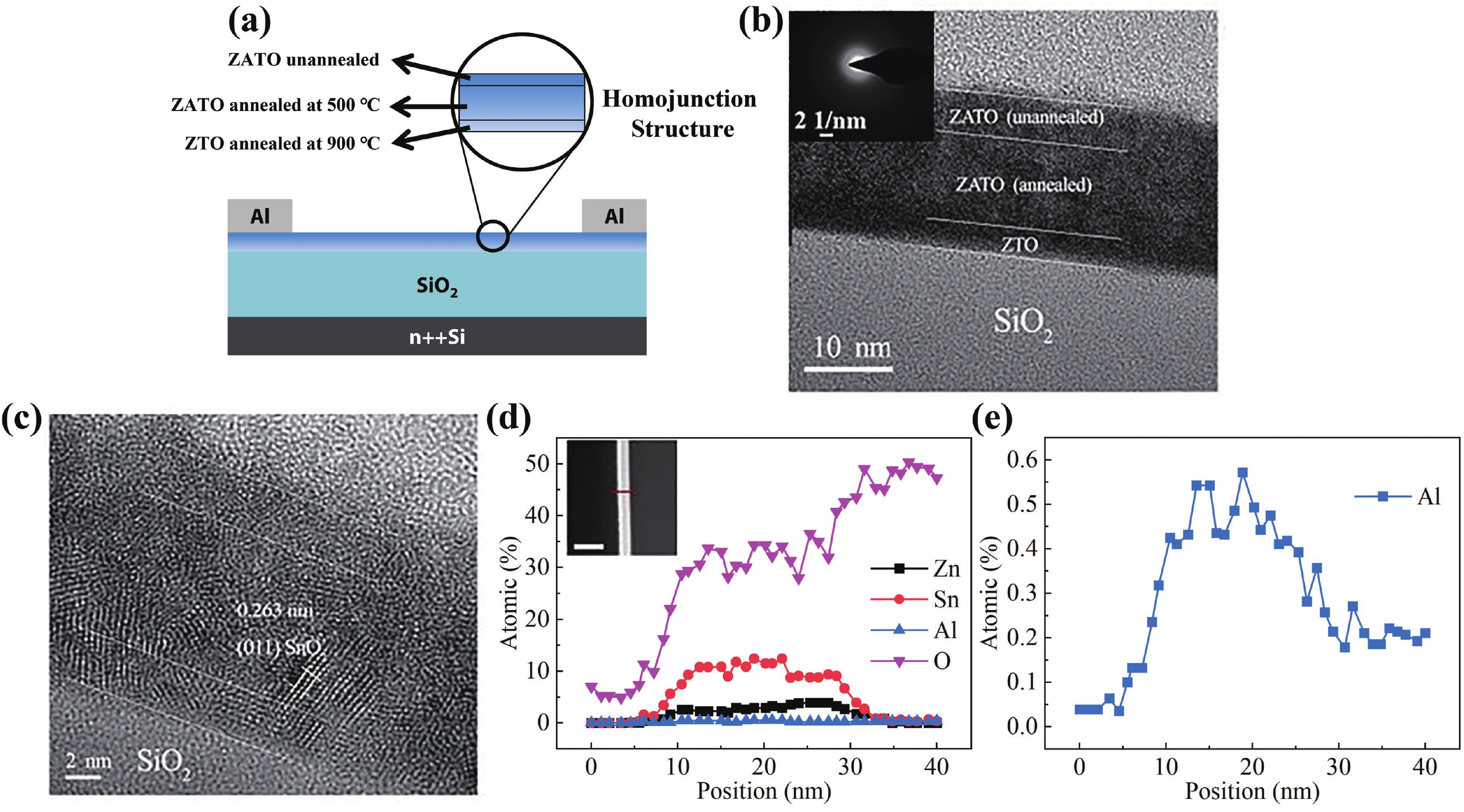
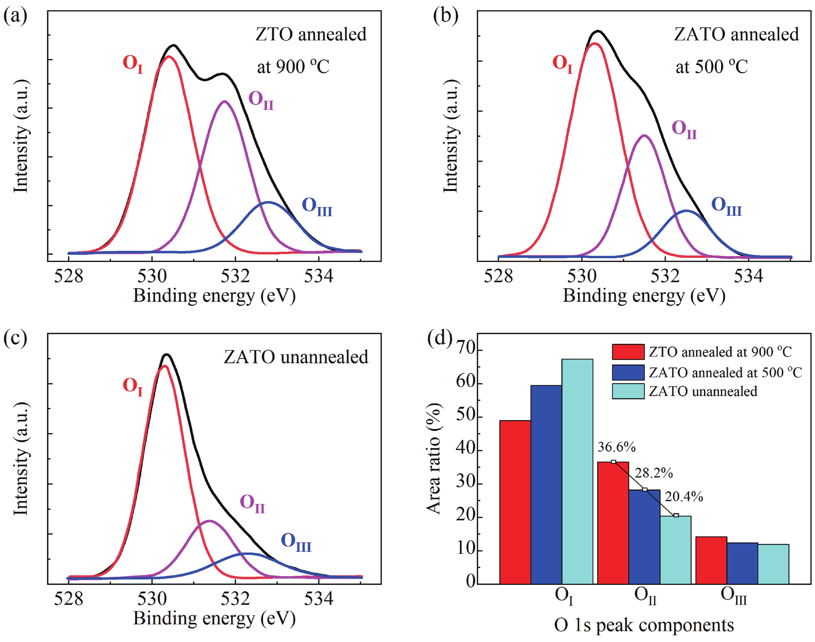
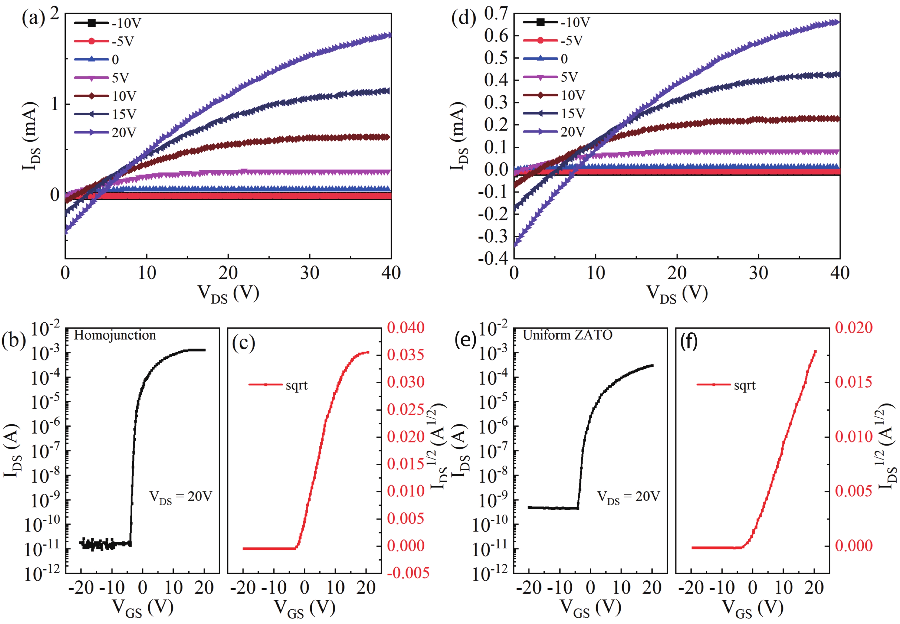
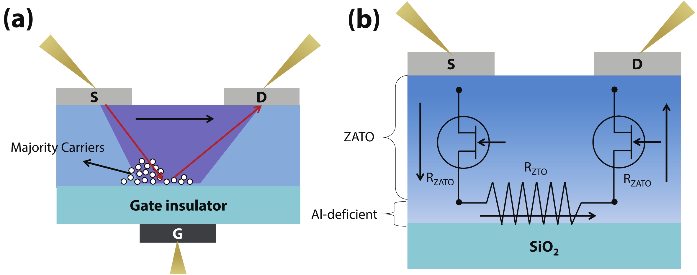
| [1] |
Yue S L, Lu J G, Lu R K, et al. Ultrathin amorphous ZnGe xSnO films for high performance ultra-thin-film transistors. Appl Phys Lett, 2018, 113, 013504 doi: 10.1063/1.5031448 |
| [2] |
Jiang Q J, Feng L S, Wu C J, et al. Amorphous ZnAlSnO thin-film transistors by a combustion solution process for future displays. Appl Phys Lett, 2015, 106, 053503 doi: 10.1063/1.4906999 |
| [3] |
Fortunato E, Barquinha P, Martins R. Oxide semiconductor thin-film transistors: A review of recent advances. Adv Mater, 2012, 24, 2945 doi: 10.1002/adma.201103228 |
| [4] |
Cherenack K H, Kattamis A Z, Hekmatshoar B, et al. Amorphous-silicon thin-film transistors fabricated at 300 °C on a free-standing foil substrate of clear plastic. IEEE Electron Device Lett, 2007, 28, 1004 doi: 10.1109/LED.2007.907411 |
| [5] |
Park J S, Maeng W J, Kim H S, et al. Review of recent developments in amorphous oxide semiconductor thin-film transistor devices. Thin Solid Films, 2012, 520, 1679 doi: 10.1016/j.tsf.2011.07.018 |
| [6] |
Nomura K, Ohta H, Takagi A, et al. Room-temperature fabrication of transparent flexible thin-film transistors using amorphous oxide semiconductors. Nature, 2004, 432, 488 doi: 10.1038/nature03090 |
| [7] |
Kamiya T, Nomura K, Hosono H. Origins of high mobility and low operation voltage of amorphous oxide TFTs: Electronic structure, electron transport, defects and doping. J Disp Technol, 2009, 5, 273 doi: 10.1109/JDT.2009.2021582 |
| [8] |
Kim J I, Ji K H, Jung H Y, et al. Improvement in both mobility and bias stability of ZnSnO transistors by inserting ultra-thin InSnO layer at the gate insulator/channel interface. Appl Phys Lett, 2011, 99, 122102 doi: 10.1063/1.3643054 |
| [9] |
Park S Y, Song J H, Lee C K, et al. Improvement in photo-bias stability of high-mobility indium zinc oxide thin-film transistors by oxygen high-pressure annealing. IEEE Electron Device Lett, 2013, 34, 894 doi: 10.1109/LED.2013.2259574 |
| [10] |
Kim H S, Park J S, Jeong H K, et al. Density of states-based design of metal oxide thin-film transistors for high mobility and superior photostability. ACS Appl Mater Interfaces, 2012, 4, 5416 doi: 10.1021/am301342x |
| [11] |
Song W, Kwon S Y, Myung S, et al. High-mobility ambipolar ZnO-graphene hybrid thin film transistors. Sci Rep, 2014, 4, 4064 doi: 10.1038/srep04064 |
| [12] |
Choi J H, Yang J H, Nam S, et al. InZnO/AlSnZnInO bilayer oxide thin-film transistors with high mobility and high uniformity. IEEE Electron Device Lett, 2016, 37, 1295 doi: 10.1109/LED.2016.2602284 |
| [13] |
Yang J H, Choi J H, Cho S H, et al. Highly stable AlInZnSnO and InZnO double-layer oxide thin-film transistors with mobility over 50 cm 2/(V·s) for high-speed operation. IEEE Electron Device Lett, 2018, 39, 508 doi: 10.1109/LED.2018.2805705 |
| [14] |
Tari A, Wong W S. Effect of dual-dielectric hydrogen-diffusion barrier layers on the performance of low-temperature processed transparent InGaZnO thin-film transistors. Appl Phys Lett, 2018, 112, 073506 doi: 10.1063/1.5000362 |
| [15] |
Zheng Z W, Chen Y C. Improved performances in low-voltage-driven InGaZnO thin film transistors using a SiO 2 buffer layer insertion. Appl Phys A, 2014, 115, 937 doi: 10.1007/s00339-013-7900-3 |
| [16] |
Chiang H Q, Wager J F, Hoffman R L, et al. High mobility transparent thin-film transistors with amorphous zinc tin oxide channel layer. Appl Phys Lett, 2004, 86, 013503 doi: 10.1063/1.1843286 |
| [17] |
Feng L S, Yu G Y, Li X F, et al. Solution processed amorphous ZnSnO thin-film phototransistors. IEEE Trans Electron Devices, 2017, 64, 206 doi: 10.1109/TED.2016.2632742 |
| [18] |
Lu R K, Lu J G, Wei X S, et al. Two-step plasma treatment designed for high-performance flexible amorphous ZnAlSnO thin-film transistors replacing thermal annealing. Adv Electron Mater, 2020, 6, 2000233 doi: 10.1002/aelm.202000233 |
| [19] |
Hong D, Yerubandi G, Chiang H Q, et al. Electrical modeling of thin-film transistors. Crit Rev Solid State Mater Sci, 2008, 33, 101 doi: 10.1080/10408430701384808 |
| [20] |
Kim G H, Shin H S, Du Ahn B, et al. Formation mechanism of solution-processed nanocrystalline InGaZnO thin film as active channel layer in thin-film transistor. J Electrochem Soc, 2009, 156, H7 doi: 10.1149/1.2976027 |
| [21] |
Yeom H I, Ko J B, Mun G, et al. High mobility polycrystalline indium oxide thin-film transistors by means of plasma-enhanced atomic layer deposition. J Mater Chem C, 2016, 4, 6873 doi: 10.1039/C6TC00580B |
| [22] |
Buchholz D B, Ma Q, Alducin D, et al. The structure and properties of amorphous indium oxide. Chem Mater, 2014, 26, 5401 doi: 10.1021/cm502689x |
| [23] |
Kim Y S, Park C H. Rich variety of defects in ZnO via an attractive interaction between O vacancies and Zn interstitials: Origin of n-type doping. Phys Rev Lett, 2009, 102, 086403 doi: 10.1103/PhysRevLett.102.086403 |
| [24] |
Cho D H, Yang S, Byun C, et al. Transparent Al–Zn–Sn–O thin film transistors prepared at low temperature. Appl Phys Lett, 2008, 93, 142111 doi: 10.1063/1.2998612 |
| [25] |
Rim Y S, Kim D L, Jeong W H, et al. Effect of Zr addition on ZnSnO thin-film transistors using a solution process. Appl Phys Lett, 2010, 97, 233502 doi: 10.1063/1.3524514 |
| [26] |
Zhang X J, Zhao H, Song Z X, et al. Insight into the effect of oxygen species and Mn chemical valence over MnO x on the catalytic oxidation of toluene. Appl Surf Sci, 2019, 493, 9 doi: 10.1016/j.apsusc.2019.06.255 |
| [27] |
Wang L B, Cheng B, Zhang L Y, et al. In situ irradiated XPS investigation on S-scheme TiO 2@ZnIn 2S 4 photocatalyst for efficient photocatalytic CO 2 reduction. Small, 2021, 17, 2103447 doi: 10.1002/smll.202103447 |
| [28] |
Jiang Q J, Lu J G, Cheng J P, et al. Combustion-process derived comparable performances of Zn-(In:Sn)-O thin-film transistors with a complete miscibility. Appl Phys Lett, 2014, 105, 132105 doi: 10.1063/1.4896990 |
| [29] |
Chong E, Jo K C, Lee S Y. High stability of amorphous hafnium-indium-zinc-oxide thin film transistor. Appl Phys Lett, 2010, 96, 152102 doi: 10.1063/1.3387819 |
| [30] |
Sheng J Z, Lee H J, Oh S, et al. Flexible and high-performance amorphous indium zinc oxide thin-film transistor using low-temperature atomic layer deposition. ACS Appl Mater Interfaces, 2016, 8, 33821 doi: 10.1021/acsami.6b11774 |
| [31] |
Nayak P K, Hedhili M N, Cha D, et al. High performance solution-deposited amorphous indium gallium zinc oxide thin film transistors by oxygen plasma treatment. Appl Phys Lett, 2012, 100, 202106 doi: 10.1063/1.4718022 |
| [32] |
Yan W C, Yue S L, Lu J G, et al. Thin-film transistors based on amorphous ZnNbSnO films with enhanced behaviors. IEEE Trans Electron Devices, 2016, 63, 2412 doi: 10.1109/TED.2016.2555848 |
| [33] |
Park H W, Chung K B, Park J S. A role of oxygen vacancy on annealed ZnO film in the hydrogen atmosphere. Curr Appl Phys, 2012, 12, S164 doi: 10.1016/j.cap.2012.02.052 |
| [34] |
Park J S, Kim K, Park Y G, et al. Novel ZrInZnO thin-film transistor with excellent stability. Adv Mater, 2009, 21, 329 doi: 10.1002/adma.200802246 |
| [35] |
Park S M, Lee D H, Lim Y S, et al. Effect of aluminum addition to solution-derived amorphous indium zinc oxide thin film for an oxide thin film transistors. Microelectron Eng, 2013, 109, 189 doi: 10.1016/j.mee.2013.03.121 |
| [36] |
Song A, Hong H M, Son K S, et al. Hydrogen behavior in top gate amorphous In–Ga–Zn–O device fabrication process during gate insulator deposition and gate insulator etching. IEEE Trans Electron Devices, 2021, 68, 2723 doi: 10.1109/TED.2021.3074120 |
| [37] |
Yang S, Cho D H, Ryu M K, et al. High-performance Al–Sn–Zn–In–O thin-film transistors: Impact of passivation layer on device stability. IEEE Electron Device Lett, 2010, 31, 144 doi: 10.1109/LED.2009.2036944 |
| [38] |
Michalas L K, Papaioannou G J, Kouvatsos D N, et al. The role of grain boundaries on the performance of poly-Si TFTs. ECS Trans, 2006, 3, 87 doi: 10.1149/1.2356339 |
| [39] |
Yang B S, Park S, Oh S, et al. Improvement of the photo-bias stability of the Zn–Sn–O field effect transistors by an ozone treatment. J Mater Chem, 2012, 22, 10994 doi: 10.1039/c2jm30242j |
| [40] |
Zhang J, Lu J G, Jiang Q J, et al. Stability of amorphous InAlZnO thin-film transistors. J Vac Sci Technol B, 2014, 32, 010602 doi: 10.1116/1.4862150 |
| [41] |
Kim H, Maeng S, Lee S, et al. Improved performance and operational stability of solution-processed InGaSnO (IGTO) thin film transistors by the formation of Sn–O complexes. ACS Appl Electron Mater, 2021, 3, 1199 doi: 10.1021/acsaelm.0c01048 |
| [42] |
Kamiya T, Nomura K, Hosono H. Present status of amorphous In-Ga-Zn-O thin-film transistors. Sci Technol Adv Mater, 2010, 11, 044305 doi: 10.1088/1468-6996/11/4/044305 |
| [43] |
Yue S L, Lu J G, Lu R K, et al. Ultra-thin-film transistors based on ultra-thin amorphous ZnSnO films. Appl Phys A, 2018, 124, 848 doi: 10.1007/s00339-018-2280-3 |
| [44] |
|
| [45] |
Wang W H, Zhang T, Seliverstov A, et al. Layer-dependent optoelectronic properties of 2D van der waals SnS grown by pulsed laser deposition. Adv Electron Mater, 2020, 6, 1901020 doi: 10.1002/aelm.201901020 |
| [46] |
Sheng J Z, Hong T, Lee H M, et al. Amorphous IGZO TFT with high mobility of ~70 cm 2/(V s) via vertical dimension control using PEALD. ACS Appl Mater Interfaces, 2019, 11, 40300 doi: 10.1021/acsami.9b14310 |


 DownLoad:


 Rongkai Lu:received his bachelor’s degree and doctor’s degree at State Key Laboratory of Silicon Materials, School of Materials Science and Engineering, Zhejiang University, China. His current research focuses on amorphous oxide semiconductor, flexible thin film transistor and exploring the possibilities of applications for high-performance TFTs in multiple fields
 Siqin Li:received his Master’s degree at State Key Laboratory of Silicon Materials, School of Materials Science and Engineering, Zhejiang University, China. His current research focuses on amorphous oxide semiconductor, memristor, thin film transistor and their applications for artificial synapses
 Jianguo Lu:has been an associate professor at State Key Laboratory of Silicon Materials, School of Materials Science and Engineering, Zhejiang University, China. His current research focuses on Semiconductor films and transparent electronics, Nanoscale materials and new energies, Coating & biomimetic materials for marine applications. He is Distinguished Young Scholars of Zhejiang Province, China. He is the Member of IEEE. He is the Editorial Board Member of Chinese Chemical Letters and Tungsten. He was awarded 1 Second Prize of National Natural Science Award of China and 3 First Prizes of Science and Technology Award of Zhejiang Province. He was authorized over 50 national invention patents. He published 2 books in Chinese and 1 book chapter in English. He published over 200 SCI papers with citation times over 9000 and H-index of 48. He is the Highly Cited Chinese Researcher
 Yi Zhao:received a bachelor’s degree from Nanjing University of Astronautics and Aeronautics, Nanjing, China, in 2000, a master's degree from Zhejiang University, Hangzhou, China, in 2003, and a Ph.D. from the University of Tokyo, Tokyo, Japan, in 2007, all in materials science and engineering. He currently works with Zhejiang University as a full professor. His recent research interests have mainly focused upon advanced-CMOS devices using new channel materials (strained Si/Ge, SiGe, Ge, and III-V materials) and new structures (SOI, FinFET, UTB, and nanowire)
 Zhizhen Ye:has been an Academician of Chinese Academy of Sciences; Professor at State Key Laboratory of Silicon Materials, School of Materials Science and Engineering, Zhejiang University, China. His current research focuses on Compound semiconductor and optoelectronic materials, Transparent conductive materials, and Semiconductor sensing materials. He is Distinguished Young Scholars of Zhejiang Province, China. He was awarded 1 Second Prize of National Natural Science Award of China, 3 First Prizes of Science and Technology Award of Zhejiang Province, and 2 First Prizes of Science and Technology Award of Ministry of Education of China. He was authorized more than 100 national invention patents. He published 2 books in Chinese and 1 book in English. He published more than 500 papers, cited by over 13000 times with H-index of 63


