


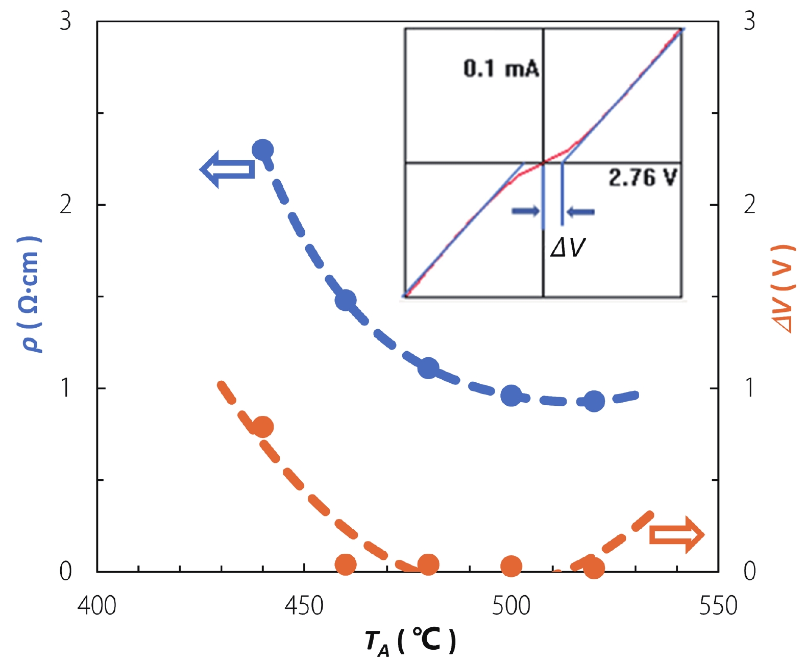
Fig. 1.
(Color online) The effect of different TA on the ρ and ΔV of Hall samples.
ARTICLES
Siyi Huang1, 2, 3, Masao Ikeda2, 3, , Minglong Zhang1, 2, 3, Jianjun Zhu2, 3 and Jianping Liu1, 2, 3,
Corresponding author: Masao Ikeda, mikeda2013@sinano.ac.cn; Jianping Liu, jpliu2010@sinano.ac.cn
Abstract: A suitable contacting scheme for p-(Al)GaN facilitating quick feedback and accurate measurements is proposed in this study. 22 nm p+-GaN followed by 2 nm p-In0.2Ga0.8N was grown on p-type layers by metal-organic chemical vapor deposition. Samples were then cut into squares after annealing and contact electrodes using In balls were put at the corners of the squares. Good linearity between all the electrodes was confirmed in I–V curves during Hall measurements even with In metal. Serval samples taken from the same wafer showed small standard deviation of ~ 4% for resistivity, Hall mobility and hole concentration. The influence of contact layer on the electrical characteristics of bulk p-type layers was then investigated by step etching technique using inductively coupled plasma etching and subsequent Hall-effect measurements. Identical values could be obtained consistently when a 28 nm non-conductive layer thickness at the surface was taken into account. Therefore, the procedures for evaluating the electrical properties of GaN-based p-type layers just using In balls proposed in this study are shown to be quick and useful as for the other conventional III–V materials.
Keywords: GaN, electrical properties, ohmic contact
| [1] |
Amano H, Kito M, Hiramatsu K, et al. P-type conduction in Mg-doped GaN treated with low-energy electron beam irradiation (LEEBI). Jpn J Appl Phys, 1989, 28, L2112 doi: 10.1143/JJAP.28.L2112
|
| [2] |
Nakamura S, Mukai T, Senoh M, et al. Thermal annealing effects on P-type Mg-doped GaN films. Jpn J Appl Phys, 1992, 31, L139 doi: 10.1143/JJAP.31.L139
|
| [3] |
Kumakura K, Kobayashi N. Increased electrical activity of Mg-acceptors in AlxGa1–xN/GaN superlattices. Jpn J Appl Phys, 1999, 38, L1012 doi: 10.1143/JJAP.38.L1012
|
| [4] |
Kumakura K, Makimoto T, Kobayashi N. Activation energy and electrical activity of Mg in Mg-doped InxGa1–xN (x < 0.2). Jpn J Appl Phys, 2000, 39, L337 doi: 10.1143/JJAP.39.L337
|
| [5] |
Nakarmi M L, Kim K H, Li J, et al. Enhanced p-type conduction in GaN and AlGaN by Mg-δ-doping. Appl Phys Lett, 2003, 82, 3041 doi: 10.1063/1.1559444
|
| [6] |
Iida D, Tamura K, Iwaya M, et al. Compensation effect of Mg-doped a- and c-plane GaN films grown by metalorganic vapor phase epitaxy. J Cryst Growth, 2010, 312, 3131 doi: 10.1016/j.jcrysgro.2010.07.038
|
| [7] |
Kinoshita T, Obata T, Yanagi H, et al. High p-type conduction in high-Al content Mg-doped AlGaN. Appl Phys Lett, 2013, 102, 012105 doi: 10.1063/1.4773594
|
| [8] |
Tian A Q, Liu J P, Ikeda M, et al. Conductivity enhancement in AlGaN: Mg by suppressing the incorporation of carbon impurity. Appl Phys Express, 2015, 8, 051001 doi: 10.7567/APEX.8.051001
|
| [9] |
Yang J, Zhao D G, Jiang D S, et al. Different variation behaviors of resistivity for high-temperature-grown and low-temperature-grown p-GaN films. Chin Phys B, 2016, 25, 027102 doi: 10.1088/1674-1056/25/2/027102
|
| [10] |
Narita T, Tomita K, Tokuda Y, et al. The origin of carbon-related carrier compensation in p-type GaN layers grown by MOVPE. J Appl Phys, 2018, 124, 215701 doi: 10.1063/1.5057373
|
| [11] |
Kim J K, Lee J L, Lee J W, et al. Low resistance Pd/Au ohmic contacts to p-type GaN using surface treatment. Appl Phys Lett, 1998, 73, 2953 doi: 10.1063/1.122641
|
| [12] |
Kumakura K, Makimoto T, Kobayashi N. Ohmic contact top-GaN using a strained InGaN contact layer and its thermal stability. Jpn J Appl Phys, 2003, 42, 2254 doi: 10.1143/JJAP.42.2254
|
| [13] |
Li Z C, Huang R, Chen X, et al. The significant effect of carbon and oxygen contaminants at Pd/p-GaN interface on its ohmic contact characteristics. Phys Status Solidi A, 2021, 218, 2000603 doi: 10.1002/pssa.202000603
|
| [14] |
Ho J K, Jong C S, Chiu C C, et al. Low-resistance ohmic contacts to p-type GaN achieved by the oxidation of Ni/Au films. J Appl Phys, 1999, 86, 4491 doi: 10.1063/1.371392
|
| [15] |
Chen L C, Chen F R, Kai J J, et al. Microstructural investigation of oxidized Ni/Au ohmic contact to p-type GaN. J Appl Phys, 1999, 86, 3826 doi: 10.1063/1.371294
|
| [16] |
Ikeda M, Uchida S. Blue-violet laser diodes suitable for blu-ray disk. Phys Stat Sol (a), 2002, 194, 407 doi: 10.1002/1521-396X(200212)194:2<407::AID-PSSA407>3.0.CO;2-N
|
| [17] |
Kumabe T, Ando Y, Watanabe H, et al. Etching-induced damage in heavily Mg-doped p-type GaN and its suppression by low-bias-power inductively coupled plasma-reactive ion etching. Jpn J Appl Phys, 2021, 60, SBBD03 doi: 10.35848/1347-4065/abd538
|
| [18] |
Kent D G, Lee K P, Zhang A P, et al. Effect of N2 plasma treatments on dry etch damage in n- and p-type GaN. Solid State Electron, 2001, 45, 467 doi: 10.1016/S0038-1101(01)00016-8
|
| [19] |
Walukiewicz W, Li S X, Wu J, et al. Optical properties and electronic structure of InN and In-rich group III-nitride alloys. J Cryst Growth, 2004, 269, 119 doi: 10.1016/j.jcrysgro.2004.05.041
|
| [20] |
Bernardini F, Fiorentini V. Spontaneous versus piezoelectric polarization in III-V nitrides: Conceptual aspects and practical consequences. Phys Stat Sol (b), 1999, 216, 391 doi: 10.1002/(SICI)1521-3951(199911)216:1<391::AID-PSSB391>3.0.CO;2-K
|
| [21] |
Fiorentini V, Bernardini F, Ambacher O. Evidence for nonlinear macroscopic polarization in III-V nitride alloy heterostructures. Appl Phys Lett, 2002, 80, 1204 doi: 10.1063/1.1448668
|
| [22] |
Zhang F, Ikeda M, Zhou K, et al. Injection current dependences of electroluminescence transition energy in InGaN/GaN multiple quantum wells light emitting diodes under pulsed current conditions. J Appl Phys, 2015, 118, 033101 doi: 10.1063/1.4926865
|
| [23] |
Zhang M L, Ikeda M, Huang S Y, et al. Ni/Pd-based ohmic contacts to p-GaN through p-InGaN/p+-GaN contacting layers. J Semicond, 2022, 43, 092803 doi: 10.1088/1674-4926/43/9/092803
|
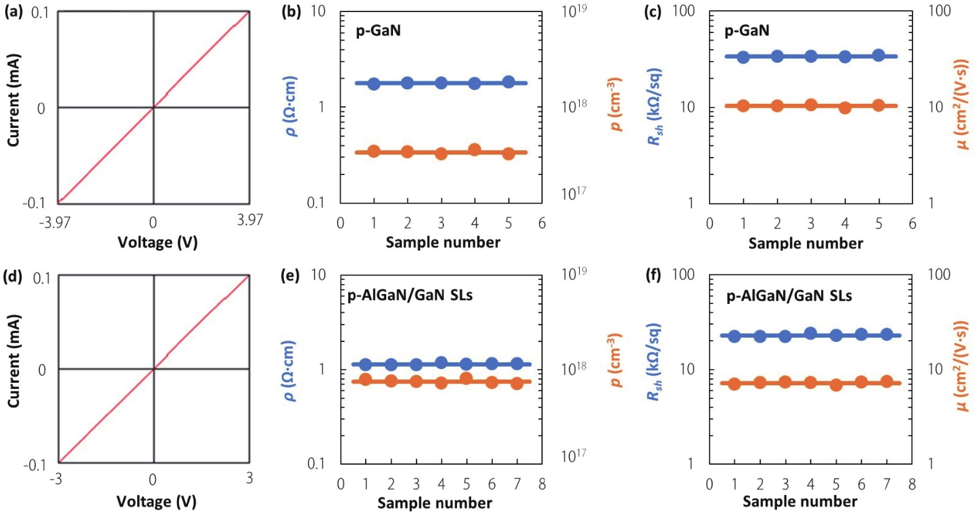
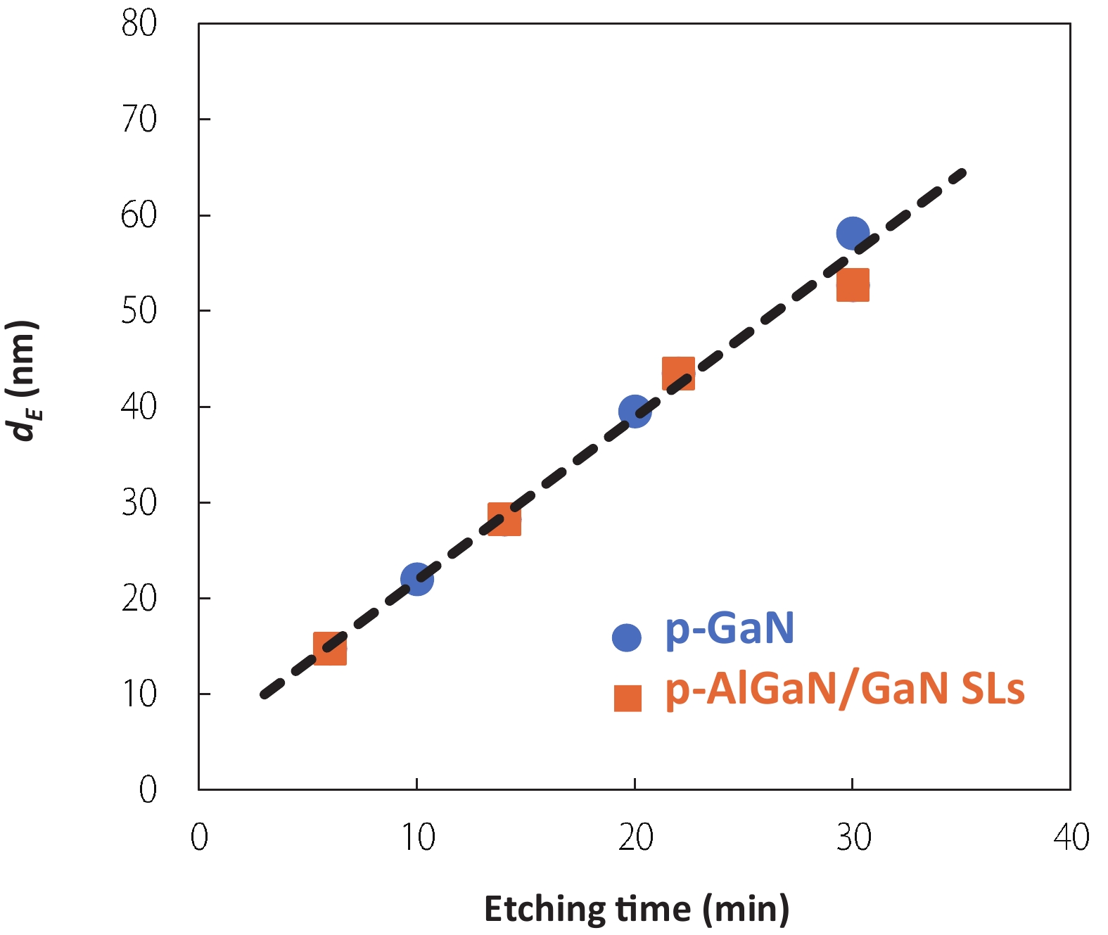

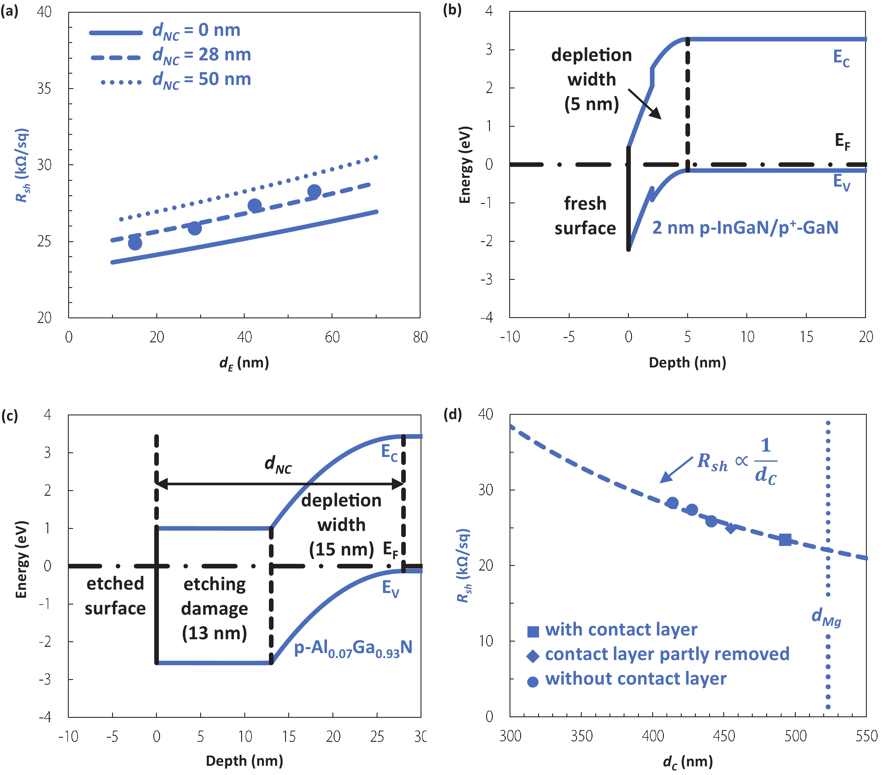
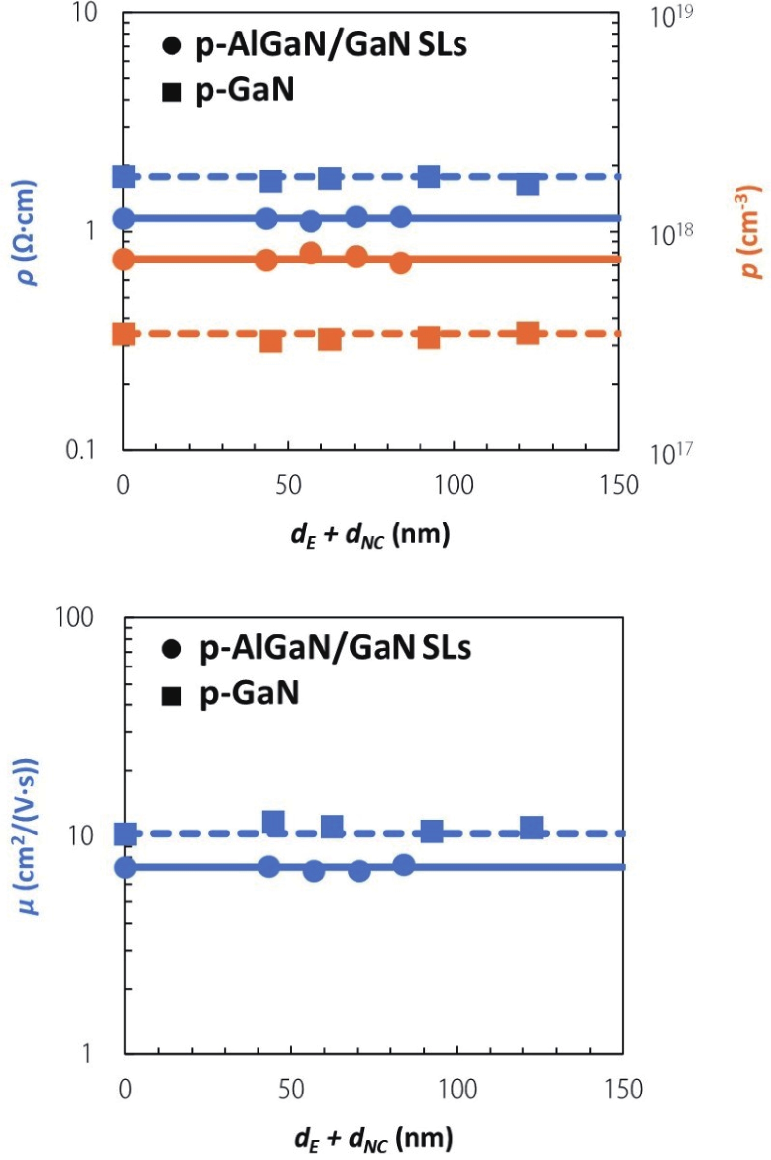
Table 1. The detailed electrical properties of AlGaN/GaN SLs samples.
| Parameter | ρ (Ω·cm) | μ (cm2/(V·s)) | p (cm−3) | Rsh (kΩ/sq) | dC (nm) | Etching |
| A1 – A4 (average) | 1.16 | 7.23 | 7.49×10¹⁷ | 23.4 | 493 | No |
| A1 | 1.16 | 7.31 | 7.39×10¹⁷ | 24.9 | 455 | Yes |
| A2 | 1.12 | 6.95 | 8.03×10¹⁷ | 25.9 | 441 | Yes |
| A3 | 1.17 | 6.95 | 7.66×10¹⁷ | 27.4 | 428 | Yes |
| A4 | 1.18 | 7.40 | 7.18×10¹⁷ | 28.3 | 414 | Yes |
 DownLoad: CSV
| [1] |
Amano H, Kito M, Hiramatsu K, et al. P-type conduction in Mg-doped GaN treated with low-energy electron beam irradiation (LEEBI). Jpn J Appl Phys, 1989, 28, L2112 doi: 10.1143/JJAP.28.L2112
|
| [2] |
Nakamura S, Mukai T, Senoh M, et al. Thermal annealing effects on P-type Mg-doped GaN films. Jpn J Appl Phys, 1992, 31, L139 doi: 10.1143/JJAP.31.L139
|
| [3] |
Kumakura K, Kobayashi N. Increased electrical activity of Mg-acceptors in AlxGa1–xN/GaN superlattices. Jpn J Appl Phys, 1999, 38, L1012 doi: 10.1143/JJAP.38.L1012
|
| [4] |
Kumakura K, Makimoto T, Kobayashi N. Activation energy and electrical activity of Mg in Mg-doped InxGa1–xN (x < 0.2). Jpn J Appl Phys, 2000, 39, L337 doi: 10.1143/JJAP.39.L337
|
| [5] |
Nakarmi M L, Kim K H, Li J, et al. Enhanced p-type conduction in GaN and AlGaN by Mg-δ-doping. Appl Phys Lett, 2003, 82, 3041 doi: 10.1063/1.1559444
|
| [6] |
Iida D, Tamura K, Iwaya M, et al. Compensation effect of Mg-doped a- and c-plane GaN films grown by metalorganic vapor phase epitaxy. J Cryst Growth, 2010, 312, 3131 doi: 10.1016/j.jcrysgro.2010.07.038
|
| [7] |
Kinoshita T, Obata T, Yanagi H, et al. High p-type conduction in high-Al content Mg-doped AlGaN. Appl Phys Lett, 2013, 102, 012105 doi: 10.1063/1.4773594
|
| [8] |
Tian A Q, Liu J P, Ikeda M, et al. Conductivity enhancement in AlGaN: Mg by suppressing the incorporation of carbon impurity. Appl Phys Express, 2015, 8, 051001 doi: 10.7567/APEX.8.051001
|
| [9] |
Yang J, Zhao D G, Jiang D S, et al. Different variation behaviors of resistivity for high-temperature-grown and low-temperature-grown p-GaN films. Chin Phys B, 2016, 25, 027102 doi: 10.1088/1674-1056/25/2/027102
|
| [10] |
Narita T, Tomita K, Tokuda Y, et al. The origin of carbon-related carrier compensation in p-type GaN layers grown by MOVPE. J Appl Phys, 2018, 124, 215701 doi: 10.1063/1.5057373
|
| [11] |
Kim J K, Lee J L, Lee J W, et al. Low resistance Pd/Au ohmic contacts to p-type GaN using surface treatment. Appl Phys Lett, 1998, 73, 2953 doi: 10.1063/1.122641
|
| [12] |
Kumakura K, Makimoto T, Kobayashi N. Ohmic contact top-GaN using a strained InGaN contact layer and its thermal stability. Jpn J Appl Phys, 2003, 42, 2254 doi: 10.1143/JJAP.42.2254
|
| [13] |
Li Z C, Huang R, Chen X, et al. The significant effect of carbon and oxygen contaminants at Pd/p-GaN interface on its ohmic contact characteristics. Phys Status Solidi A, 2021, 218, 2000603 doi: 10.1002/pssa.202000603
|
| [14] |
Ho J K, Jong C S, Chiu C C, et al. Low-resistance ohmic contacts to p-type GaN achieved by the oxidation of Ni/Au films. J Appl Phys, 1999, 86, 4491 doi: 10.1063/1.371392
|
| [15] |
Chen L C, Chen F R, Kai J J, et al. Microstructural investigation of oxidized Ni/Au ohmic contact to p-type GaN. J Appl Phys, 1999, 86, 3826 doi: 10.1063/1.371294
|
| [16] |
Ikeda M, Uchida S. Blue-violet laser diodes suitable for blu-ray disk. Phys Stat Sol (a), 2002, 194, 407 doi: 10.1002/1521-396X(200212)194:2<407::AID-PSSA407>3.0.CO;2-N
|
| [17] |
Kumabe T, Ando Y, Watanabe H, et al. Etching-induced damage in heavily Mg-doped p-type GaN and its suppression by low-bias-power inductively coupled plasma-reactive ion etching. Jpn J Appl Phys, 2021, 60, SBBD03 doi: 10.35848/1347-4065/abd538
|
| [18] |
Kent D G, Lee K P, Zhang A P, et al. Effect of N2 plasma treatments on dry etch damage in n- and p-type GaN. Solid State Electron, 2001, 45, 467 doi: 10.1016/S0038-1101(01)00016-8
|
| [19] |
Walukiewicz W, Li S X, Wu J, et al. Optical properties and electronic structure of InN and In-rich group III-nitride alloys. J Cryst Growth, 2004, 269, 119 doi: 10.1016/j.jcrysgro.2004.05.041
|
| [20] |
Bernardini F, Fiorentini V. Spontaneous versus piezoelectric polarization in III-V nitrides: Conceptual aspects and practical consequences. Phys Stat Sol (b), 1999, 216, 391 doi: 10.1002/(SICI)1521-3951(199911)216:1<391::AID-PSSB391>3.0.CO;2-K
|
| [21] |
Fiorentini V, Bernardini F, Ambacher O. Evidence for nonlinear macroscopic polarization in III-V nitride alloy heterostructures. Appl Phys Lett, 2002, 80, 1204 doi: 10.1063/1.1448668
|
| [22] |
Zhang F, Ikeda M, Zhou K, et al. Injection current dependences of electroluminescence transition energy in InGaN/GaN multiple quantum wells light emitting diodes under pulsed current conditions. J Appl Phys, 2015, 118, 033101 doi: 10.1063/1.4926865
|
| [23] |
Zhang M L, Ikeda M, Huang S Y, et al. Ni/Pd-based ohmic contacts to p-GaN through p-InGaN/p+-GaN contacting layers. J Semicond, 2022, 43, 092803 doi: 10.1088/1674-4926/43/9/092803
|


Article views: 1387 Times PDF downloads: 91 Times Cited by: 0 Times
Received: 28 October 2022 Revised: 29 January 2023 Online: Accepted Manuscript: 15 February 2023Uncorrected proof: 16 February 2023Published: 10 May 2023
| Citation: |
Siyi Huang, Masao Ikeda, Minglong Zhang, Jianjun Zhu, Jianping Liu. Suitable contacting scheme for evaluating electrical properties of GaN-based p-type layers[J]. Journal of Semiconductors, 2023, 44(5): 052802. doi: 10.1088/1674-4926/44/5/052802
****
S Y Huang, M Ikeda, M L Zhang, J J Zhu, J P Liu. Suitable contacting scheme for evaluating electrical properties of GaN-based p-type layers[J]. J. Semicond, 2023, 44(5): 052802. doi: 10.1088/1674-4926/44/5/052802

|
 Siyi Huang:got his bachelor's degree in 2011 from University of Science and Technology Beijing and his master’s degree in 2014 from City University of Hong Kong. Now he is a doctoral student at University of Science and Technology of China under the supervision of Prof. Masao Ikeda and Prof. Jianping Liu. His research focuses on MOCVD growth and characterization of GaN-based materials
 Masao Ikeda:received his doctoral degree from Waseda University, Tokyo, Japan, in 1991. He is currently a Professor with the Suzhou Institute of Nano-Tech and Nano-Bionics, Chinese Academy of Sciences, Suzhou, China. His current research interests include III–V compound semiconductor materials and devices
 Jianping Liu:is a professor in Suzhou Institute of Nano-Tech and Nano-Bionics, Chinese Academy of Sciences. He earned his doctoral degree from Institute of Semiconductors, Chinese Academy of Sciences in 2004. He worked at Lab of Optoelectronics Technology at Beijing University of Technology from 2004 to 2006. He did postdoctoral research in Department of Electrical Engineering at Georgia Institute of Technology from 2006 to 2010. His research interests include MOCVD growth, GaN-based materials and devices
| [1] |
Amano H, Kito M, Hiramatsu K, et al. P-type conduction in Mg-doped GaN treated with low-energy electron beam irradiation (LEEBI). Jpn J Appl Phys, 1989, 28, L2112 doi: 10.1143/JJAP.28.L2112
|
| [2] |
Nakamura S, Mukai T, Senoh M, et al. Thermal annealing effects on P-type Mg-doped GaN films. Jpn J Appl Phys, 1992, 31, L139 doi: 10.1143/JJAP.31.L139
|
| [3] |
Kumakura K, Kobayashi N. Increased electrical activity of Mg-acceptors in AlxGa1–xN/GaN superlattices. Jpn J Appl Phys, 1999, 38, L1012 doi: 10.1143/JJAP.38.L1012
|
| [4] |
Kumakura K, Makimoto T, Kobayashi N. Activation energy and electrical activity of Mg in Mg-doped InxGa1–xN (x < 0.2). Jpn J Appl Phys, 2000, 39, L337 doi: 10.1143/JJAP.39.L337
|
| [5] |
Nakarmi M L, Kim K H, Li J, et al. Enhanced p-type conduction in GaN and AlGaN by Mg-δ-doping. Appl Phys Lett, 2003, 82, 3041 doi: 10.1063/1.1559444
|
| [6] |
Iida D, Tamura K, Iwaya M, et al. Compensation effect of Mg-doped a- and c-plane GaN films grown by metalorganic vapor phase epitaxy. J Cryst Growth, 2010, 312, 3131 doi: 10.1016/j.jcrysgro.2010.07.038
|
| [7] |
Kinoshita T, Obata T, Yanagi H, et al. High p-type conduction in high-Al content Mg-doped AlGaN. Appl Phys Lett, 2013, 102, 012105 doi: 10.1063/1.4773594
|
| [8] |
Tian A Q, Liu J P, Ikeda M, et al. Conductivity enhancement in AlGaN: Mg by suppressing the incorporation of carbon impurity. Appl Phys Express, 2015, 8, 051001 doi: 10.7567/APEX.8.051001
|
| [9] |
Yang J, Zhao D G, Jiang D S, et al. Different variation behaviors of resistivity for high-temperature-grown and low-temperature-grown p-GaN films. Chin Phys B, 2016, 25, 027102 doi: 10.1088/1674-1056/25/2/027102
|
| [10] |
Narita T, Tomita K, Tokuda Y, et al. The origin of carbon-related carrier compensation in p-type GaN layers grown by MOVPE. J Appl Phys, 2018, 124, 215701 doi: 10.1063/1.5057373
|
| [11] |
Kim J K, Lee J L, Lee J W, et al. Low resistance Pd/Au ohmic contacts to p-type GaN using surface treatment. Appl Phys Lett, 1998, 73, 2953 doi: 10.1063/1.122641
|
| [12] |
Kumakura K, Makimoto T, Kobayashi N. Ohmic contact top-GaN using a strained InGaN contact layer and its thermal stability. Jpn J Appl Phys, 2003, 42, 2254 doi: 10.1143/JJAP.42.2254
|
| [13] |
Li Z C, Huang R, Chen X, et al. The significant effect of carbon and oxygen contaminants at Pd/p-GaN interface on its ohmic contact characteristics. Phys Status Solidi A, 2021, 218, 2000603 doi: 10.1002/pssa.202000603
|
| [14] |
Ho J K, Jong C S, Chiu C C, et al. Low-resistance ohmic contacts to p-type GaN achieved by the oxidation of Ni/Au films. J Appl Phys, 1999, 86, 4491 doi: 10.1063/1.371392
|
| [15] |
Chen L C, Chen F R, Kai J J, et al. Microstructural investigation of oxidized Ni/Au ohmic contact to p-type GaN. J Appl Phys, 1999, 86, 3826 doi: 10.1063/1.371294
|
| [16] |
Ikeda M, Uchida S. Blue-violet laser diodes suitable for blu-ray disk. Phys Stat Sol (a), 2002, 194, 407 doi: 10.1002/1521-396X(200212)194:2<407::AID-PSSA407>3.0.CO;2-N
|
| [17] |
Kumabe T, Ando Y, Watanabe H, et al. Etching-induced damage in heavily Mg-doped p-type GaN and its suppression by low-bias-power inductively coupled plasma-reactive ion etching. Jpn J Appl Phys, 2021, 60, SBBD03 doi: 10.35848/1347-4065/abd538
|
| [18] |
Kent D G, Lee K P, Zhang A P, et al. Effect of N2 plasma treatments on dry etch damage in n- and p-type GaN. Solid State Electron, 2001, 45, 467 doi: 10.1016/S0038-1101(01)00016-8
|
| [19] |
Walukiewicz W, Li S X, Wu J, et al. Optical properties and electronic structure of InN and In-rich group III-nitride alloys. J Cryst Growth, 2004, 269, 119 doi: 10.1016/j.jcrysgro.2004.05.041
|
| [20] |
Bernardini F, Fiorentini V. Spontaneous versus piezoelectric polarization in III-V nitrides: Conceptual aspects and practical consequences. Phys Stat Sol (b), 1999, 216, 391 doi: 10.1002/(SICI)1521-3951(199911)216:1<391::AID-PSSB391>3.0.CO;2-K
|
| [21] |
Fiorentini V, Bernardini F, Ambacher O. Evidence for nonlinear macroscopic polarization in III-V nitride alloy heterostructures. Appl Phys Lett, 2002, 80, 1204 doi: 10.1063/1.1448668
|
| [22] |
Zhang F, Ikeda M, Zhou K, et al. Injection current dependences of electroluminescence transition energy in InGaN/GaN multiple quantum wells light emitting diodes under pulsed current conditions. J Appl Phys, 2015, 118, 033101 doi: 10.1063/1.4926865
|
| [23] |
Zhang M L, Ikeda M, Huang S Y, et al. Ni/Pd-based ohmic contacts to p-GaN through p-InGaN/p+-GaN contacting layers. J Semicond, 2022, 43, 092803 doi: 10.1088/1674-4926/43/9/092803
|

 WeChat ID
Journal of Semiconductors © 2017 All Rights Reserved 京ICP备05085259号-2


