J. Semicond. > 2023, Volume 44 > Issue 8 > 080501

SHORT COMMUNICATION

Solution-processed CuIn(S,Se)2 solar cells on transparent electrode offering 9.4% efficiency

Xinge Liu1, §, Chengfeng Ma1, §, Hao Xin1, and Liming Ding2,

+ Author Affiliations

 Corresponding author: Hao Xin, iamhxin@njupt.edu.cn; Liming Ding, ding@nanoctr.cn

DOI: 10.1088/1674-4926/44/8/080501

PDF

Turn off MathJax

Chalcopyrite, copper indium gallium selenide (Cu(In,Ga)Se2, CIGS), as semiconductor materials, have been widely used as absorbers in thin-film solar cells, offering high power conversion efficiency (PCE) and good thermal stability[1-3]. Recently, the development of non-traditional photovoltaic (PV) devices such as semitransparent, bifacial, tandem and flexible solar cells, has expanded the application scenarios of thin-film solar cells. For example, semitransparent chalcopyrite solar cells can be applied to building exteriors such as windows and skylights, which can convert a portion of sunlight into electricity while transmit the remaining into the building. Traditional chalcopyrite thin-film solar cells are fabricated on opaque Mo back contact, either by vacuum[2] or solution[3] methods, which completely blocks sunlight. To allow light transmission, replacing traditional Mo back contact with transparent electrodes, such as indium tin oxide (ITO), aluminum-doped zinc oxide (AZO), and fluorine-doped tin oxide (FTO), is necessary. Moreover, the vacuum methods, such as co-evaporation[4] and sputtering[5], generally require expensive equipment and high-temperature deposition that lead to high energy input, large capital investment, and operational costs. Solution processing such as spin-coating[6], blade-coating[7], spray pyrolysis[8] and inkjet-printing[9] is more suitable for fabricating chalcopyrite solar cells on transparent electrodes because of the simple preparation, low cost and substrate shape friendly. However, the so-far reported solution-processed chalcopyrite solar cells exhibit low efficiency[10-12] on transparent substrate (8.0%)[12]. In this work, we report the fabrication of CuIn(S,Se)2 (CISSe) solar cells on FTO substrate from DMF solution. The CISSe film was directly deposited on commercial FTO substrates by simple spin-coating followed by recrystallization at the atmosphere of selenium gas (selenization)[13]. The solar cells with a structure of FTO/CISSe/CdS/i-ZnO/ITO/Ni/Al offered an 9.40% PCE without anti-reflective coating, which is the highest efficiency for solution-processed CISSe thin-film solar cells on transparent electrodes.

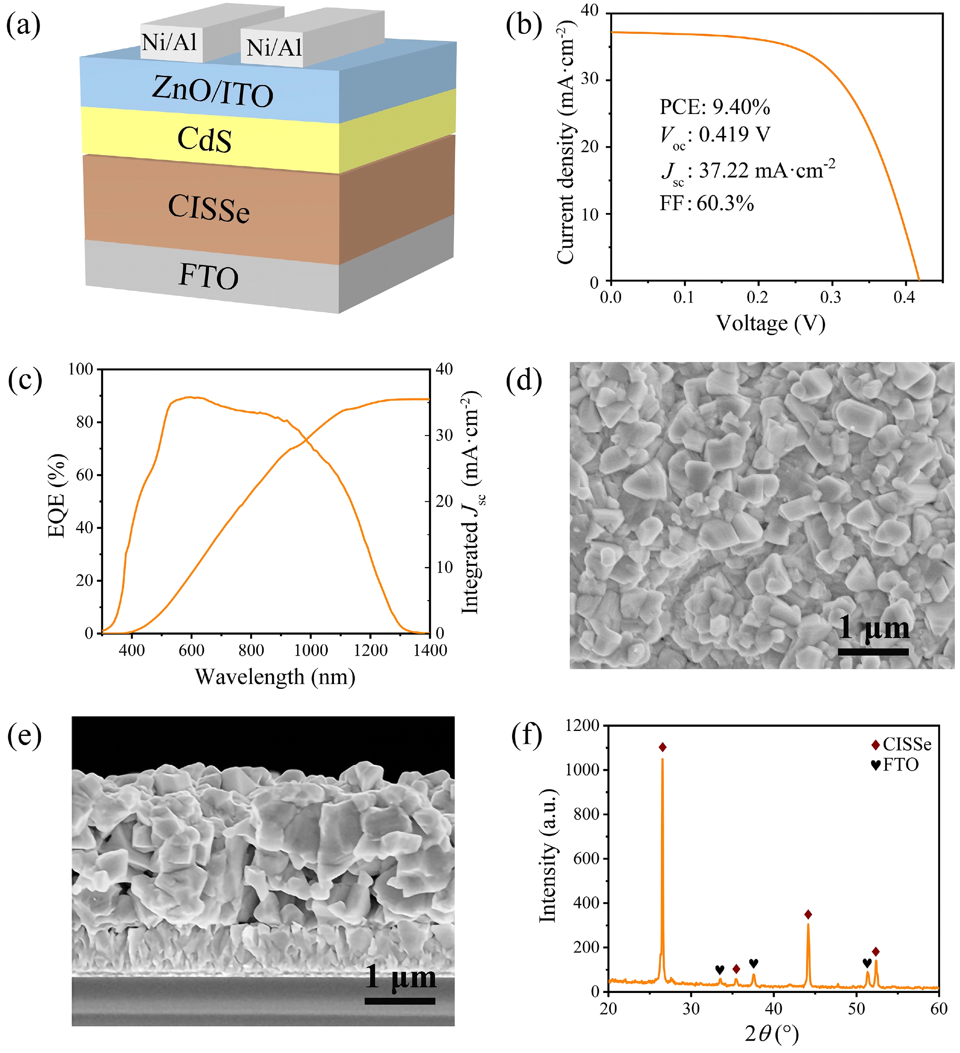
Fig. 1(a) illustrates the device structure of CISSe solar cells on FTO. The device has a structure of FTO/CISSe/CdS/i-ZnO/ITO/Ni/Al. The CISSe film was made on FTO substrate by using DMF precursor solution (details were given in SI). Figs. 1(b) and 1(c) show the current density-voltage (J-V) curve and the external quantum efficiency (EQE) spectrum of the best CISSe solar cell on FTO. An 9.40% PCE with an open circuit voltage (Voc) of 0.419 V, a short-circuit current density (Jsc) of 37.22 mA·cm−2, and a fill factor (FF) of 60.3%, has been achieved without an anti-reflective coating. This is the highest efficiency for solution-processed chalcopyrite solar cells on transparent substrates. The device has a good EQE response over 70% at 500−1000 nm with a peak value close to 90%. The integrated Jsc from EQE spectrum is 35.48 mA·cm−2, in good agreement with the Jsc from J-V characterization. The bandgap of CISSe absorber obtained by extending the linear portion of (ln(1-EQE))2 versus energy plot is 1.03 eV, very close to the Eg for pure CuInSe2 (1.04 eV), demonstrating a sufficient transformation from copper indium sulfide (CIS) to CISe during selenization. The Urbach energy (EU) of the CISSe absorber estimated from the sub-bandgap region by plotting ln(−ln(1-EQE)) versus energy is 20.17 meV, revealing small band tailing (Fig. S1).

Fig. 1.  (Color online) (a) The structure for CISSe solar cells. The J-V curve (b) and the EQE spectrum (c) for the best CISSe solar cell on FTO. Inset: extraction of the bandgap (Eg) from the EQE spectrum. The top-view (d) and cross-sectional (e) SEM images for CISSe film on FTO. (f) The XRD patterns for CISSe film on FTO.

Figs. 1(d) and 1(e) show the top-view and cross-sectional scanning electron microscopy (SEM) images for the CISSe absorber on FTO substrate. From Fig. 1(d), it can be seen that the CISSe is composed of compact grains with a dense and flat surface, which is conducive for deposition of buffer layer and formation of high-quality heterojunction. Fig. 1(e) shows that the film has excellent adherence to FTO substrate. It is worth noting that for kesterite copper zinc tin sulfoselenide Cu2ZnSn(S,Se)4 (CZTSSe) solar cells on FTO substrate, a MoO3 interfacial layer between absorber and FTO is needed to faciliate grain growth and improve device performance[14]. For CISSe solar cells here, a MoO3 interfacial layer significantly reduces device performance (Fig. S2), indicating different grain growth mechanism. The excellent adherence and grain growth of CISSe on bare FTO substrate indicates that an interfacial layer between CISSe and back contact is not necessary, which is an advantage for transparent CISSe solar cells.

Fig. 1(f) shows the XRD patterns for CISSe absorber on FTO substrate. Except for the diffraction peaks of FTO, other diffraction peaks can be assigned to chalcopyrite CuInSe2 phase (JCPDS#40-1487) with a preferred orientation along the (112) plane. The crystalline size of CISSe calculated from the (112) diffraction via Scherrer equation is 65 nm. The large crystalline size confirms the high quality of CISSe film, which is consistent with the SEM results. The high-quality absorber film benefits from the direct phase transformation in grain growth[15], which can greatly reduce grain boundaries and charge recombination. The conductivity of FTO (Table S1) showed small change after selenization, indicating a high tolerance of FTO to the selenization temperature.

Compared with devices on Mo substrate, the efficiency for CISSe solar cells on transparent FTO substrate is relatively low. There is still much room for improving the performance of these FTO-based chalcopyrite devices, e.g., introducing alkali metal ions to facilitate grain growth, and using Ga gradient to enhance Voc[16,17]. These strategies will be conducted in our future work to further improve the device performance.

This work is supported by the National Natural Science Foundation of China (22075150) and the National Key Research and Development Program of China (2019YFE0118100). L. Ding thanks the National Key Research and Development Program of China (2022YFB3803300), the open research fund of Songshan Lake Materials Laboratory (2021SLABFK02), and the National Natural Science Foundation of China (21961160720).

Supplementary materials to this article can be found on-line at https://doi.org/1674-4926/44/8/080501.


[1]
Suresh S, Uhl A R. Present status of solution-processing routes for Cu(In,Ga)(S,Se)2 solar cell absorbers. Adv Energy Mater, 2021, 11(14), 2003743 doi: 10.1002/aenm.202003743
[2]
Nakamura M, Yamaguchi K, Kimoto Y, et al. Cd-free Cu(In,Ga)(Se,S)2 thin-film solar cell with record efficiency of 23.35%. IEEE J Photovolt, 2019, 9(6), 1863 doi: 10.1109/JPHOTOV.2019.2937218
[3]
Ramanujam J, Singh U P. Copper indium gallium selenide based solar cells–a review. Energy Environ Sci, 2017, 10, 1306 doi: 10.1039/C7EE00826K
[4]
Repins I, Contreras M A, Egaas B, et al. 19.9%-efficient ZnO/CdS/CuInGaSe2 solar cell with 81.2% fill factor. Prog Photovolt Res Appl, 2008, 16, 235 doi: 10.1002/pip.822
[5]
Chirilă A, Reinhard P, Pianezzi F, et al. Potassium-induced surface modification of Cu(In,Ga)Se2 thin films for high-efficiency solar cells. Nat Mater, 2013, 12, 1107 doi: 10.1038/nmat3789
[6]
Jiang J J, Giridharagopal R, Jedlicka E, et al. Highly efficient copper-rich chalcopyrite solar cells from DMF molecular solution. Nano Energy, 2020, 69, 104438 doi: 10.1016/j.nanoen.2019.104438
[7]
Ma C F, Xiang C X, Liu X G, et al. Over 12% efficient CuIn(S,Se)2 solar cell with the absorber fabricated from dimethylformamide solution by doctor-blading in ambient air. Sol RRL, 2022, 6(6), 2200150 doi: 10.1002/solr.202200150
[8]
Arnou P, van Hest M F A M, Cooper C S, et al. Hydrazine-free solution-deposited CuIn(S,Se)2 solar cells by spray deposition of metal chalcogenides. ACS Appl Mater Interfaces, 2016, 8(19), 11893 doi: 10.1021/acsami.6b01541
[9]
Lin X Z, Klenk R, Wang L, et al. 11.3% efficiency Cu(In,Ga)(S,Se)2 thin film solar cells via drop-on-demand inkjet printing. Energy Environ Sci, 2016, 9, 2037 doi: 10.1039/C6EE00587J
[10]
Moon S H, Park S J, Hwang Y J, et al. Printable, wide band-gap chalcopyrite thin films for power generating window applications. Sci Rep, 2014, 4, 4408 doi: 10.1038/srep04408
[11]
Ben Chu V, Park S J, Park G S, et al. Semi-transparent thin film solar cells by a solution process. Korean J Chem Eng, 2016, 33(3), 880 doi: 10.1007/s11814-015-0200-1
[12]
Gao Y, Yin G C, Li Y, et al. 8.0% efficient submicron CuIn(S,Se)2 solar cells on Sn: In2O3 back contact via a facile solution process. ACS Appl Energy Mater, 2022, 5(10), 12252 doi: 10.1021/acsaem.2c01764
[13]
Jiang J J, Yu S T, Gong Y C, et al. 10.3% efficient CuIn(S,Se)2 solar cells from DMF molecular solution with the absorber selenized under high argon pressure. Sol RRL, 2018, 2, 1800044 doi: 10.1002/solr.201800044
[14]
Zhou Y G, Xiang C X, Dai Q, et al. 11.4% efficiency kesterite solar cells on transparent electrode. Adv Energy Mater, 2023, 13, 2370079 doi: 10.1002/aenm.202370079
[15]
Yu S T, Li B Y, Jiang J J, et al. Solution-processed chalcopyrite solar cells: The grain growth mechanism and the effects of Cu/In mole ratio. Adv Energy Mater, 2022, 12, 2103644 doi: 10.1002/aenm.202103644
[16]
Wang Y Z, Lv S S, Li Z C. Review on incorporation of alkali elements and their effects in Cu(In,Ga)Se2 solar cells. J Mater Sci Technol, 2022, 96(10), 179 doi: 10.1016/j.jmst.2020.07.050
[17]
Witte W, Abou-Ras D, Albe K, et al. Gallium gradients in Cu(In,Ga)Se2 thin-film solar cells. Prog Photovolt Res Appl, 2015, 23(6), 717 doi: 10.1002/pip.2485
Fig. 1.  (Color online) (a) The structure for CISSe solar cells. The J-V curve (b) and the EQE spectrum (c) for the best CISSe solar cell on FTO. Inset: extraction of the bandgap (Eg) from the EQE spectrum. The top-view (d) and cross-sectional (e) SEM images for CISSe film on FTO. (f) The XRD patterns for CISSe film on FTO.

[1]
Suresh S, Uhl A R. Present status of solution-processing routes for Cu(In,Ga)(S,Se)2 solar cell absorbers. Adv Energy Mater, 2021, 11(14), 2003743 doi: 10.1002/aenm.202003743
[2]
Nakamura M, Yamaguchi K, Kimoto Y, et al. Cd-free Cu(In,Ga)(Se,S)2 thin-film solar cell with record efficiency of 23.35%. IEEE J Photovolt, 2019, 9(6), 1863 doi: 10.1109/JPHOTOV.2019.2937218
[3]
Ramanujam J, Singh U P. Copper indium gallium selenide based solar cells–a review. Energy Environ Sci, 2017, 10, 1306 doi: 10.1039/C7EE00826K
[4]
Repins I, Contreras M A, Egaas B, et al. 19.9%-efficient ZnO/CdS/CuInGaSe2 solar cell with 81.2% fill factor. Prog Photovolt Res Appl, 2008, 16, 235 doi: 10.1002/pip.822
[5]
Chirilă A, Reinhard P, Pianezzi F, et al. Potassium-induced surface modification of Cu(In,Ga)Se2 thin films for high-efficiency solar cells. Nat Mater, 2013, 12, 1107 doi: 10.1038/nmat3789
[6]
Jiang J J, Giridharagopal R, Jedlicka E, et al. Highly efficient copper-rich chalcopyrite solar cells from DMF molecular solution. Nano Energy, 2020, 69, 104438 doi: 10.1016/j.nanoen.2019.104438
[7]
Ma C F, Xiang C X, Liu X G, et al. Over 12% efficient CuIn(S,Se)2 solar cell with the absorber fabricated from dimethylformamide solution by doctor-blading in ambient air. Sol RRL, 2022, 6(6), 2200150 doi: 10.1002/solr.202200150
[8]
Arnou P, van Hest M F A M, Cooper C S, et al. Hydrazine-free solution-deposited CuIn(S,Se)2 solar cells by spray deposition of metal chalcogenides. ACS Appl Mater Interfaces, 2016, 8(19), 11893 doi: 10.1021/acsami.6b01541
[9]
Lin X Z, Klenk R, Wang L, et al. 11.3% efficiency Cu(In,Ga)(S,Se)2 thin film solar cells via drop-on-demand inkjet printing. Energy Environ Sci, 2016, 9, 2037 doi: 10.1039/C6EE00587J
[10]
Moon S H, Park S J, Hwang Y J, et al. Printable, wide band-gap chalcopyrite thin films for power generating window applications. Sci Rep, 2014, 4, 4408 doi: 10.1038/srep04408
[11]
Ben Chu V, Park S J, Park G S, et al. Semi-transparent thin film solar cells by a solution process. Korean J Chem Eng, 2016, 33(3), 880 doi: 10.1007/s11814-015-0200-1
[12]
Gao Y, Yin G C, Li Y, et al. 8.0% efficient submicron CuIn(S,Se)2 solar cells on Sn: In2O3 back contact via a facile solution process. ACS Appl Energy Mater, 2022, 5(10), 12252 doi: 10.1021/acsaem.2c01764
[13]
Jiang J J, Yu S T, Gong Y C, et al. 10.3% efficient CuIn(S,Se)2 solar cells from DMF molecular solution with the absorber selenized under high argon pressure. Sol RRL, 2018, 2, 1800044 doi: 10.1002/solr.201800044
[14]
Zhou Y G, Xiang C X, Dai Q, et al. 11.4% efficiency kesterite solar cells on transparent electrode. Adv Energy Mater, 2023, 13, 2370079 doi: 10.1002/aenm.202370079
[15]
Yu S T, Li B Y, Jiang J J, et al. Solution-processed chalcopyrite solar cells: The grain growth mechanism and the effects of Cu/In mole ratio. Adv Energy Mater, 2022, 12, 2103644 doi: 10.1002/aenm.202103644
[16]
Wang Y Z, Lv S S, Li Z C. Review on incorporation of alkali elements and their effects in Cu(In,Ga)Se2 solar cells. J Mater Sci Technol, 2022, 96(10), 179 doi: 10.1016/j.jmst.2020.07.050
[17]
Witte W, Abou-Ras D, Albe K, et al. Gallium gradients in Cu(In,Ga)Se2 thin-film solar cells. Prog Photovolt Res Appl, 2015, 23(6), 717 doi: 10.1002/pip.2485

23050025SI.pdf

1

Surface passivation of perovskite film for efficient solar cells

Yang (Michael) Yang

Journal of Semiconductors, 2019, 40(4): 040204. doi: 10.1088/1674-4926/40/4/040204

2

Improved efficiency and photo-stability of methylamine-free perovskite solar cells via cadmium doping

Yong Chen, Yang Zhao, Qiufeng Ye, Zema Chu, Zhigang Yin, et al.

Journal of Semiconductors, 2019, 40(12): 122201. doi: 10.1088/1674-4926/40/12/122201

3

Simulation and application of external quantum efficiency of solar cells based on spectroscopy

Guanlin Chen, Can Han, Lingling Yan, Yuelong Li, Ying Zhao, et al.

Journal of Semiconductors, 2019, 40(12): 122701. doi: 10.1088/1674-4926/40/12/122701

4

Printable inorganic nanomaterials for flexible transparent electrodes: from synthesis to application

Dingrun Wang, Yongfeng Mei, Gaoshan Huang

Journal of Semiconductors, 2018, 39(1): 011002. doi: 10.1088/1674-4926/39/1/011002

5

Interfacial engineering of printable bottom back metal electrodes for full-solution processed flexible organic solar cells

Hongyu Zhen, Kan Li, Yaokang Zhang, Lina Chen, Liyong Niu, et al.

Journal of Semiconductors, 2018, 39(1): 014002. doi: 10.1088/1674-4926/39/1/014002

6

Effect of metal-fingers/doped-ZnO transparent electrode on performance of GaN/InGaN solar cell

S.R. Routray, T.R. Lenka

Journal of Semiconductors, 2017, 38(9): 092001. doi: 10.1088/1674-4926/38/9/092001

7

Performance analysis of charge plasma based dual electrode tunnel FET

Sunny Anand, S. Intekhab Amin, R. K. Sarin

Journal of Semiconductors, 2016, 37(5): 054003. doi: 10.1088/1674-4926/37/5/054003

8

Thermo-electronic solar power conversion with a parabolic concentrator

Olawole C. Olukunle, Dilip K. De

Journal of Semiconductors, 2016, 37(2): 024002. doi: 10.1088/1674-4926/37/2/024002

9

Comment on Chen et al. "Fabrication and photovoltaic conversion enhancement of graphene/n-Si Schottky barrier solar cells by electrophoretic deposition", Electrochimica Acta, 2014

Lara Valentic, Nima E. Gorji

Journal of Semiconductors, 2015, 36(9): 094012. doi: 10.1088/1674-4926/36/9/094012

10

The influence of the channel electric field distribution on the polarization Coulomb field scattering in AlN/GaN heterostructure field-effect transistors

Yingxia Yu, Zhaojun Lin, Yuanjie Lü, Zhihong Feng, Chongbiao Luan, et al.

Journal of Semiconductors, 2014, 35(12): 124007. doi: 10.1088/1674-4926/35/12/124007

11

An InGaAs graded buffer layer in solar cells

Xiaosheng Qu, Hongyin Bao, Hanieh. S. Nikjalal, Liling Xiong, Hongxin Zhen, et al.

Journal of Semiconductors, 2014, 35(1): 014011. doi: 10.1088/1674-4926/35/1/014011

12

Modified textured surface MOCVD-ZnO:B transparent conductive layers for thin-film solar cells

Xinliang Chen, Congbo Yan, Xinhua Geng, Dekun Zhang, Changchun Wei, et al.

Journal of Semiconductors, 2014, 35(4): 043002. doi: 10.1088/1674-4926/35/4/043002

13

Radiation effect on the optical and electrical properties of CdSe(In)/p-Si heterojunction photovoltaic solar cells

M. Ashry, S. Fares

Journal of Semiconductors, 2012, 33(10): 102001. doi: 10.1088/1674-4926/33/10/102001

14

Physical properties of hematite α-Fe2O3 thin films: application to photoelectrochemical solar cells

S. S. Shinde, R. A. Bansode, C. H. Bhosale, K. Y. Rajpure

Journal of Semiconductors, 2011, 32(1): 013001. doi: 10.1088/1674-4926/32/1/013001

15

CuPc based organic-inorganic hetero-junction with Au electrodes

Zubair Ahmad, Muhammad H. Sayyad, Kh. S. Karimov

Journal of Semiconductors, 2010, 31(7): 074002. doi: 10.1088/1674-4926/31/7/074002

16

Ternary logic circuit design based on single electron transistors

Wu Gang, Cai Li, Li Qin

Journal of Semiconductors, 2009, 30(2): 025011. doi: 10.1088/1674-4926/30/2/025011

17

An Optoelectronic Pulse Frequency Modulation Circuitfor Retinal Prosthesis

Liu Jinbin, Chen Hongda, Gao Peng, Pei Weihua, Sui Xiaohong, et al.

Chinese Journal of Semiconductors , 2006, 27(4): 700-704.

18

Photolithography Process Simulation for Integrated Circuitsand Microelectromechanical System Fabrication

Zhou Zaifa, Huang Qing'an, Li Weihua

Chinese Journal of Semiconductors , 2006, 27(4): 705-711.

19

Full Band Monte Carlo Simulation of Electron Transport in Ge with Anisotropic Scattering Process

Chen, Yong, and, Ravaioli, Umberto, et al.

Chinese Journal of Semiconductors , 2005, 26(3): 465-471.

20

Structural Characteristic of CdS Thin films and Their Influence on Cu(in,Ga)Se2(CIGS) Thin Film Solar Cell

Xue Yuming, Sun Yun, He Qing, Liu Fangfang, Li Changjian,and Ji Mingliang, et al.

Chinese Journal of Semiconductors , 2005, 26(2): 225-229.

1. Yu, Z., Li, S., Li, C. et al. Dominant defect and microstructure transformation engineering for highly efficient low-bandgap stannite solar cells. Chemical Engineering Journal, 2025. doi:10.1016/j.cej.2025.161030
2. Ren, D., Fu, B., Xiong, J. et al. PO43− Tetrahedron Assisted Chelate Engineering for 10.67%-Efficient Antimony Selenosulfide Solar Cells. Advanced Materials, 2025, 37(8): 2416885. doi:10.1002/adma.202416885
3. Ren, D., Li, C., Xiong, J. et al. Heterogeneous Nucleation Regulation Amends Unfavorable Crystallization Orientation and Defect Features of Antimony Selenosulfide Film for High-Efficient Planar Solar Cells. Angewandte Chemie - International Edition, 2025, 64(1): e202413108. doi:10.1002/anie.202413108
4. Ishaq, M., Li, X., Mehmood, S. et al. Heterojunction interface engineering enabling high transmittance and record efficiency in Sb2S3 semitransparent solar cell. Chemical Engineering Journal, 2024. doi:10.1016/j.cej.2024.157646
5. Liu, Y., Xu, S., Luo, Y. et al. A Review on Suppressing Nonradiative Recombination Losses in Antimony Chalcogenide Thin-Film Solar Cell. Solar RRL, 2024, 8(19): 2400499. doi:10.1002/solr.202400499
6. Ye, F., He, C., Wu, T. et al. Sputtering Deposited and Energy Band Matched ZnSnN2 Buffer Layers for Highly Efficient Cd-Free Cu2ZnSnS4 Solar Cells. Advanced Functional Materials, 2024, 34(38): 2402762. doi:10.1002/adfm.202402762
7. He, H., Zhong, Y., Zou, W. et al. A novel Se-diffused selenization strategy to suppress bulk and interfacial defects in Sb2Se3 thin film solar cell. Surfaces and Interfaces, 2024. doi:10.1016/j.surfin.2024.104793
8. Liang, A., Jian, Y., Zhao, Y. et al. An Effective Precursor-Solutioned Strategy for Developing Cu2ZnSn(S, Se)4 Thin Film Toward High Efficiency Solar Cell. Advanced Energy Materials, 2024. doi:10.1002/aenm.202403950
9. Kumar, A., Rani, S., Ghosh, D.S. Figure-of-merit for assessment of semitransparent solar cells. Journal of Photonics for Energy, 2024, 14(1): 015502. doi:10.1117/1.JPE.14.015502
  • Search

    Advanced Search >>

    GET CITATION

    Xinge Liu, Chengfeng Ma, Hao Xin, Liming Ding. Solution-processed CuIn(S,Se)2 solar cells on transparent electrode offering 9.4% efficiency[J]. Journal of Semiconductors, 2023, 44(8): 080501. doi: 10.1088/1674-4926/44/8/080501
    X G Liu, C F Ma, H Xin, L M Ding. Solution-processed CuIn(S,Se)2 solar cells on transparent electrode offering 9.4% efficiency[J]. J. Semicond, 2023, 44(8): 080501. doi: 10.1088/1674-4926/44/8/080501
    shu

    Export: BibTex EndNote

    Article Metrics

    Article views: 918 Times PDF downloads: 75 Times Cited by: 9 Times

    History

    Received: 25 May 2023 Revised: Online: Accepted Manuscript: 29 May 2023Corrected proof: 31 May 2023Uncorrected proof: 15 August 2023Published: 10 August 2023

    Catalog

      Email This Article

      User name:
      Email:*请输入正确邮箱
      Code:*验证码错误
      Xinge Liu, Chengfeng Ma, Hao Xin, Liming Ding. Solution-processed CuIn(S,Se)2 solar cells on transparent electrode offering 9.4% efficiency[J]. Journal of Semiconductors, 2023, 44(8): 080501. doi: 10.1088/1674-4926/44/8/080501 ****X G Liu, C F Ma, H Xin, L M Ding. Solution-processed CuIn(S,Se)2 solar cells on transparent electrode offering 9.4% efficiency[J]. J. Semicond, 2023, 44(8): 080501. doi: 10.1088/1674-4926/44/8/080501
      Citation:
      Xinge Liu, Chengfeng Ma, Hao Xin, Liming Ding. Solution-processed CuIn(S,Se)2 solar cells on transparent electrode offering 9.4% efficiency[J]. Journal of Semiconductors, 2023, 44(8): 080501. doi: 10.1088/1674-4926/44/8/080501 ****
      X G Liu, C F Ma, H Xin, L M Ding. Solution-processed CuIn(S,Se)2 solar cells on transparent electrode offering 9.4% efficiency[J]. J. Semicond, 2023, 44(8): 080501. doi: 10.1088/1674-4926/44/8/080501

      Solution-processed CuIn(S,Se)2 solar cells on transparent electrode offering 9.4% efficiency

      DOI: 10.1088/1674-4926/44/8/080501
      More Information
      • Xinge Liu:is a MS student supervised by Prof. Hao Xin at School of Chemistry and Life Sciences, Nanjing University of Posts & Telecommunications. She received her BS degree in Chemistry from Shandong University of Technology. Her research focuses on chalcopyrite solar cells
      • Chengfeng Ma:is a PhD student in School of Materials Science and Engineering, Nanjing University of Posts & Telecommunications, under the supervision of Prof. Hao Xin. He received his MS degree in Chemical Engineering from Hefei University of Technology in 2019. His research focuses on chalcopyrite solar cells
      • Hao Xin:is a professor in School of Chemistry and Life Sciences, Nanjing University of Posts & Telecommunications. She received her PhD from Peking University in 2003. She was a JST-CREST researcher at NIMS and a JSPS fellow at JAIST from 2003 to 2006. Then she worked in Department of Chemical Engineering at the University of Washington until 2012. Her current research focuses on solution-processed solar cells (CZTS, CIGS and perovskite)
      • Liming Ding:got his PhD from University of Science and Technology of China (was a joint student at Changchun Institute of Applied Chemistry, CAS). He started his research on OSCs and PLEDs in Olle Ingans Lab in 1998. Later on, he worked at National Center for Polymer Research, Wright-Patterson Air Force Base and Argonne National Lab (USA). He joined Konarka as a Senior Scientist in 2008. In 2010, he joined National Center for Nanoscience and Technology as a full professor. His research focuses on innovative materials and devices. He is RSC Fellow, and the Associate Editor for Journal of Semiconductors
      • Corresponding author: iamhxin@njupt.edu.cnding@nanoctr.cn
      • Received Date: 2023-05-25
        Available Online: 2023-05-29

      Catalog

        /

        DownLoad:  Full-Size Img  PowerPoint
        Return
        Return