| [1] |
Zhu Y, He Y L, Jiang S S, et al. Indium–gallium–zinc–oxide thin-film transistors: Materials, devices, and applications. J Semicond, 2021, 42, 031101 doi: 10.1088/1674-4926/42/3/031101 |
| [2] |
Myny K, Lai Y C, Papadopoulos N, et al. A flexible ISO14443-a compliant 7.5mW 128b metal-oxide NFC barcode tag with direct clock division circuit from 13.56MHz carrier. 2017 IEEE International Solid-State Circuits Conference (ISSCC), 2017, 258 doi: 10.1109/ISSCC.2017.7870359 |
| [3] |
Fuketa H, Yoshioka K, Shinozuka Y, et al. 1µm-thickness 64-channel surface electromyogram measurement sheet with 2V organic transistors for prosthetic hand control. 2013 IEEE International Solid-State Circuits Conference Digest of Technical Papers, 2013, 104 doi: 10.1109/ISSCC.2013.6487656 |
| [4] |
Biggs J, Myers J, Kufel J, et al. A natively flexible 32-bit Arm microprocessor. Nature, 2021, 595, 532 doi: 10.1038/s41586-021-03625-w |
| [5] |
|
| [6] |
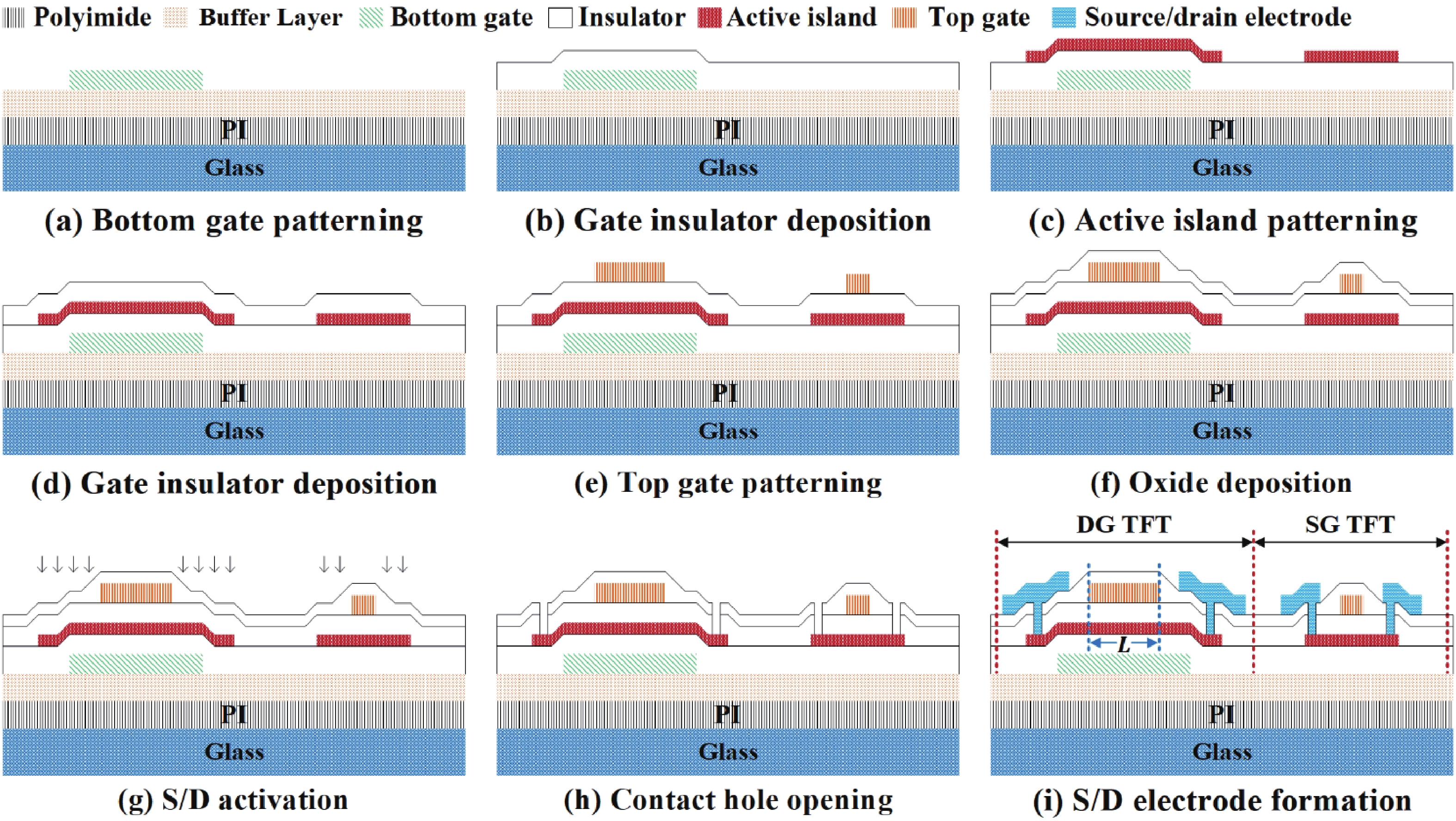
Xia Z H, Lu L, Li J P, et al. Self-aligned elevated-metal metal-oxide thin-film transistors for displays and flexible electronics. 2019 IEEE International Electron Devices Meeting (IEDM), 2020, 8.4. 1 doi: 10.1109/IEDM19573.2019.8993653 |
| [7] |
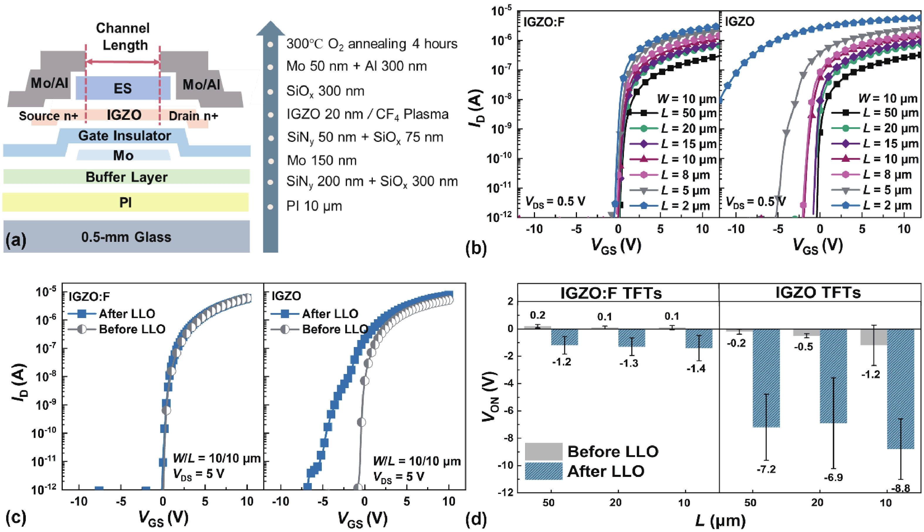
Wang S S, Shi R X, Li J P, et al. Resilience of fluorinated indium-gallium-zinc oxide thin-film transistor against hydrogen-induced degradation. IEEE Electron Device Lett, 2020, 41, 729 doi: 10.1109/LED.2020.2983789 |
| [8] |
Wang Y Q, Jiang W, Xie X Y, et al. A kinetic model for the generation and annihilation of thermally induced carrier donors in a semiconducting metal-oxide thin film. Small, 2022, 18, 2203346 doi: 10.1002/smll.202203346 |
| [9] |
Lu L, Xia Z H, Li J P, et al. A comparative study on fluorination and oxidation of indium–gallium–zinc oxide thin-film transistors. IEEE Electron Device Lett, 2018, 39, 196 doi: 10.1109/LED.2017.2781700 |
| [10] |
Li J P, Lu L, Feng Z Q, et al. An oxidation-last annealing for enhancing the reliability of indium-gallium-zinc oxide thin-film transistors. Appl Phys Lett, 2017, 110, 142102 doi: 10.1063/1.4979649 |
| [11] |
Wang S S, Shi R X, Li J P, et al. 24-2: Distinguished student paper: Fluorination for enhancing the resistance of indium-gallium-zinc oxide thin-film transistor against hydrogen-induced degradation. SID Symp Dig Tech Pap, 2020, 51, 347 doi: 10.1002/sdtp.13875 |
| [12] |
Myny K. The development of flexible integrated circuits based on thin-film transistors. Nat Electron, 2018, 1, 30 doi: 10.1038/s41928-017-0008-6 |
| [13] |
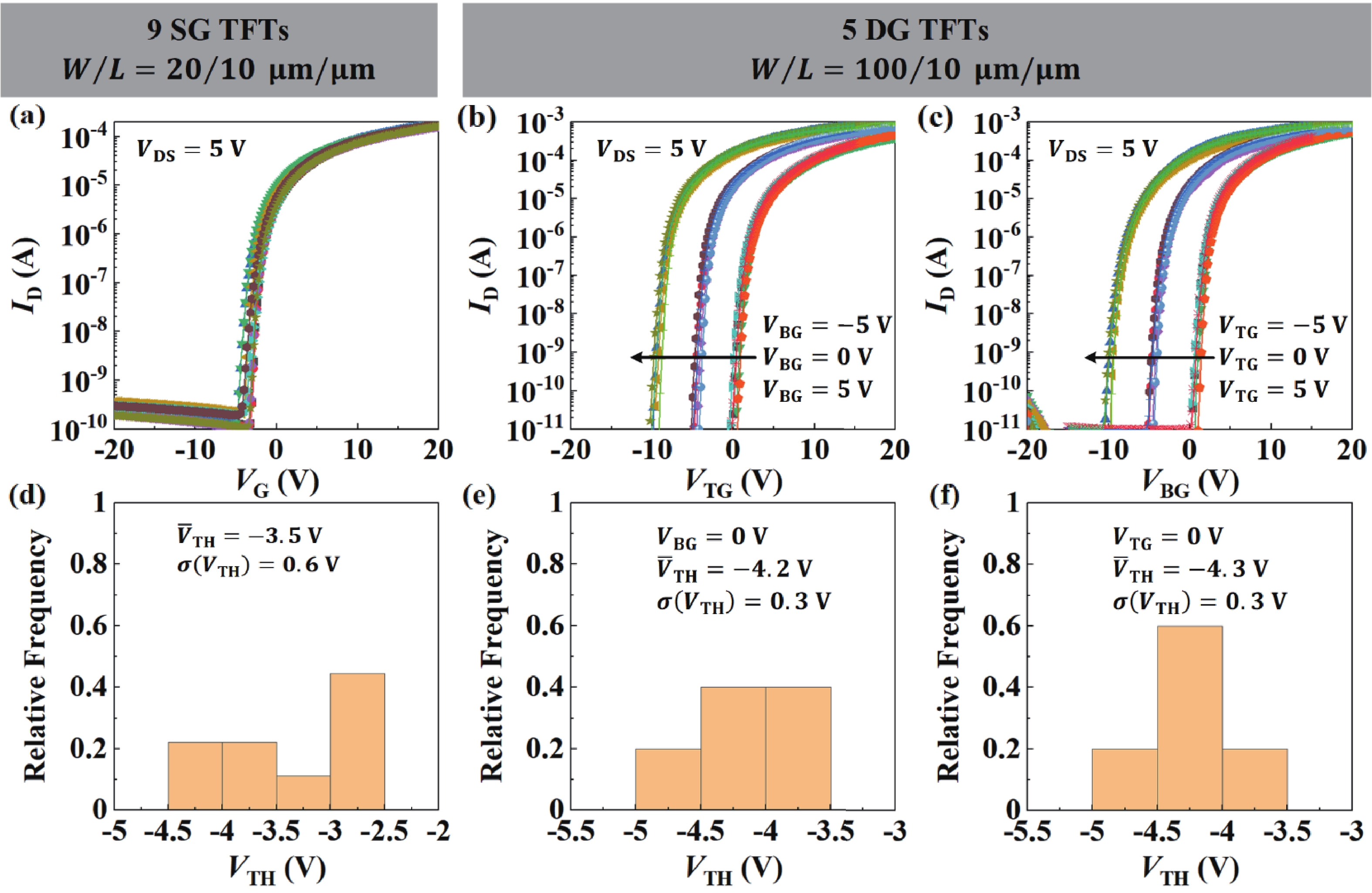
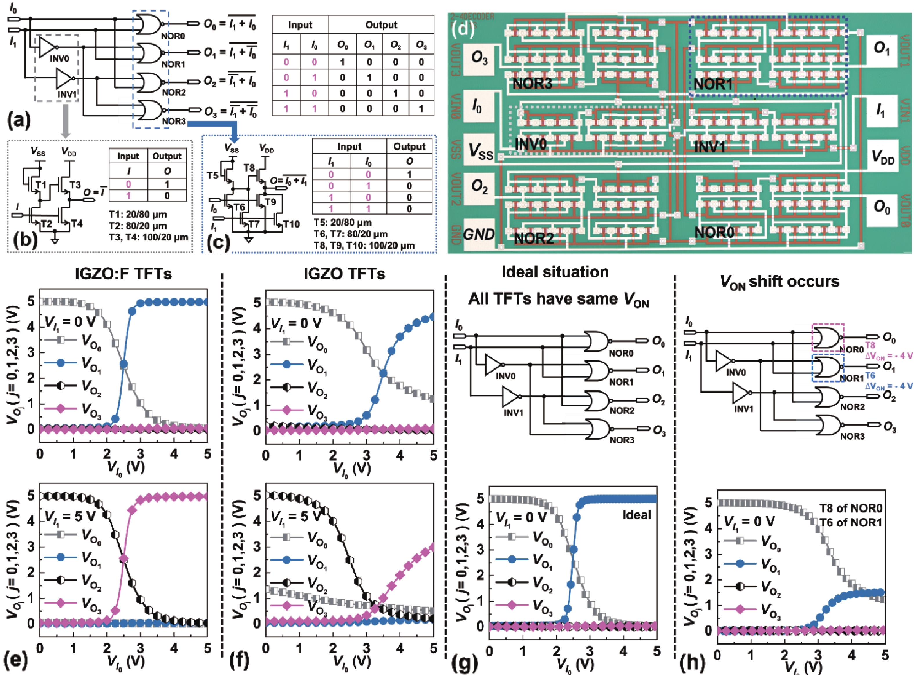
Spijkman M J, Myny K, Smits E C P, et al. Dual-gate thin-film transistors, integrated circuits and sensors. Adv Mater, 2011, 23, 3231 doi: 10.1002/adma.201101493 |
| [14] |
Lei T, Shao L L, Zheng Y Q, et al. Low-voltage high-performance flexible digital and analog circuits based on ultrahigh-purity semiconducting carbon nanotubes. Nat Commun, 2019, 10, 1 doi: 10.1038/s41467-018-07882-8 |
| [15] |
Liu F Y, Liu Z H, Gao S Y, et al. Polyimide film with low thermal expansion and high transparency by self-enhancement of polyimide/SiC nanofibers net. RSC Adv, 2018, 8, 19034 doi: 10.1039/C8RA02479K |
| [16] |
Yung K C, Zeng D W, Yue T M. XPS investigation of Upilex-S polyimide ablated by 355 nm Nd: YAG laser irradiation. Appl Surf Sci, 2001, 173, 193 doi: 10.1016/S0169-4332(00)00884-9 |
| [17] |
Shi R X, Wang S S, Xia Z H, et al. Fluorinated metal-oxide thin-film transistors for circuit implementation on a flexible substrate. IEEE J Flex Electron, 2022, 1, 58 doi: 10.1109/JFLEX.2021.3140044 |
| [18] |
Lu L, Li J P, Kwok H S, et al. High-performance and reliable elevated-metal metal-oxide thin-film transistor for high-resolution displays. 2016 IEEE International Electron Devices Meeting (IEDM), 2017, 32.2. 1 doi: 10.1109/IEDM.2016.7838526 |
| [19] |
Xie X, Chen K, Zhou Z, et al. Conductive indium-tin-zinc-oxide formed using an oxygen plasma treatment through a silicon oxide cover layer. in Digest Tech. Papers SID'23 Conference, 2023.
|
| [20] |
Huang T C, Fukuda K, Lo C M, et al. Pseudo-CMOS: A design style for low-cost and robust flexible electronics. IEEE Trans Electron Devices, 2011, 58, 141 doi: 10.1109/TED.2010.2088127 |
| [21] |
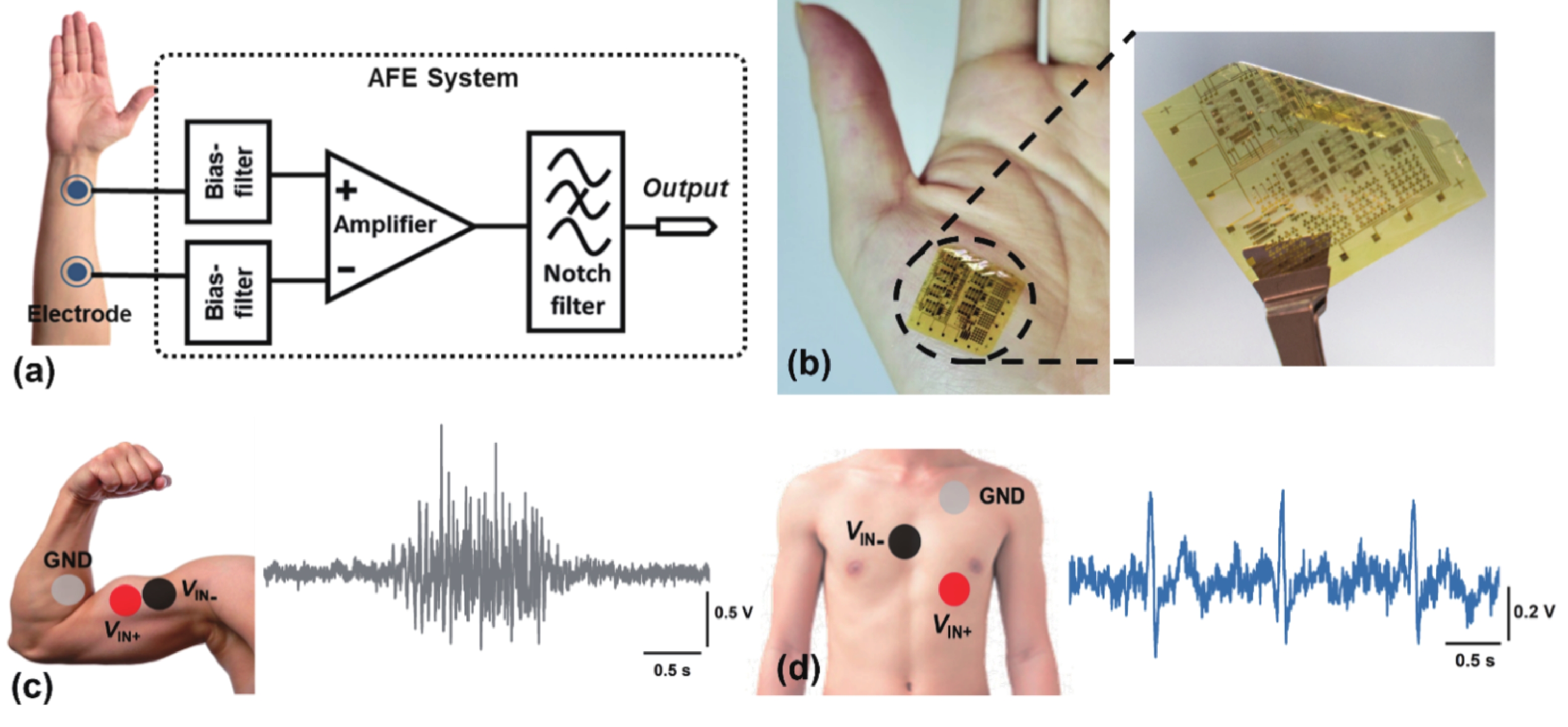
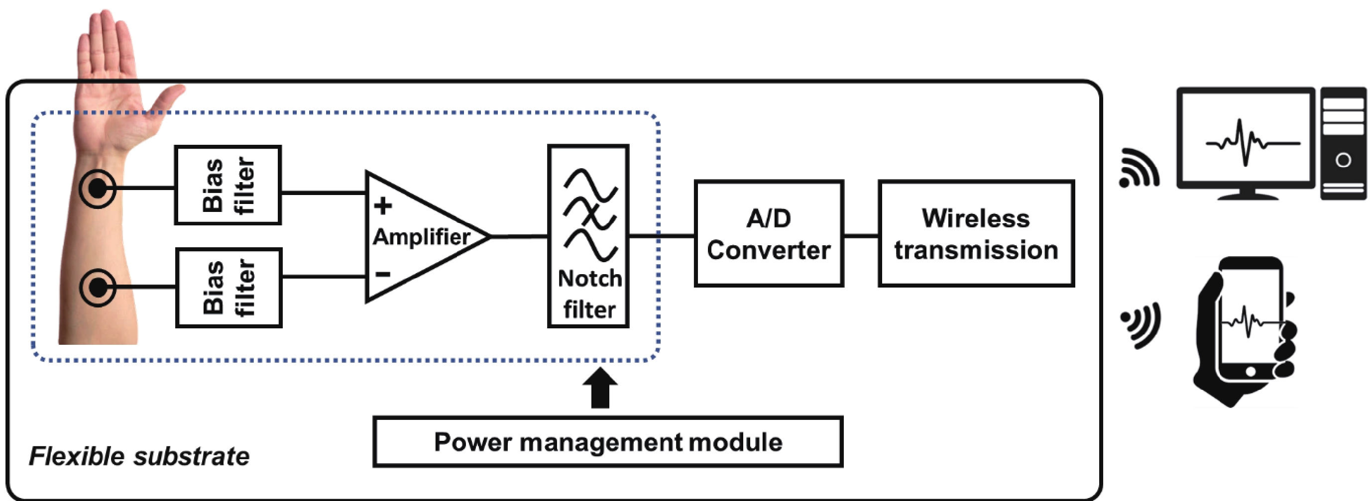
Shi R X, Liu X C, Lei T T, et al. An integrated analog front-end system on flexible substrate for the acquisition of bio-potential signals. Adv Sci, 2023, 10, 2207683 doi: 10.1002/advs.202207683 |
| [22] |
Lei T, Hu Y, Xie X, et al. An active-matrix piezoelectric tactile sensor array with in-pixel amplifier and non-uniformity compensation. in Digest Tech. Papers Transducers'23 Conference, 2023.
|
| [23] |
Lei T T, Hu Y S, Wong M. Active-matrix tactile sensor array based on the monolithic integration of pvdf and dual-gate transistors. 2022 IEEE 35th International Conference on Micro Electro Mechanical Systems Conference (MEMS), 2022, 71 doi: 10.1109/MEMS51670.2022.9699743 |


 DownLoad:


 Runxiao Shi:received his BE degree from Southeast University in 2017 and ME degree from Waseda University in 2018. He is currently working toward a PhD degree with the Department of Electronic and Computer Engineering, The Hong Kong University of Science and Technology. His research interests include flexible indium-gallium-zinc–oxide thin-film transistors and circuits based on metal–oxide TFTs
 Tengteng Lei:got her BS degree from Sun Yat-sen University in 2017 and MS degree from Peking University in 2020. She is currently a PhD student at the State Key Laboratory of Advanced Displays and Optoelectronics Technologies of The Hong Kong University of Science and Technology under the supervision of Prof. Man Wong. Her research interests include metal–oxide thin-film transistors, thin-film integrated circuit design, and tactile sensor arrays
 Zhihe Xia:received a PhD degree from the Department of Electronic and Computer Engineering, The Hong Kong University of Science and Technology, Hong Kong, in 2019. His current research interests include novel metal–oxide thin-film transistors with advanced devices and flexible electronics
 Man Wong:received a PhD degree in electrical engineering from the Center for Integrated Systems, Stanford University, Palo Alto, CA, USA. Since 1992, he has been a faculty member at the Department of Electrical and Electronic Engineering of The Hong Kong University of Science and Technology, Hong Kong


