J. Semicond. > 2023, Volume 44 > Issue 9 > 092602

ARTICLES

Low-temperature conformal vacuum deposition of OLED devices using close-space sublimation

Bryan Siu Ting Tam1, Shou-Cheng Dong1, 2, and Ching W. Tang1, 2

+ Author Affiliations

 Corresponding author: Shou-Cheng Dong, scdong@ust.hk

DOI: 10.1088/1674-4926/44/9/092602

PDF

Turn off MathJax

Abstract: Close-space sublimation (CSS) has been demonstrated as an alternative vacuum deposition technique for fabricating organic light-emitting diodes (OLEDs). CSS utilizes a planar donor plate pre-coated with organic thin films as an area source to rapidly transfer the donor film to a device substrate at temperatures below 200 °C. CSS is also conformal and capable of depositing on odd-shaped substrates using flexible donor media. The evaporation behaviors of organic donor films under CSS were fully characterized using model OLED materials and CSS-deposited films exhibited comparable device performances in an OLED stack to films deposited by conventional point sources. The low temperature and conformal nature of CSS, along with its high material utilization and short process time, make it a promising method for fabricating flexible OLED displays.

Key words: close-space sublimationOLEDthin filmlow temperaturevacuum deposition

Organic light-emitting diode (OLED) displays are currently primarily fabricated by line-of-sight vacuum thermal evaporation (VTE), along with a fine metal mask (FMM) for patterning RGB subpixels side-by-side. Despite being widely utilized by OLED panel makers, the VTE process remains a high-cost production. The VTE sources used in the industry, such as point and linear sources, are typically operated at temperatures higher than 300 °C and need to be placed away from the device substrate to ensure uniformity over large areas, and reduce thermal stress on the substrate and FMM, leading to low material utilization and long deposition time. With the increase in substrate size in mass production, it is imperative to develop alternative cost-effective deposition methods for OLED manufacturing.

Among the numerous approaches that have been proposed to resolve VTE’s drawbacks, close-space sublimation (CSS), which uses a planar donor plate pre-coated with materials as area evaporation sources, offers a promising and practical method for OLED fabrication. Like VTE, CSS is a physical vapor deposition method that operates in a vacuum, which is free of problems associated with solvents in solution processes such as inkjet printing. Unlike conventional VTE processes, CSS has a donor plate that is placed in proximity to the substrate, usually by only a few millimeters to close contact. This close-space configuration makes CSS a conformal deposition process with an extremely high material utilization rate and less shadowing effect when used with shadow masks[14]. Several variants of CSS, such as laser-induced thermal imaging (LITI)[57] and radiation-induced sublimation transfer (RIST)[811], have been studied as alternative methods for producing OLED displays on large substrates. However, these approaches were more focused on the pattern-wise deposition of color pixels that require the donor to be in direct contact with the substrate, causing difficulties in their manufacture and eventual abandonment. In addition, they did not capitalize on another major advantage of CSS, which is the reduced evaporation temperature of donor films compared to bulk materials. In our previous work, we preliminarily showcased the utility of CSS and applied it in depositing the emitting layer of OLEDs without host-dopant segregations [1216].

In this work, we investigated the process characteristics, evaporation behaviors of archetypical OLED materials in CSS, and the properties of CSS-deposited films in detail, and demonstrated CSS as a general conformal deposition process for producing OLED devices at low temperatures. Two heating mechanisms, Joule heating and radiation heating, and two CSS donor media, one flexible and one rigid, were utilized to study CSS profiles and device fabrication. We fully demonstrated the advantages of CSS and identified key factors affecting the performance of thin films and OLED devices fabricated by CSS.

The schematic process flow of CSS used in this study is illustrated in Fig. 1. An organic donor film is deposited on a planar donor plate by a point source. The coated donor is then transferred to a dedicated vacuum chamber and placed at millimeter distances to a device substrate with the donor film facing the substrate. During CSS, the donor plate is flash heated to the film’s evaporation temperature in seconds by Joule heating or irradiation, depending on the material of the donor plate, and deposits the donor film onto the substrate. With the donor preparation arranged offline and orthogonal to the CSS transfer, the deposition of multilayer stacks can be a continuous, in-line process.

Fig. 1.  (Color online) Process flow of CSS.

Each step of CSS is versatile and adaptable to different scenarios. For example, the donor film can be prepared by solution processes, such as inkjet printing, spin coating, and slot-die coating. Counterintuitively, VTE may be a more practical method for donor deposition because it is free of solution-related complications and can utilize existing manufacturing facilities. Since there is no concern of thermal stress or shadowing effect on the donor film, VTE sources can be placed very close to the donor plate and operated at high evaporation rates during donor preparation, ensuring material utilization and deposition speed. For these reasons, we chose VTE for donor preparation in this study. The donor-substrate configuration is also not limited to horizontal. As long as the donor faces the substrate, the assembly’s orientation does not matter. Reversing the position of the donor and the substrate or placing them vertically produced the same deposition result. Since the throw distance of CSS is only a few millimeters, it is less sensitive to the chamber vacuum level that determines the mean free path of vaporized molecules. The CSS of organic films can be performed without difficulty, even at pressures above 10-4 Torr, which is two orders of magnitude higher than the pressure normally required by VTE sources.

The key parameters of this CSS process are the donor material and its heating conditions. The donor plate should have a small thermal mass to enable it to heat quickly. It should also be chemically inert, thermally stable, and mechanically robust for reusability and easy handling. Based on these criteria, we chose two donor media, a flexible tantalum (Ta) foil (10 µm), which can be electrically heated, and a silicon wafer (200 µm), which absorbs light well from a halogen lamp. Each has its own advantages and will be discussed in the following sections.

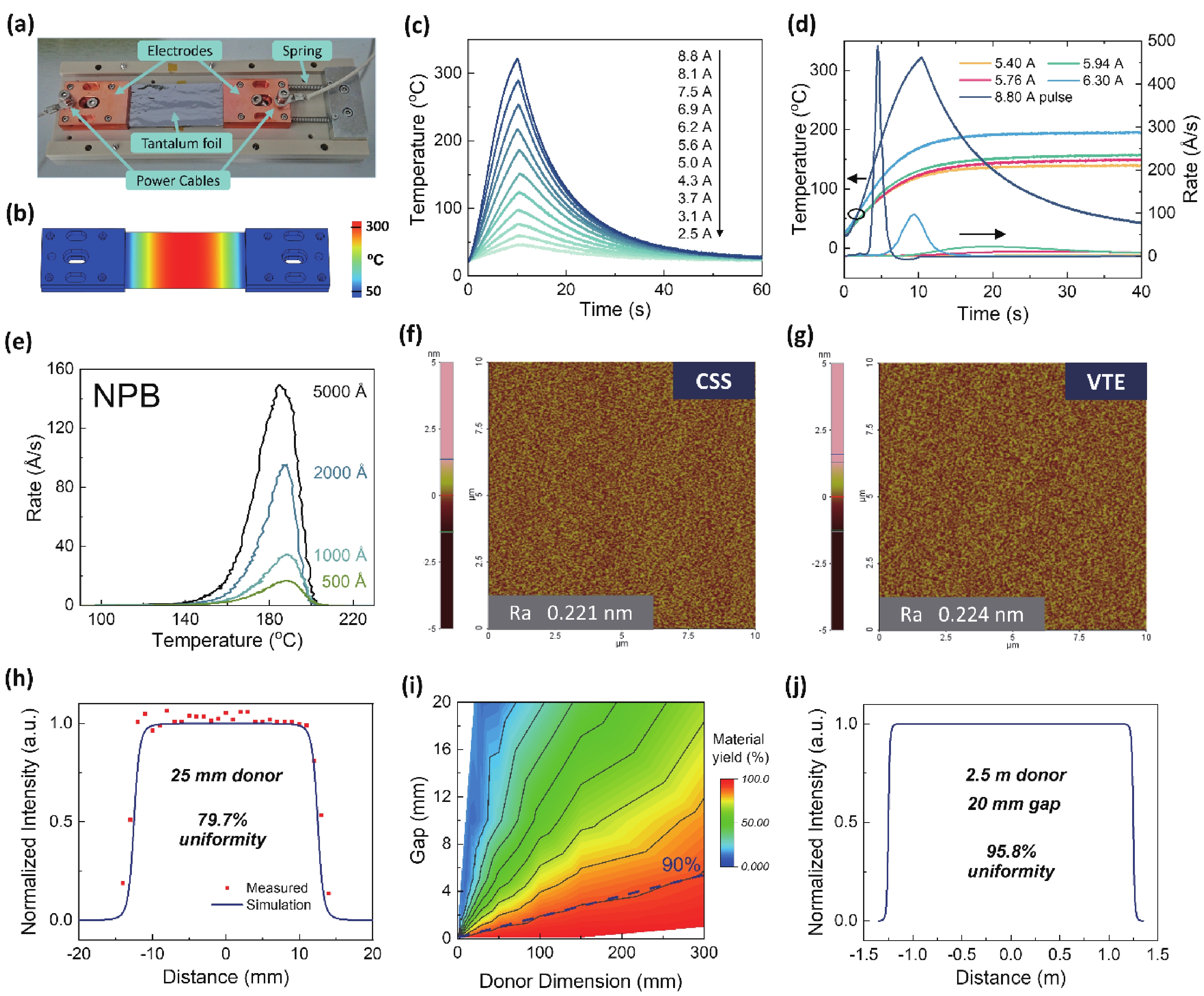
The electrical heating setup for Ta foils is shown in Fig. 2(a). Based on our previous studies[1214], we selected Ta foil as the heating element due to its thermal stability and fast response to current. A 10 µm Ta foil is clamped and tensioned between two copper (Cu) electrodes. The foil temperature can easily be controlled by tuning the current passing through. The foil area between electrodes is 30 × 60 mm2, but the area with uniform temperature distribution is smaller due to the large thermal mass of the Cu electrodes. According to our measurements and simulation (Fig. 2(b)), an area of about 30 × 30 mm2 in the center of the foil is uniformly heated. The donor film will be deposited within this area for CSS. The temporal profiles of the temperature at the center of the foil under different direct currents are measured by a thermocouple and plotted in Fig. 2(c). At a fixed 10 s heating time, the temperature ramp can be finely controlled by the current with the highest temperature reaching above 300 °C using a current of 8.8 A. This temperature is high enough to evaporate most of the OLED materials that we have used. The foil returned to room temperature in about 50 s under vacuum. If a constant current is used, the foil temperature is eventually saturated after 20 s, reaching thermal equilibrium, as shown in Fig. 2(d).

Fig. 2.  (Color online) (a) CSS setup using an electrically heated Ta foil; (b) simulated temperature distribution of the Ta foil under constant current; (c) foil temperatures under different currents with 10 s heating time; (d) the temporal profile of the evaporation rate and Ta foil temperature; (e) CSS evaporation rate of NPB films of various thicknesses from 50 to 500 nm as a function of Ta foil temperatures; (f) AFM image of a CSS-deposited NPB thin film; (g) AFM image of a VTE-deposited NPB film; (h) simulated and measured thickness profile of a CSS-deposited film from a 25 mm donor at a 1 mm gap; (i) film uniformity dependence on the donor-substrate gap and the donor dimensions; and (j) simulated thickness profile of a CSS-deposited film from a 2.5 m donor at a 20 mm gap.

By adjusting the heating profile, the deposition rate in CSS can be controlled in a wide range. We used NPB, an archetypical OLED material, as our model donor film for evaporation studies. A 100 nm NPB film (15 mm in diameter) was deposited in the center of the Ta foil, and a quartz crystal microbalance (QCM) was positioned 5 mm directly above the NPB film to monitor the evaporation rate during CSS at a pressure of 10-6 Torr. The rate profiles under different heating conditions are plotted as a function of time in Fig. 2(d). Rates from only a few angstroms per second (Å/s), similar to those used in VTE, to almost 500 Å/s can be achieved by varying the current applied. Table 1 summarizes the peak deposition rates and corresponding temperatures. Under all of the heating conditions that we tested, the 100 nm NPB film completely evaporated under 200 °C, which is significantly lower than the evaporation temperature of bulk NPB[17]. The rate in CSS is also sensitive to even a small change in donor temperatures. Joule-heating CSS uses significantly less energy than a conventional point source. For depositing a 100 nm film, the power consumption of the Ta foil (20 W with 10 s on time) is about 200 J. In comparison, a typical point source requires well over 2000 J for depositing the same thickness.

Table 1.  Peak temperatures and evaporation rates in CSS at different currents.
Current (A)Peak rate (Å/s)Tpeak (°C)
5.40293
5.7610142
5.9430150
6.30100166
8.80489162
DownLoad: CSV  | Show Table

To gain a better understanding of the evaporation process, we recorded the detailed CSS profile of NPB films of various thicknesses at a slow, fixed heating rate of 1 °C/s and plotted it as a function of foil temperatures. As shown in Fig. 2(e), the NPB film started to evaporate at a very low temperature of around 120 °C, with its rate increasing near exponentially as the temperature rose. The rate peaked at around 187 °C and then dropped sharply due to the depletion of the film. Surprisingly, the temperature at the maximum rate remains the same for donor films of different thicknesses, and the maximum rate is proportional to the film thickness, suggesting that the NPB molecules evaporated from the bulk of the film instead of just from the surface. The increased surface area of the thin film and its amorphous state, both of which lower the intermolecular force, are likely the cause of the low-temperature deposition. The much-reduced evaporation temperatures and shortened process time in CSS significantly lower thermal stress on OLED materials and the chance of thermal decomposition.

The high evaporation rate in CSS, however, raises concerns about morphological issues in transferred films. The AFM image of an NPB film deposited at 500 Å/s peak rate in CSS (1 mm donor-substrate spacing, 10 s heating time) revealed that it actually has the same surface roughness and microscopic morphologies as a typical film deposited at 1 Å/s by a point source, as shown in Figs. 2(f) and 2(g). The macroscopic morphology of CSS-deposited films, characterized by their area uniformity, is also investigated. We simulated the thickness profile of CSS-deposited films assuming that the planar CSS donor film consists of a finite number of Knudsen cells with a plume shape following the cosine law. The solid-blue line in Fig. 2(h) is the calculated thickness profile of a CSS-deposited film using a 25 mm wide donor film at a 1 mm donor-substrate gap. This result was further validated by the measured film thicknesses (red dots in Fig. 2(h)) at different locations of an actual CSS-deposited film under the same conditions. The film uniformity, defined as the percentage of film area within ± 5% non-uniformity, is about 80%. Using this model, the relationship among the donor dimension, the donor-substrate gap, and the uniformity can be established (Fig. 2(i)). Maintaining the ratio between the donor size and the donor-substrate gap above 53 will lead to uniformity higher than 90%. By extrapolation, a donor film of 2.5 m, the size of a Gen 8.5 mother glass, can achieve uniformity of over 95% at a gap of 20 mm, as shown in Fig. 2(j), and a near unity uniformity if the gap is reduced to 1 mm, making CSS a truly conformal deposition method.

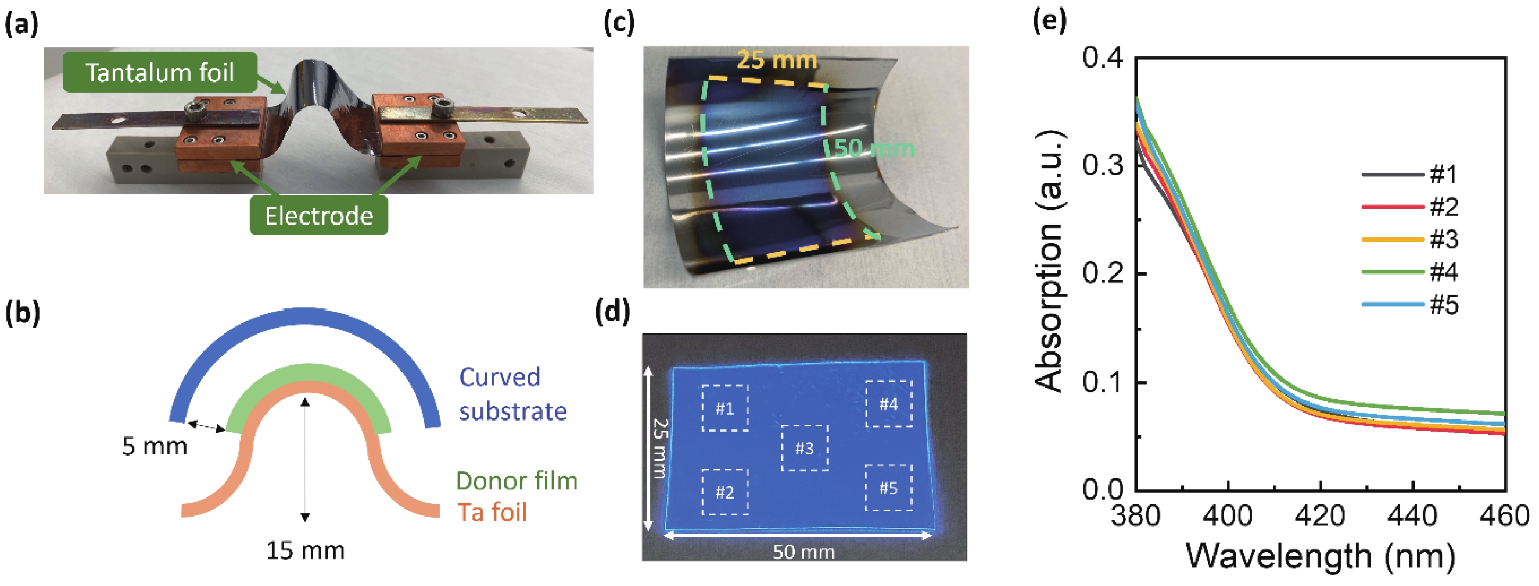
The flexible Ta foil makes it possible to achieve conformal deposition, not only on regular flat substrates but also on odd-shaped objects by conforming the foil to the object’s surface topology. As a proof of concept, we demonstrated CSS deposition on curved surfaces of a rigid stainless-steel piece and flexible PMMA substrates, using Ta foils as the donor media. After depositing an NPB film (30 × 50 mm2, 100 nm thick) on a flattened Ta foil (30 × 60 mm2), the foil was then shaped to conform to the curved steel piece (40 × 55 mm2, r = 18 mm) by varying the distance of terminal Cu electrodes, as illustrated in Figs. 3(a) and 3(b). The gap between the foil and the substrate was kept at about 5 mm. Fig. 3(c) shows the NPB film transferred to a stainless-steel substrate. The mostly uniform interference color suggests excellent film uniformity on the curved surface. The conformal deposition was also demonstrated on a piece of PMMA (25 × 50 mm2) by laminating the PMMA on the stainless-steel piece during CSS. Fig. 3(d) is the fluorescent image of the CSS-deposited NPB film on PMMA. We measured the UV-Vis absorption spectra at five locations on the film. The overlapping spectra indicate similar thickness at these locations, validating the utility of CSS in conformal deposition on curved surfaces.

Fig. 3.  (Color online) (a) CSS using a curved Ta foil; (b) schematics of CSS deposition on curved surfaces; (c) CSS-deposited NPB film on a curved stainless-steel piece; (d) fluorescent image of CSS-deposited NPB on PMMA; and (e) UV-Vis absorption spectra of CSS-deposited NPB at different locations of the PMMA substrate.

The joule-heating CSS scheme is particularly useful in studying the detailed CSS process and specialized deposition scenarios, such as on odd-shaped samples. However, it is limited in large-scale production due to the difficulty in tensioning a donor over large areas. To demonstrate the scalability of CSS, we developed a radiation-heating CSS setup using halogen lamps as the heating source and a silicon wafer (200 µm) as an absorptive donor plate, as shown in Figs. 4(a) and 4(b). Both the silicon donor and the lamp module are easily scalable. The Si donor we used to fabricate CSS devices is 38 × 38 mm2 (1.5’’) and can be extended to 150 × 150 mm2 (6’’). Further scaling can be realized by stitching 6’’ wafers on a carrier. The heating rate is easily adjustable by modulating the lamp power. A typical heating rate of 50 °C/s, comparable to that of Joule heating, can be achieved for the 1.5’’ Si donor using a 250 W halogen bulb (Fig. 4(c)).

Fig. 4.  (Color online) (a) Radiation-heating CSS setup using a halogen bulb for device fabrication; (b) large-area radiation-heating CSS apparatus with a halogen lamp module; and (c) heating profile of the setup in (a) with a 250 W halogen bulb.

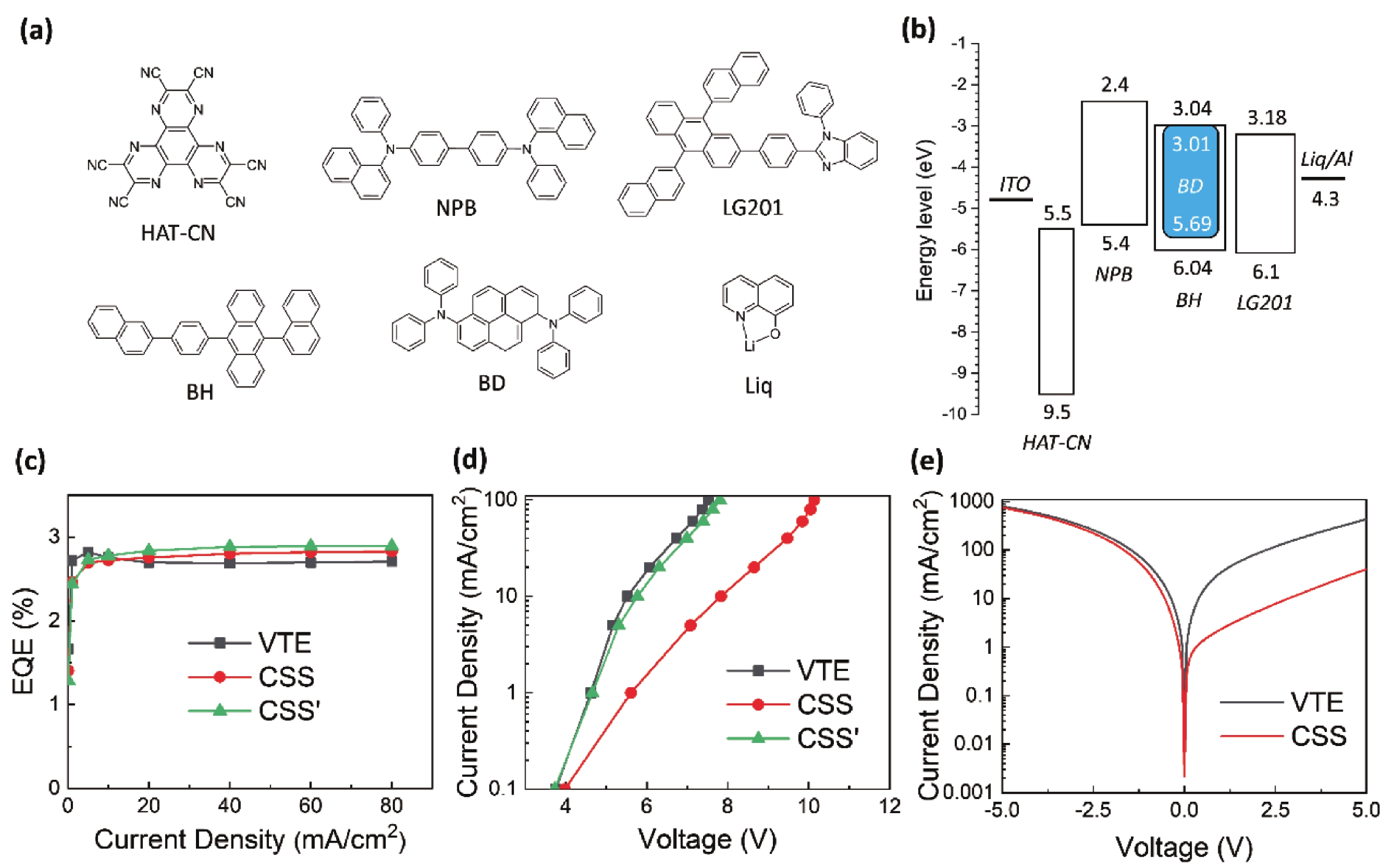
This radiation heating scheme preserved CSS’s high deposition rate and excellent thin-film uniformity. More importantly, the lamp modules can be easily integrated into our OLED coater for device fabrication. We used the following device structure for device performance evaluation: ITO/HAT-CN (10 nm)/NPB (50 nm)/BH:7 wt% BD (30 nm)/LG201 (40 nm)/Liq (2 nm)/Al (100 nm). For simplicity, only the NPB layer was deposited by CSS, with all other layers deposited by point sources. HAT-CN was first deposited on an ITO substrate before being transferred to a dedicated CSS chamber without breaking the vacuum. The substrate was kept at 1 mm atop a preloaded Si donor coated with 50 nm NPB film by a point source. The halogen lamp (Fig. 4(a)) was turned on for 5 s to complete the CSS deposition, and the substrate was immediately moved away from the donor to avoid residue heating and transferred to other chambers for depositing rest layers. The materials used, the device energy diagram, and the device performances are summarized in Fig. 5. A VTE device fabricated completely using point sources was used as a reference.

Fig. 5.  (Color online) (a) The molecular structure of materials used for device fabrication; (b) device energy diagrams; (c) EQE vs. current density and (d) current density vs. voltage of blue OLEDs using CSS- and VTE-deposited NPB layers; and (e) current density vs. voltage plot of hole-only devices.

The CSS device shows near identical EL spectra and similar external quantum efficiencies (EQEs) as the VTE reference, with slightly higher EQEs at current densities larger than 20 mA/cm2 (Fig. 5(c)). However, the driving voltage of the CSS device is significantly higher than the reference, climbing to 8 V at around 10 mA/cm2, which is 3V higher than the VTE device (Fig. 5(d)). According to the device energy diagram, the charge recombination zone of this device is confined to the interface between NPB and the emitting layer. The unaffected EQE and increased voltage suggest that CSS did not introduce additional quenching species at this interface but resulted in a high injection barrier or lowered carrier mobility in the NPB layer.

To identify the cause of this phenomenon, we fabricated a hole-only device using CSS-deposited NPB, following a layer structure of ITO/HAT-CN (10 nm)/NPB (100 nm)/HAT-CN (10 nm)/Al (100 nm). The device was swept using both forward and reversed bias, as shown in Fig. 5(e). Only the forward scan exhibited lowered current densities than a VTE reference at the same voltages, indicating that the mobility in the bulk of CSS-deposited NPB is unaffected but there is a higher injection barrier at the first HAT-CN/NPB interface. We have previously reported that the moisture adsorbed on the CSS donor plate may contaminate the device and cause performance deterioration[15]. The donor in this study also experienced a brief air exposure between the preparation and loading steps, leaving the CSS device vulnerable to atmospheric contaminants on the HAT-CN surface incorporated during the CSS process. To fix this issue, we deposited a 5 nm NPB layer on the HAT-CN layer by a point source before the CSS of NPB to isolate contaminants from the interface. The resulting device, denoted as CSS’, immediately showed recovered driving voltage like the reference and higher efficiency than the previous CSS device, which validates our hypothesis. We anticipate that such an exposure problem will be completely resolved using a better-controlled process, such as in situ donor preparation and handling without breaking the vacuum, which would eliminate the need for additional VTE-deposited NPB layers.

We have developed a low-temperature conformal CSS deposition processes for fabricating OLED devices. Two CSS schemes, one using Joule-heating of Ta foil and the other using radiation-heating of Si wafers, have been evaluated for thin-film deposition and device fabrication. We demonstrated that CSS could achieve conformal deposition of organic thin films with high uniformity at temperatures lower than 200 °C within seconds. Our study showed that CSS could produce thin films of comparable device performance with those prepared by conventional VTE techniques. We believe that CSS is readily applicable to all organic layers of the OLED stack. With the use of flexible donor media, CSS can even deposit conformally on odd-shaped substrates, a feat that is unmatched by other deposition methods and is potentially useful for fabricating flexible electronics.

This work was financially supported by the General Research Fund (16309918) from the Research Grant Council, Hong Kong, and funding from the Institute for Advanced Study of the Hong Kong University of Science and Technology.


[1]
Hwang C, Im Y, Kim J J, et al. Plane source evaporation for new patterning technique of high resolution AMOLEDs. IMID 2015 Digest, 2016, 272
[2]
Hwang C, Kim S S, Lee H, et al. Plane source evaporation techniques for super ultra high resolution flexible AMOLED. SID Symp Dig Tech Pap, 2017, 48, 523 doi: 10.1002/sdtp.11690
[3]
Hwang C, Kim S S, Bang S W, et al. Novel plane source FMM evaporation techniques for manufacturing of 2250ppi flexible AMOLEDs. SID Symp Dig Tech Pap, 2018, 49, 1003 doi: 10.1002/sdtp.12222
[4]
Hwang C, Kim S S, Bang S W, et al. Unique belt plane source evaporation techniques for the mass production of 2250ppi AMOLED and 77” QD OLED TV. SID Symp Dig Tech Pap, 2019, 50, 949 doi: 10.1002/sdtp.13082
[5]
Lee S T, Chin B D, Kim M H, et al. A novel patterning method for full-color organic light-emitting devices: Laser induced thermal imaging (LITI). SID Symp Dig Tech Pap, 2004, 35, 1008 doi: 10.1889/1.1821308
[6]
Cho S H, Suh M C, Kim J W. The operating voltage behavior of green fluorescent organic light emitting diode with blue common layer structure during laser imaging process. Org Electron, 2012, 13, 2945 doi: 10.1016/j.orgel.2012.08.013
[7]
Suh M C, Kang T M, Cho S W, et al. 53.2: Invited paper: Large-area color-patterning technology for AMOLED. SID Symp Dig Tech Pap, 2009, 40, 794 doi: 10.1889/1.3256909
[8]
Boroson M, Tutt L, Nguyen K, et al. 16.5L: Late-news-paper: Non-contact OLED color patterning by radiation-induced sublimation transfer (RIST). SID Symp Dig Tech Pap, 2005, 36, 972 doi: 10.1889/1.2036612
[9]
Hirano T, Matsuo K, Kohinata K, et al. 53.2: Distinguished paper: Novel laser transfer technology for manufacturing large-sized OLED displays. SID Symp Dig Tech Pap, 2007, 38, 1592 doi: 10.1889/1.2785623
[10]
Fardel R, Nagel M, Nüesch F, et al. Fabrication of organic light-emitting diode pixels by laser-assisted forward transfer. Applied Physics Letters, 2007, 91, 061103 doi: 10.1063/1.2759475
[11]
Long M, Bruce E K, Neil P R, et al. Enabling high-throughput, low-cost manufacturing of OLED display and lighting panels. MRS Online Proc Libr, 2010, 1212, 706 doi: 10.1557/PROC-1212-S06-06-C07-06
[12]
Tam S T. Organic light emitting diode devices fabricated by close-space sublimation. MPhil Thesis, Hong Kong University of Science and Technology, 2019
[13]
Tam S T. Investigation of organic light-emitting diodes fabricated by close-space sublimation. PhD Thesis, Hong Kong University of Science and Technology, 2022
[14]
Tam S T, Dong S C, Tang C W. Close-space sublimation of OLED materials via electrical heating of metal foils. SID Symp Dig Tech Pap, 2018, 49, 737 doi: 10.1002/sdtp.12830
[15]
Tam B S T, Dong S C, Tang C W. Blue OLEDs fabricated by close-space sublimation. SID Symp Dig Tech Pap, 2019, 50, 153 doi: 10.1002/sdtp.12878
[16]
Dong H J, Tam B S T, Ding L, et al. Low-temperature vacuum deposition of green phosphorescent OLED devices using close-space sublimation of spirobifluorene hosts. J Lumin, 2022, 252, 119360 doi: 10.1016/j.jlumin.2022.119360
[17]
Shim S, Kim J T, Shin E J, et al. Phase behaviors of NPB molecule under vacuum. Mater Res Bull, 2016, 82, 67 doi: 10.1016/j.materresbull.2016.01.054
Fig. 1.  (Color online) Process flow of CSS.

Fig. 2.  (Color online) (a) CSS setup using an electrically heated Ta foil; (b) simulated temperature distribution of the Ta foil under constant current; (c) foil temperatures under different currents with 10 s heating time; (d) the temporal profile of the evaporation rate and Ta foil temperature; (e) CSS evaporation rate of NPB films of various thicknesses from 50 to 500 nm as a function of Ta foil temperatures; (f) AFM image of a CSS-deposited NPB thin film; (g) AFM image of a VTE-deposited NPB film; (h) simulated and measured thickness profile of a CSS-deposited film from a 25 mm donor at a 1 mm gap; (i) film uniformity dependence on the donor-substrate gap and the donor dimensions; and (j) simulated thickness profile of a CSS-deposited film from a 2.5 m donor at a 20 mm gap.

Fig. 3.  (Color online) (a) CSS using a curved Ta foil; (b) schematics of CSS deposition on curved surfaces; (c) CSS-deposited NPB film on a curved stainless-steel piece; (d) fluorescent image of CSS-deposited NPB on PMMA; and (e) UV-Vis absorption spectra of CSS-deposited NPB at different locations of the PMMA substrate.

Fig. 4.  (Color online) (a) Radiation-heating CSS setup using a halogen bulb for device fabrication; (b) large-area radiation-heating CSS apparatus with a halogen lamp module; and (c) heating profile of the setup in (a) with a 250 W halogen bulb.

Fig. 5.  (Color online) (a) The molecular structure of materials used for device fabrication; (b) device energy diagrams; (c) EQE vs. current density and (d) current density vs. voltage of blue OLEDs using CSS- and VTE-deposited NPB layers; and (e) current density vs. voltage plot of hole-only devices.

Table 1.   Peak temperatures and evaporation rates in CSS at different currents.

Current (A)Peak rate (Å/s)Tpeak (°C)
5.40293
5.7610142
5.9430150
6.30100166
8.80489162
DownLoad: CSV
[1]
Hwang C, Im Y, Kim J J, et al. Plane source evaporation for new patterning technique of high resolution AMOLEDs. IMID 2015 Digest, 2016, 272
[2]
Hwang C, Kim S S, Lee H, et al. Plane source evaporation techniques for super ultra high resolution flexible AMOLED. SID Symp Dig Tech Pap, 2017, 48, 523 doi: 10.1002/sdtp.11690
[3]
Hwang C, Kim S S, Bang S W, et al. Novel plane source FMM evaporation techniques for manufacturing of 2250ppi flexible AMOLEDs. SID Symp Dig Tech Pap, 2018, 49, 1003 doi: 10.1002/sdtp.12222
[4]
Hwang C, Kim S S, Bang S W, et al. Unique belt plane source evaporation techniques for the mass production of 2250ppi AMOLED and 77” QD OLED TV. SID Symp Dig Tech Pap, 2019, 50, 949 doi: 10.1002/sdtp.13082
[5]
Lee S T, Chin B D, Kim M H, et al. A novel patterning method for full-color organic light-emitting devices: Laser induced thermal imaging (LITI). SID Symp Dig Tech Pap, 2004, 35, 1008 doi: 10.1889/1.1821308
[6]
Cho S H, Suh M C, Kim J W. The operating voltage behavior of green fluorescent organic light emitting diode with blue common layer structure during laser imaging process. Org Electron, 2012, 13, 2945 doi: 10.1016/j.orgel.2012.08.013
[7]
Suh M C, Kang T M, Cho S W, et al. 53.2: Invited paper: Large-area color-patterning technology for AMOLED. SID Symp Dig Tech Pap, 2009, 40, 794 doi: 10.1889/1.3256909
[8]
Boroson M, Tutt L, Nguyen K, et al. 16.5L: Late-news-paper: Non-contact OLED color patterning by radiation-induced sublimation transfer (RIST). SID Symp Dig Tech Pap, 2005, 36, 972 doi: 10.1889/1.2036612
[9]
Hirano T, Matsuo K, Kohinata K, et al. 53.2: Distinguished paper: Novel laser transfer technology for manufacturing large-sized OLED displays. SID Symp Dig Tech Pap, 2007, 38, 1592 doi: 10.1889/1.2785623
[10]
Fardel R, Nagel M, Nüesch F, et al. Fabrication of organic light-emitting diode pixels by laser-assisted forward transfer. Applied Physics Letters, 2007, 91, 061103 doi: 10.1063/1.2759475
[11]
Long M, Bruce E K, Neil P R, et al. Enabling high-throughput, low-cost manufacturing of OLED display and lighting panels. MRS Online Proc Libr, 2010, 1212, 706 doi: 10.1557/PROC-1212-S06-06-C07-06
[12]
Tam S T. Organic light emitting diode devices fabricated by close-space sublimation. MPhil Thesis, Hong Kong University of Science and Technology, 2019
[13]
Tam S T. Investigation of organic light-emitting diodes fabricated by close-space sublimation. PhD Thesis, Hong Kong University of Science and Technology, 2022
[14]
Tam S T, Dong S C, Tang C W. Close-space sublimation of OLED materials via electrical heating of metal foils. SID Symp Dig Tech Pap, 2018, 49, 737 doi: 10.1002/sdtp.12830
[15]
Tam B S T, Dong S C, Tang C W. Blue OLEDs fabricated by close-space sublimation. SID Symp Dig Tech Pap, 2019, 50, 153 doi: 10.1002/sdtp.12878
[16]
Dong H J, Tam B S T, Ding L, et al. Low-temperature vacuum deposition of green phosphorescent OLED devices using close-space sublimation of spirobifluorene hosts. J Lumin, 2022, 252, 119360 doi: 10.1016/j.jlumin.2022.119360
[17]
Shim S, Kim J T, Shin E J, et al. Phase behaviors of NPB molecule under vacuum. Mater Res Bull, 2016, 82, 67 doi: 10.1016/j.materresbull.2016.01.054
1

High Curie temperature ferromagnetism and high hole mobility in tensile strained Mn-doped SiGe thin films

Jianhua Zhao

Journal of Semiconductors, 2020, 41(8): 080201. doi: 10.1088/1674-4926/41/8/080201

2

Review of recent progresses on flexible oxide semiconductor thin film transistors based on atomic layer deposition processes

Jiazhen Sheng, Ki-Lim Han, TaeHyun Hong, Wan-Ho Choi, Jin-Seong Park, et al.

Journal of Semiconductors, 2018, 39(1): 011008. doi: 10.1088/1674-4926/39/1/011008

3

Substrate temperature dependent studies on properties of chemical spray pyrolysis deposited CdS thin films for solar cell applications

Kiran Diwate, Amit Pawbake, Sachin Rondiya, Rupali Kulkarni, Ravi Waykar, et al.

Journal of Semiconductors, 2017, 38(2): 023001. doi: 10.1088/1674-4926/38/2/023001

4

Zinc-doped CdS nanoparticles synthesized by microwave-assisted deposition

Abideen A. Ibiyemi, Ayodeji O Awodugba, Olusola Akinrinola, Abass A Faremi

Journal of Semiconductors, 2017, 38(9): 093002. doi: 10.1088/1674-4926/38/9/093002

5

A simple chemical route to synthesize the umangite phase of copper selenide (Cu3Se2) thin film at room temperature

Balasaheb M. Palve, Sandesh R. Jadkar, Habib M. Pathan

Journal of Semiconductors, 2017, 38(6): 063003. doi: 10.1088/1674-4926/38/6/063003

6

Temperature sensor based on composite film of vanadium complex (VO2(3-fl)) and CNT

Kh. S. Karimov, M. Mahroof-Tahir, M. Saleem, M. Tariq Saeed Chani, A. Khan Niaz, et al.

Journal of Semiconductors, 2015, 36(7): 073004. doi: 10.1088/1674-4926/36/7/073004

7

Electrical properties of Ge:Ga near the metal-insulator transition

M Errai, A El Kaaouachi, H El Idrissi

Journal of Semiconductors, 2015, 36(6): 062001. doi: 10.1088/1674-4926/36/6/062001

8

Variable range hopping conduction in n-CdSe samples at very low temperature

M Errai, A El Kaaouachi, H El Idrissi

Journal of Semiconductors, 2015, 36(12): 122001. doi: 10.1088/1674-4926/36/12/122001

9

Resistive humidity sensor based on vanadium complex films

Kh. S. Karimov, M. Saleem, M. Mahroof-Tahir, R. Akram, M.T. Saeed Chanee, et al.

Journal of Semiconductors, 2014, 35(9): 094001. doi: 10.1088/1674-4926/35/9/094001

10

Significant improvement of ZnS film electrical and optical performance by indium incorporation

Jinhuo Chen, Wenjian Li

Journal of Semiconductors, 2014, 35(9): 093003. doi: 10.1088/1674-4926/35/9/093003

11

Influence of growth time on crystalline structure, conductivity and optical properties of ZnO thin films

Said Benramache, Foued Chabane, Boubaker Benhaoua, Fatima Z. Lemmadi

Journal of Semiconductors, 2013, 34(2): 023001. doi: 10.1088/1674-4926/34/2/023001

12

Correlation between electrical conductivity-optical band gap energy and precursor molarities ultrasonic spray deposition of ZnO thin films

Said Benramache, Okba Belahssen, Abderrazak Guettaf, Ali Arif

Journal of Semiconductors, 2013, 34(11): 113001. doi: 10.1088/1674-4926/34/11/113001

13

A nanostructured copper telluride thin film grown at room temperature by an electrodeposition method

S. S. Dhasade, S. H. Han, V. J. Fulari

Journal of Semiconductors, 2012, 33(9): 093002. doi: 10.1088/1674-4926/33/9/093002

14

Effect of deposition conditions on the physical properties of SnxSy thin films prepared by the spray pyrolysis technique

M. R. Fadavieslam, N. Shahtahmasebi, M. Rezaee-Roknabadi, M. M. Bagheri-Mohagheghi

Journal of Semiconductors, 2011, 32(11): 113002. doi: 10.1088/1674-4926/32/11/113002

15

Poly-Si Film Functional Layer Based AM-OLED Display Panel

Li Yang, Zhao Shuyun, Wu Chunya, Meng Zhiguo, Wang Yi, et al.

Journal of Semiconductors, 2008, 29(12): 2393-2397.

16

Driving Circuit for AMOLED with Fault Tolerance

Li Dayong, Liu Ming, Wei Wang

Chinese Journal of Semiconductors , 2007, 28(9): 1337-1340.

17

A Testing Method on a Thin Film Transistor Array for Active Matrix Organic Emitting Diode

Liu Xueqiang, Zhang Tong, Wang Lijie, Xia Zhiqiang, Li Mingyou, et al.

Chinese Journal of Semiconductors , 2007, 28(7): 1161-1164.

18

Preparation of Si/SiO2 Optical Thin Film by Double Source Electron Beam Evaporation Technology

Zhao Miao, Zhou Daibing, Tan Manqing, Wang Xiaodong, Wu Xuming, et al.

Chinese Journal of Semiconductors , 2006, 27(9): 1586-1589.

19

Fabrication of a 125mm Poly-Si TFT Active-Matrix Driving Color AMOLED

Meng Zhiguo, Kwok Hoising, Wu Chunya, Wong Man, Xiong Shaozhen, et al.

Chinese Journal of Semiconductors , 2006, 27(8): 1514-1517.

20

实现64级灰度显示的无源OLED驱动芯片的设计

刘铭, 秦波, Xiao Wenyu, Zhong Huiming, Chen Liang, et al.

Chinese Journal of Semiconductors , 2006, 27(11): 1889-1893.

1. Li, D., Xu, H., Li, Y. et al. Valence gradient induced charge transfer enabling efficient hydrogen spillover in hydrogen evolution. Chemical Engineering Journal, 2025. doi:10.1016/j.cej.2024.158734
2. Zhang, X., Zhou, K., Zhao, Z. et al. Printable Photonic Materials and Devices for Smart Healthcare. Advanced Materials, 2025. doi:10.1002/adma.202418729
3. Zhao, J., Lin, R., Wang, J. et al. Ultra-thin size-controllable surface plasmon polariton laser by PDMS-assisted imprinting. Journal of Physics D: Applied Physics, 2024, 57(40): 405102. doi:10.1088/1361-6463/ad5f97
4. Liang, Y., Wang, Z., Shen, G. CMOS-level mega-pixel organic camera chips made of photocrosslinked photovoltaic nanocells. Science China Materials, 2024, 67(9): 3043-3045. doi:10.1007/s40843-024-3050-5
5. Zhang, L., Zhou, R., Ma, W. et al. Junction Piezotronic Transistor Arrays Based on Patterned ZnO Nanowires for High-Resolution Tactile and Photo Mapping. Sensors, 2024, 24(15): 4775. doi:10.3390/s24154775
6. Wan, D., Zhou, J., Meng, G. et al. Peripheral carbazole units-decorated MR emitter containing B−N covalent bond for highly efficient green OLEDs with low roll-off. Journal of Semiconductors, 2024, 45(8): 082402. doi:10.1088/1674-4926/24040008
7. Du, Y., Bai, Y., Cao, W. et al. Research progress on displays and optical adhesives for flexible 3C products. European Polymer Journal, 2024. doi:10.1016/j.eurpolymj.2024.113053
8. Kwok, H.-S., Fan, Z. Preface to Special Issue on Advanced Optoelectronic and Electronic Devices toward Future Displays. Journal of Semiconductors, 2023, 44(9): 090101. doi:10.1088/1674-4926/44/9/090101
  • Search

    Advanced Search >>

    GET CITATION

    Bryan Siu Ting Tam, Shou-Cheng Dong, Ching W. Tang. Low-temperature conformal vacuum deposition of OLED devices using close-space sublimation[J]. Journal of Semiconductors, 2023, 44(9): 092602. doi: 10.1088/1674-4926/44/9/092602
    B S T Tam, S C Dong, C W Tang. Low-temperature conformal vacuum deposition of OLED devices using close-space sublimation[J]. J. Semicond, 2023, 44(9): 092602. doi: 10.1088/1674-4926/44/9/092602
    shu

    Export: BibTex EndNote

    Article Metrics

    Article views: 1171 Times PDF downloads: 105 Times Cited by: 8 Times

    History

    Received: 15 May 2023 Revised: 16 June 2023 Online: Accepted Manuscript: 14 August 2023Uncorrected proof: 15 August 2023Corrected proof: 18 August 2023Published: 10 September 2023

    Catalog

      Email This Article

      User name:
      Email:*请输入正确邮箱
      Code:*验证码错误
      Bryan Siu Ting Tam, Shou-Cheng Dong, Ching W. Tang. Low-temperature conformal vacuum deposition of OLED devices using close-space sublimation[J]. Journal of Semiconductors, 2023, 44(9): 092602. doi: 10.1088/1674-4926/44/9/092602 ****B S T Tam, S C Dong, C W Tang. Low-temperature conformal vacuum deposition of OLED devices using close-space sublimation[J]. J. Semicond, 2023, 44(9): 092602. doi: 10.1088/1674-4926/44/9/092602
      Citation:
      Bryan Siu Ting Tam, Shou-Cheng Dong, Ching W. Tang. Low-temperature conformal vacuum deposition of OLED devices using close-space sublimation[J]. Journal of Semiconductors, 2023, 44(9): 092602. doi: 10.1088/1674-4926/44/9/092602 ****
      B S T Tam, S C Dong, C W Tang. Low-temperature conformal vacuum deposition of OLED devices using close-space sublimation[J]. J. Semicond, 2023, 44(9): 092602. doi: 10.1088/1674-4926/44/9/092602

      Low-temperature conformal vacuum deposition of OLED devices using close-space sublimation

      DOI: 10.1088/1674-4926/44/9/092602
      More Information
      • Bryan Siu Ting Tam:is a Postdoctoral Fellow with the Department of Electronic and Computer Engineering at HKUST. He received his BE in 2017, MPhil in 2019, and PhD in 2022, all from HKUST. His research is focused on deposition and patterning methods for high-resolution OLED displays and the degradation mechanism of blue OLEDs
      • Shou-Cheng Dong:is a Research Assistant Professor with the Department of Electronic and Computer Engineering and an IAS Junior Fellow at HKUST. He received his PhD in 2011 from Wuhan University, China. He conducted postdoctoral research at Soochow University and the City University of Hong Kong before joining HKUST in 2014. His research is focused on blue OLED lifetime deposition and patterning methods for high-resolution OLED displays, and color conversion technologies

      • Ching W. Tang:was the IAS Bank of East Asia Professor at the Hong Kong University of Science and Technology from 2013 to 2023 and the Doris Johns Cherry Professor of Chemical Engineering at the University of Rochester from 2006 to 2013. He is currently an Emeritus Professor at the University of Rochester. Prof Tang received his B.S. from the University of British Columbia and his Ph.D. from Cornell University. Before academia, he spent almost 30 years in the Kodak Research Laboratories in Rochester, NY, where he pioneered the field of organic electronics with the inventions of OLED and OPV. Prof. Tang holds fellowships at many distinguished organizations, such as the U.S. National Academy of Engineering and the Academy of Sciences of Hong Kong. He received numerous prestigious awards for his invention of OLED, including the Kyoto Prize, the Wolf Prize, and the SID Fellow. His recent research has been focused on OLED lifetime and fabrication techniques for high-resolution OLED displays
      • Corresponding author: scdong@ust.hk
      • Received Date: 2023-05-15
      • Revised Date: 2023-06-16
      • Available Online: 2023-08-14

      Catalog

        /

        DownLoad:  Full-Size Img  PowerPoint
        Return
        Return