


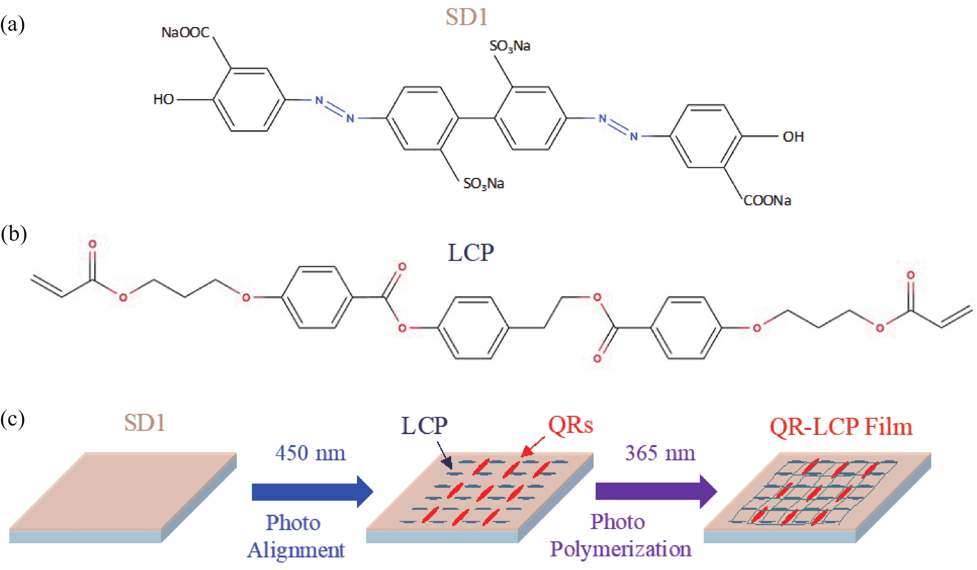
Fig. 1.
(Color online) Photo-induced QRs alignment. Chemical structure of (a) SD1 and (b) LCP. (c) Process flow for unidirectional QRs alignment.
ARTICLES
Wanlong Zhang1, , Julian Schneider3, Maksym F. Prodanov2, Valerii V. Vashchenko2, Andrey L. Rogach3, Xiaocong Yuan1 and Abhishek K. Srivastava2,
Corresponding author: Wanlong Zhang, zwl@szu.edu.cn; Abhishek K. Srivastava, eeabhishek@ust.hk
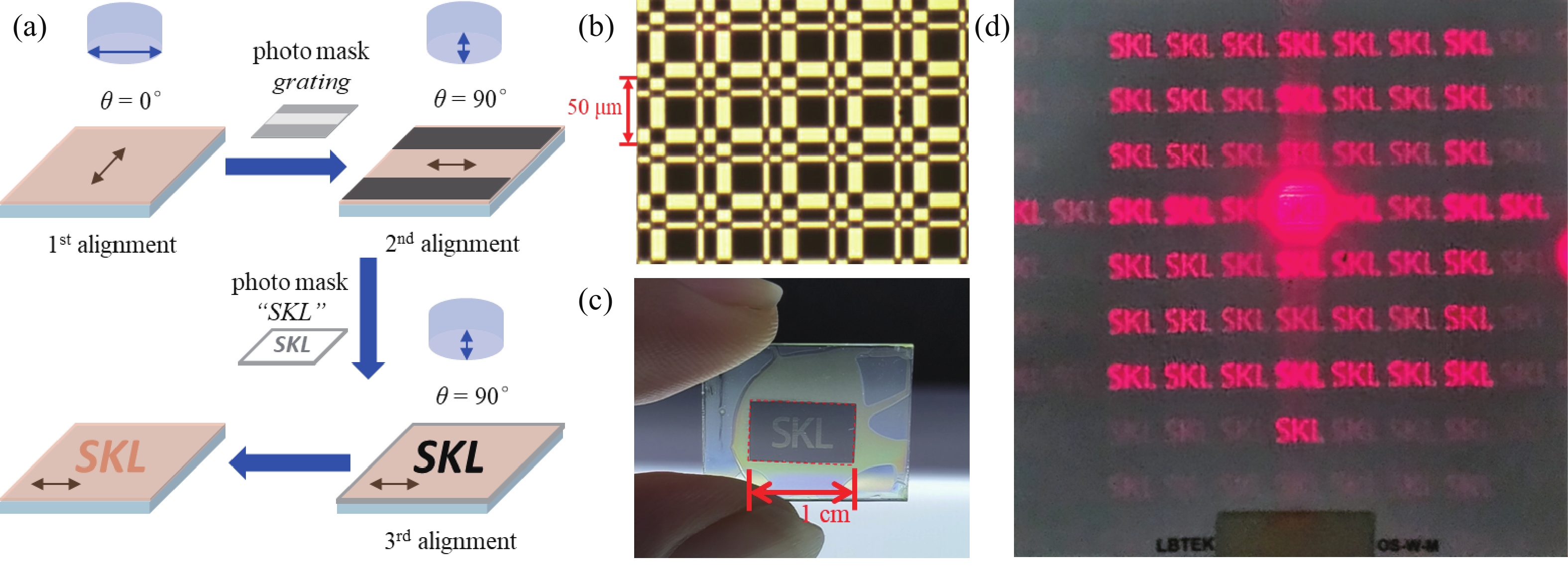
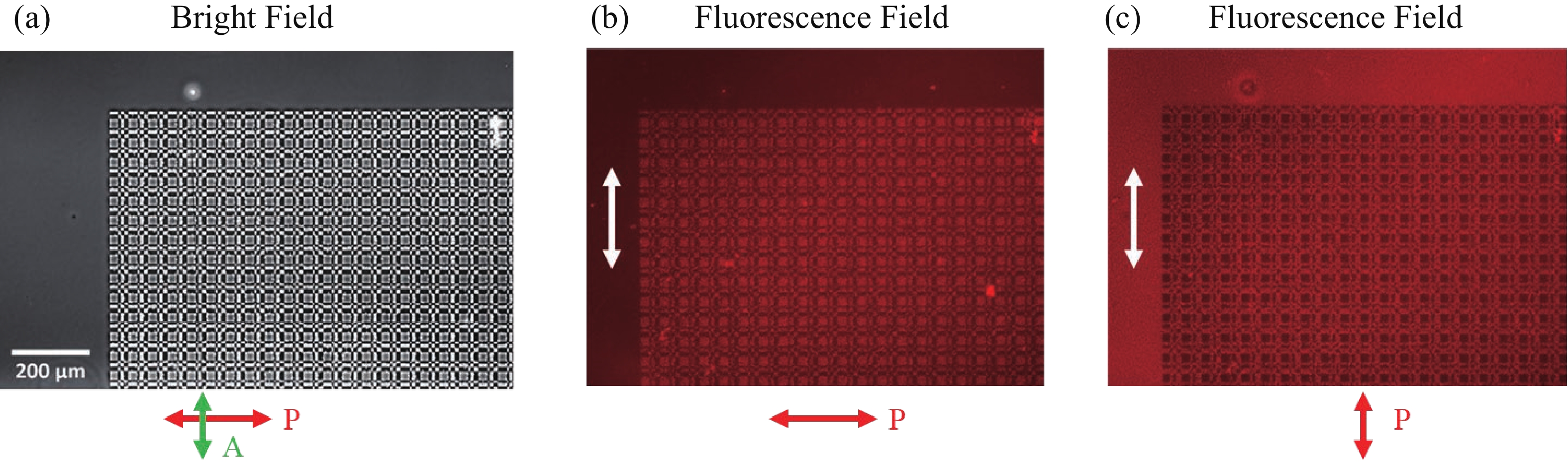
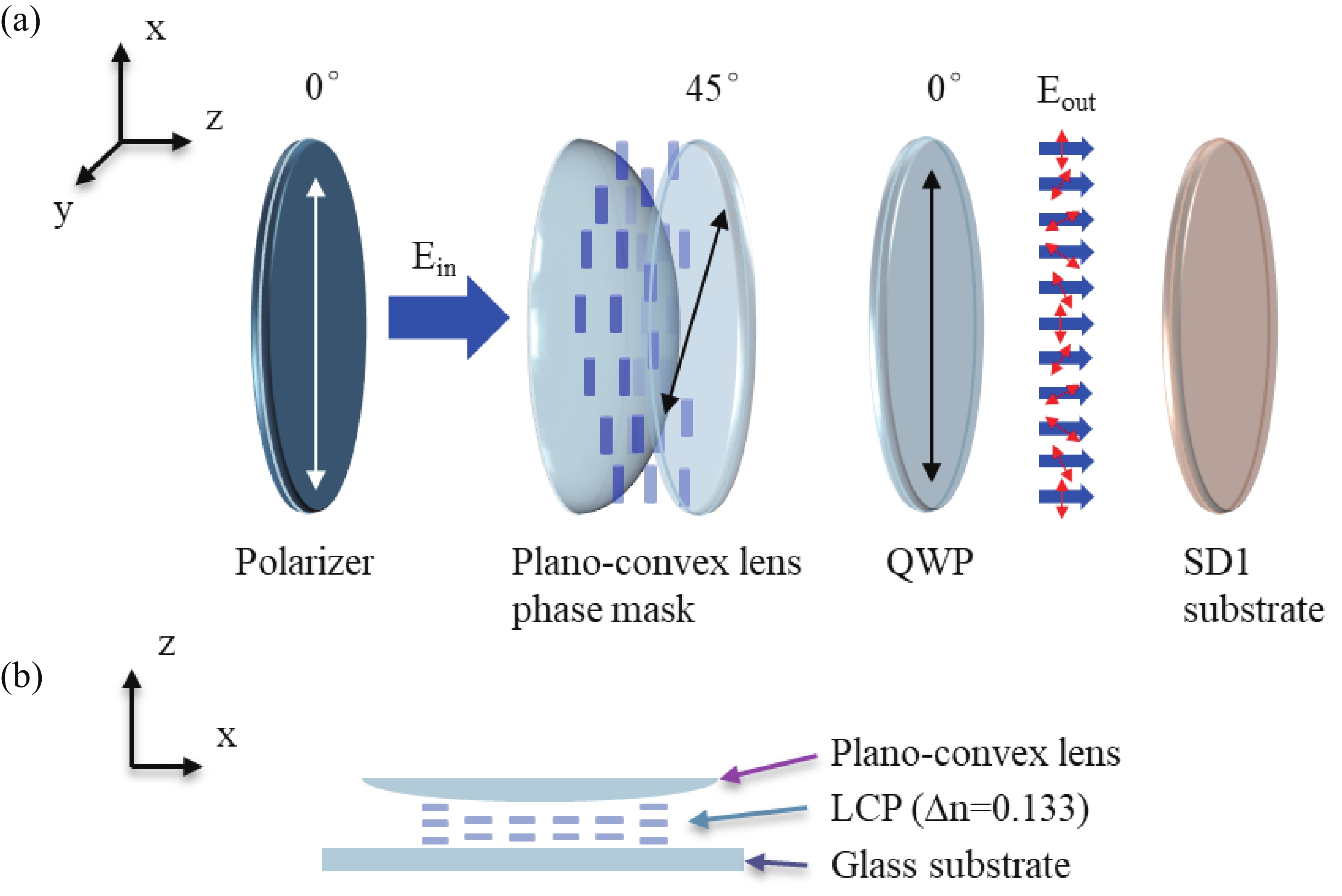
Abstract: The anisotropic absorption and emission from semiconductor CdSe/CdS quantum rods (QRs) provide extra benefits among other photoluminescence nanocrystals. Using photo-induced alignment technique, the QRs can be oriented in liquid crystal polymer matrix at a large scale. In this article, a 2D Dammann grating pattern, within “SKL” characters domains aligned QRs in composite film, was fabricated by multi-step photo exposure using several photo masks, and a continuous geometric lens profile pattern aligned QRs was realized by the single step polarization converting holographic irradiation method. Both polarized optical microscope and fluorescence microscope are employed to determine the liquid crystal director profiles and QRs anisotropic excitation properties. We have been able to orient the QRs in fine binary and continuous patterns that confirms the strong quantum rod aligning ability of the proposed method. Thus, the proposed approach paves a way for photo-induced flexible QRs alignments to provide a highly specific and difficult-to-replicate security application at a large scale.
Keywords: quantum rods, photo alignment, liquid crystal, flexible alignment, polarized emission
| [1] |
Haus J W, Zhou H S, Honma I, et al. Quantum confinement in semiconductor heterostructure nanometer-size particles. Phys Rev B, 1993, 47, 1359 doi: 10.1103/PhysRevB.47.1359
|
| [2] |
Huang H, Polavarapu L, Sichert J A, et al. Colloidal lead halide perovskite nanocrystals: Synthesis, optical properties and applications. NPG Asia Mater, 2016, 8, e328 doi: 10.1038/am.2016.167
|
| [3] |
Kim T H, Cho K S, Lee E K, et al. Full-colour quantum dot displays fabricated by transfer printing. Nature Photon, 2011, 5, 176 doi: 10.1038/nphoton.2011.12
|
| [4] |
Wang K, Sun X W. Quantum-dot and quantum-rod displays–the next big wave. Inf Disp, 2016, 32, 6 doi: 10.1002/j.2637-496X.2016.tb00948.x
|
| [5] |
Srivastava A K, Zhang W L, Schneider J, et al. Luminescent down-conversion semiconductor quantum dots and aligned quantum rods for liquid crystal displays. Adv Sci, 2019, 6, 1901345 doi: 10.1002/advs.201901345
|
| [6] |
Zhu R D, Luo Z Y, Chen H W, et al. Realizing Rec. 2020 color gamut with quantum dot displays. Opt Express, 2015, 23, 23680 doi: 10.1364/OE.23.023680
|
| [7] |
Luo Z Y, Chen Y, Wu S T. Wide color gamut LCD with a quantum dot backlight. Opt Express, 2013, 21, 26269 doi: 10.1364/OE.21.026269
|
| [8] |
Steckel J S, Ho J, Hamilton C, et al. Quantum dots: The ultimate down-conversion material for LCD displays. Jnl Soc Info Display, 2015, 23, 294 doi: 10.1002/jsid.313
|
| [9] |
Chen H W, He J, Wu S T. Recent advances on quantum-dot-enhanced liquid-crystal displays. IEEE J Sel Top Quantum Electron, 2017, 23, 1 doi: 10.1109/JSTQE.2017.2649466
|
| [10] |
Zhou Q C, Bai Z L, Lu W G, et al. In situ fabrication of halide perovskite nanocrystal-embedded polymer composite films with enhanced photoluminescence for display backlights. Adv Mater, 2016, 28, 9163 doi: 10.1002/adma.201602651
|
| [11] |
Yoon H C, Lee H, Kang H, et al. Highly efficient wide-color-gamut QD-emissive LCDs using red and green perovskite core/shell QDs. J Mater Chem C, 2018, 6, 13023 doi: 10.1039/C8TC04537B
|
| [12] |
Lu M, Zhang Y, Wang S X, et al. Metal halide perovskite light-emitting devices: Promising technology for next-generation displays. Adv Funct Materials, 2019, 29, 1902008 doi: 10.1002/adfm.201902008
|
| [13] |
Gao Y Y, Prodanov M F, Kang C B, et al. Stable bright perovskite nanoparticle thin porous films for color enhancement in modern liquid crystal displays. Nanoscale, 2021, 13, 6400 doi: 10.1039/D0NR07313J
|
| [14] |
Hu J T, Li L S, Yang W D, et al. Linearly polarized emission from colloidal semiconductor quantum rods. Science, 2001, 292, 2060 doi: 10.1126/science.1060810
|
| [15] |
Grivas C, Li C Y, Andreakou P, et al. Single-mode tunable laser emission in the single-exciton regime from colloidal nanocrystals. Nat Commun, 2013, 4, 2376 doi: 10.1038/ncomms3376
|
| [16] |
Diroll B T, Dadosh T, Koschitzky A, et al. Interpreting the energy-dependent anisotropy of colloidal nanorods using ensemble and single-particle spectroscopy. J Phys Chem C, 2013, 117, 23928 doi: 10.1021/jp407151f
|
| [17] |
Zhang X W, Xia J B. Linear-polarization optical property of CdSe quantum rods. Chin J Semicond, 2006, 27, 2094
|
| [18] |
Shabaev A, Efros A L. 1D exciton spectroscopy of semiconductor nanorods. Nano Lett, 2004, 4, 1821 doi: 10.1021/nl049216f
|
| [19] |
Seo D S, Kobayashi S, Nishikawa M. Study of the pretilt angle for 5CB on rubbed polyimide films containing trifluoromethyl moiety and analysis of the surface atomic concentration of F/C(%) with an electron spectroscope for chemical analysis. Appl Phys Lett, 1992, 61, 2392 doi: 10.1063/1.108174
|
| [20] |
Wang G W, Xiao J L. Frequency of the transition spectral line of an electron in quantum rods. J Semicond, 2010, 31, 092002 doi: 10.1088/1674-4926/31/9/092002
|
| [21] |
Xin W, Zhao Y W, Han C, et al. Magnetic field and temperature dependence of the properties of the ground state of the strong-coupling bound magnetopolaron in quantum rods with hydrogenic impurity. J Semicond, 2013, 34, 052001 doi: 10.1088/1674-4926/34/5/052001
|
| [22] |
Cunningham P D, Souza J B Jr, Fedin I, et al. Assessment of anisotropic semiconductor nanorod and nanoplatelet heterostructures with polarized emission for liquid crystal display technology. ACS Nano, 2016, 10, 5769 doi: 10.1021/acsnano.5b07949
|
| [23] |
Pisanello F, Leménager G, Martiradonna L, et al. Single-photon sources: Non-blinking single-photon generation with anisotropic colloidal nanocrystals: Towards room-temperature, efficient, colloidal quantum sources (adv. mater. 14/2013). Adv Mater, 2013, 25, 1973 doi: 10.1002/adma.201370091
|
| [24] |
Diroll B T, Koschitzky A, Murray C B. Tunable optical anisotropy of seeded CdSe/CdS nanorods. J Phys Chem Lett, 2014, 5, 85 doi: 10.1021/jz402426f
|
| [25] |
Baker J L, Widmer-Cooper A, Toney M F, et al. Device-scale perpendicular alignment of colloidal nanorods. Nano Lett, 2010, 10, 195 doi: 10.1021/nl903187v
|
| [26] |
Pietra F, Rabouw F T, van Rhee P G, et al. Self-assembled CdSe/CdS nanorod sheets studied in the bulk suspension by magnetic alignment. ACS Nano, 2014, 8, 10486 doi: 10.1021/nn503857t
|
| [27] |
Hu Z H, Fischbein M D, Querner C, et al. Electric-field-driven accumulation and alignment of CdSe and CdTe nanorods in nanoscale devices. Nano Lett, 2006, 6, 2585 doi: 10.1021/nl0620379
|
| [28] |
Mohammadimasoudi M, Penninck L, Aubert T, et al. Fast and versatile deposition of aligned semiconductor nanorods by dip-coating on a substrate with interdigitated electrodes. Opt Mater Express, 2013, 3, 2045 doi: 10.1364/OME.3.002045
|
| [29] |
Kaur S, Murali G, Manda R, et al. Functional film with electric-field-aided aligned assembly of quantum rods for potential application in liquid crystal display. Adv Opt Mater, 2018, 6, 1800235 doi: 10.1002/adom.201800235
|
| [30] |
Lutich A, Carbone L, Volchek S, et al. Macroscale alignment of CdSe/CdS nanorods by porous anodic alumina templates. Phys Stat Sol (RRL), 2009, 3, 151 doi: 10.1002/pssr.200903108
|
| [31] |
Amit Y, Faust A, Lieberman I, et al. Semiconductor nanorod layers aligned through mechanical rubbing. Phys Status Solidi A, 2012, 209, 235 doi: 10.1002/pssa.201127572
|
| [32] |
Li L S, Alivisatos A P. Semiconductor nanorod liquid crystals and their assembly on a substrate. Adv Mater, 2003, 15, 408 doi: 10.1002/adma.200390093
|
| [33] |
Kim F, Kwan S, Akana J, et al. Langmuir–blodgett nanorod assembly. J Am Chem Soc, 2001, 123, 4360 doi: 10.1021/ja0059138
|
| [34] |
Hasegawa M, Hirayama Y, Dertinger S. Polarized fluorescent emission from aligned electrospun nanofiber sheets containing semiconductor nanorods. Appl Phys Lett, 2015, 106, 051103 doi: 10.1063/1.4907548
|
| [35] |
Du T, Schneider J, Srivastava A K, et al. Combination of photoinduced alignment and self-assembly to realize polarized emission from ordered semiconductor nanorods. ACS Nano, 2015, 9, 11049 doi: 10.1021/acsnano.5b04483
|
| [36] |
Schneider J, Zhang W L, Srivastava A K, et al. Photoinduced micropattern alignment of semiconductor nanorods with polarized emission in a liquid crystal polymer matrix. Nano Lett, 2017, 17, 3133 doi: 10.1021/acs.nanolett.7b00563
|
| [37] |
Srivastava A K, Zhang W L, Schneider J, et al. Photoaligned nanorod enhancement films with polarized emission for liquid-crystal-display applications. Adv Mater, 2017, 29, 1701091 doi: 10.1002/adma.201701091
|
| [38] |
Zhang W L, Schneider J, Chigrinov V G, et al. Optically addressable photoaligned semiconductor nanorods in thin liquid crystal films for display applications. Adv Opt Mater, 2018, 6, 1800250 doi: 10.1002/adom.201800250
|
| [39] |
Dudka T, Zhang W L, Schneider J, et al. Formulation of a composite system of liquid crystals and light-emitting semiconductor quantum rods: From assemblies in solution to photoaligned films. Adv Mater Technol, 2019, 4, 1900695 doi: 10.1002/admt.201900695
|
| [40] |
Gupta S K, Prodanov M F, Zhang W L, et al. Inkjet-printed aligned quantum rod enhancement films for their application in liquid crystal displays. Nanoscale, 2019, 11, 20837 doi: 10.1039/C9NR06881C
|
| [41] |
Kang C B, Zhou Z C, Halpert J E, et al. Inkjet printed patterned bank structure with encapsulated perovskite colour filters for modern display. Nanoscale, 2022, 14, 8060 doi: 10.1039/D2NR00849A
|
| [42] |
Zhang W L, Prodanov M F, Schneider J, et al. Ligand shell engineering to achieve optimal photoalignment of semiconductor quantum rods for liquid crystal displays. Adv Funct Mater, 2019, 29, 1805094 doi: 10.1002/adfm.201805094
|
| [43] |
Prodanov M F, Kang C B, Gupta S K, et al. Unidirectionally aligned bright quantum rods films, using T-shape ligands, for LCD application. Nano Res, 2022, 15, 5392 doi: 10.1007/s12274-021-4019-2
|
| [44] |
Prodanov M F, Gupta S K, Kang C B, et al. Thermally stable quantum rods, covering full visible range for display and lighting application. Small, 2021, 17, e2004487 doi: 10.1002/smll.202004487
|
| [45] |
Kang C B, Prodanov M F, Gao Y Y, et al. Quantum-rod on-chip LEDs for display backlights with efficacy of 149lmW–1: A step toward 200lmW–1. Adv Mater, 2021, 33, 2104685 doi: 10.1002/adma.202104685
|
| [46] |
Srivastava A K, Hu W, Chigrinov V G, et al. Fast switchable grating based on orthogonal photo alignments of ferroelectric liquid crystals. Appl Phys Lett, 2012, 101, 031112 doi: 10.1063/1.4737642
|
| [47] |
Chigrinov V, Pikin S, Verevochnikov A, et al. Diffusion model of photoaligning in azo-dye layers. Phys Rev E, 2004, 69, 061713 doi: 10.1103/PhysRevE.69.061713
|
| [48] |
Shteyner E A, Srivastava A K, Chigrinov V G, et al. Submicron-scale liquid crystal photo-alignment. Soft Matter, 2013, 9, 5160 doi: 10.1039/c3sm50498k
|
| [49] |
Dammann H, Görtler K. High-efficiency in-line multiple imaging by means of multiple phase holograms. Opt Commun, 1971, 3, 312 doi: 10.1016/0030-4018(71)90095-2
|
| [50] |
Tam A M , Fan F, Du T, et al. Bifocal optical-vortex lens with sorting of the generated nonseparable spin-orbital angular-momentum states. Phys Rev Applied, 2017, 7, 034010 doi: 10.1103/PhysRevApplied.7.034010
|


Article views: 1866 Times PDF downloads: 104 Times Cited by: 0 Times
Received: 14 August 2023 Revised: 13 September 2023 Online: Accepted Manuscript: 15 September 2023Corrected proof: 15 September 2023Published: 10 September 2023
| Citation: |
Wanlong Zhang, Julian Schneider, Maksym F. Prodanov, Valerii V. Vashchenko, Andrey L. Rogach, Xiaocong Yuan, Abhishek K. Srivastava. Photo-induced flexible semiconductor CdSe/CdS quantum rods alignment[J]. Journal of Semiconductors, 2023, 44(9): 092605. doi: 10.1088/1674-4926/44/9/092605
****
W L Zhang, J Schneider, M F Prodanov, V V Vashchenko, A L Rogach, X C Yuan, A K Srivastava. Photo-induced flexible semiconductor CdSe/CdS quantum rods alignment[J]. J. Semicond, 2023, 44(9): 092605. doi: 10.1088/1674-4926/44/9/092605

|
 Wanlong Zhang:received his Ph.D. degree in 2019 from the Hong Kong University of Science and Technology. Now he is an assistant professor in Shenzhen University. His research interests include liquid crystal photoalignment, liquid crystal photonics, liquid crystal on silicon, optical neural network and optical field manipulation
 Abhishek K. Srivastava:is an Associate Professor and Associate Director of Centre for Display Research, at the Hong Kong University of Science and Technology. He received his Ph.D. degree in 2009 from the University of Lucknow, India. He is the Editor-in-Chief of Journal of the Society for Information Displays. He is a senior member of the Society for Information Display (SID), United States, and a member of IEEE. His current research interests include photo-alignment technology, nanomaterials, and fast liquid crystals for advanced displays and photonic devices. In 2014, he received the ILCS Early-Career Award: The Michi Nakata Prize for his early career efforts in the field of ferroelectric liquid crystals and photo-alignment. In 2018, he received the best I-zone display prototype of the year award from the SID display week for the ferroelectric liquid crystal displays. In the same year, he received the LG Bronze award from the Korean information display society for the newly developed quantum rod enhancement film. To date, he has published 228 research papers and holds 44 patents/patent applications
| [1] |
Haus J W, Zhou H S, Honma I, et al. Quantum confinement in semiconductor heterostructure nanometer-size particles. Phys Rev B, 1993, 47, 1359 doi: 10.1103/PhysRevB.47.1359
|
| [2] |
Huang H, Polavarapu L, Sichert J A, et al. Colloidal lead halide perovskite nanocrystals: Synthesis, optical properties and applications. NPG Asia Mater, 2016, 8, e328 doi: 10.1038/am.2016.167
|
| [3] |
Kim T H, Cho K S, Lee E K, et al. Full-colour quantum dot displays fabricated by transfer printing. Nature Photon, 2011, 5, 176 doi: 10.1038/nphoton.2011.12
|
| [4] |
Wang K, Sun X W. Quantum-dot and quantum-rod displays–the next big wave. Inf Disp, 2016, 32, 6 doi: 10.1002/j.2637-496X.2016.tb00948.x
|
| [5] |
Srivastava A K, Zhang W L, Schneider J, et al. Luminescent down-conversion semiconductor quantum dots and aligned quantum rods for liquid crystal displays. Adv Sci, 2019, 6, 1901345 doi: 10.1002/advs.201901345
|
| [6] |
Zhu R D, Luo Z Y, Chen H W, et al. Realizing Rec. 2020 color gamut with quantum dot displays. Opt Express, 2015, 23, 23680 doi: 10.1364/OE.23.023680
|
| [7] |
Luo Z Y, Chen Y, Wu S T. Wide color gamut LCD with a quantum dot backlight. Opt Express, 2013, 21, 26269 doi: 10.1364/OE.21.026269
|
| [8] |
Steckel J S, Ho J, Hamilton C, et al. Quantum dots: The ultimate down-conversion material for LCD displays. Jnl Soc Info Display, 2015, 23, 294 doi: 10.1002/jsid.313
|
| [9] |
Chen H W, He J, Wu S T. Recent advances on quantum-dot-enhanced liquid-crystal displays. IEEE J Sel Top Quantum Electron, 2017, 23, 1 doi: 10.1109/JSTQE.2017.2649466
|
| [10] |
Zhou Q C, Bai Z L, Lu W G, et al. In situ fabrication of halide perovskite nanocrystal-embedded polymer composite films with enhanced photoluminescence for display backlights. Adv Mater, 2016, 28, 9163 doi: 10.1002/adma.201602651
|
| [11] |
Yoon H C, Lee H, Kang H, et al. Highly efficient wide-color-gamut QD-emissive LCDs using red and green perovskite core/shell QDs. J Mater Chem C, 2018, 6, 13023 doi: 10.1039/C8TC04537B
|
| [12] |
Lu M, Zhang Y, Wang S X, et al. Metal halide perovskite light-emitting devices: Promising technology for next-generation displays. Adv Funct Materials, 2019, 29, 1902008 doi: 10.1002/adfm.201902008
|
| [13] |
Gao Y Y, Prodanov M F, Kang C B, et al. Stable bright perovskite nanoparticle thin porous films for color enhancement in modern liquid crystal displays. Nanoscale, 2021, 13, 6400 doi: 10.1039/D0NR07313J
|
| [14] |
Hu J T, Li L S, Yang W D, et al. Linearly polarized emission from colloidal semiconductor quantum rods. Science, 2001, 292, 2060 doi: 10.1126/science.1060810
|
| [15] |
Grivas C, Li C Y, Andreakou P, et al. Single-mode tunable laser emission in the single-exciton regime from colloidal nanocrystals. Nat Commun, 2013, 4, 2376 doi: 10.1038/ncomms3376
|
| [16] |
Diroll B T, Dadosh T, Koschitzky A, et al. Interpreting the energy-dependent anisotropy of colloidal nanorods using ensemble and single-particle spectroscopy. J Phys Chem C, 2013, 117, 23928 doi: 10.1021/jp407151f
|
| [17] |
Zhang X W, Xia J B. Linear-polarization optical property of CdSe quantum rods. Chin J Semicond, 2006, 27, 2094
|
| [18] |
Shabaev A, Efros A L. 1D exciton spectroscopy of semiconductor nanorods. Nano Lett, 2004, 4, 1821 doi: 10.1021/nl049216f
|
| [19] |
Seo D S, Kobayashi S, Nishikawa M. Study of the pretilt angle for 5CB on rubbed polyimide films containing trifluoromethyl moiety and analysis of the surface atomic concentration of F/C(%) with an electron spectroscope for chemical analysis. Appl Phys Lett, 1992, 61, 2392 doi: 10.1063/1.108174
|
| [20] |
Wang G W, Xiao J L. Frequency of the transition spectral line of an electron in quantum rods. J Semicond, 2010, 31, 092002 doi: 10.1088/1674-4926/31/9/092002
|
| [21] |
Xin W, Zhao Y W, Han C, et al. Magnetic field and temperature dependence of the properties of the ground state of the strong-coupling bound magnetopolaron in quantum rods with hydrogenic impurity. J Semicond, 2013, 34, 052001 doi: 10.1088/1674-4926/34/5/052001
|
| [22] |
Cunningham P D, Souza J B Jr, Fedin I, et al. Assessment of anisotropic semiconductor nanorod and nanoplatelet heterostructures with polarized emission for liquid crystal display technology. ACS Nano, 2016, 10, 5769 doi: 10.1021/acsnano.5b07949
|
| [23] |
Pisanello F, Leménager G, Martiradonna L, et al. Single-photon sources: Non-blinking single-photon generation with anisotropic colloidal nanocrystals: Towards room-temperature, efficient, colloidal quantum sources (adv. mater. 14/2013). Adv Mater, 2013, 25, 1973 doi: 10.1002/adma.201370091
|
| [24] |
Diroll B T, Koschitzky A, Murray C B. Tunable optical anisotropy of seeded CdSe/CdS nanorods. J Phys Chem Lett, 2014, 5, 85 doi: 10.1021/jz402426f
|
| [25] |
Baker J L, Widmer-Cooper A, Toney M F, et al. Device-scale perpendicular alignment of colloidal nanorods. Nano Lett, 2010, 10, 195 doi: 10.1021/nl903187v
|
| [26] |
Pietra F, Rabouw F T, van Rhee P G, et al. Self-assembled CdSe/CdS nanorod sheets studied in the bulk suspension by magnetic alignment. ACS Nano, 2014, 8, 10486 doi: 10.1021/nn503857t
|
| [27] |
Hu Z H, Fischbein M D, Querner C, et al. Electric-field-driven accumulation and alignment of CdSe and CdTe nanorods in nanoscale devices. Nano Lett, 2006, 6, 2585 doi: 10.1021/nl0620379
|
| [28] |
Mohammadimasoudi M, Penninck L, Aubert T, et al. Fast and versatile deposition of aligned semiconductor nanorods by dip-coating on a substrate with interdigitated electrodes. Opt Mater Express, 2013, 3, 2045 doi: 10.1364/OME.3.002045
|
| [29] |
Kaur S, Murali G, Manda R, et al. Functional film with electric-field-aided aligned assembly of quantum rods for potential application in liquid crystal display. Adv Opt Mater, 2018, 6, 1800235 doi: 10.1002/adom.201800235
|
| [30] |
Lutich A, Carbone L, Volchek S, et al. Macroscale alignment of CdSe/CdS nanorods by porous anodic alumina templates. Phys Stat Sol (RRL), 2009, 3, 151 doi: 10.1002/pssr.200903108
|
| [31] |
Amit Y, Faust A, Lieberman I, et al. Semiconductor nanorod layers aligned through mechanical rubbing. Phys Status Solidi A, 2012, 209, 235 doi: 10.1002/pssa.201127572
|
| [32] |
Li L S, Alivisatos A P. Semiconductor nanorod liquid crystals and their assembly on a substrate. Adv Mater, 2003, 15, 408 doi: 10.1002/adma.200390093
|
| [33] |
Kim F, Kwan S, Akana J, et al. Langmuir–blodgett nanorod assembly. J Am Chem Soc, 2001, 123, 4360 doi: 10.1021/ja0059138
|
| [34] |
Hasegawa M, Hirayama Y, Dertinger S. Polarized fluorescent emission from aligned electrospun nanofiber sheets containing semiconductor nanorods. Appl Phys Lett, 2015, 106, 051103 doi: 10.1063/1.4907548
|
| [35] |
Du T, Schneider J, Srivastava A K, et al. Combination of photoinduced alignment and self-assembly to realize polarized emission from ordered semiconductor nanorods. ACS Nano, 2015, 9, 11049 doi: 10.1021/acsnano.5b04483
|
| [36] |
Schneider J, Zhang W L, Srivastava A K, et al. Photoinduced micropattern alignment of semiconductor nanorods with polarized emission in a liquid crystal polymer matrix. Nano Lett, 2017, 17, 3133 doi: 10.1021/acs.nanolett.7b00563
|
| [37] |
Srivastava A K, Zhang W L, Schneider J, et al. Photoaligned nanorod enhancement films with polarized emission for liquid-crystal-display applications. Adv Mater, 2017, 29, 1701091 doi: 10.1002/adma.201701091
|
| [38] |
Zhang W L, Schneider J, Chigrinov V G, et al. Optically addressable photoaligned semiconductor nanorods in thin liquid crystal films for display applications. Adv Opt Mater, 2018, 6, 1800250 doi: 10.1002/adom.201800250
|
| [39] |
Dudka T, Zhang W L, Schneider J, et al. Formulation of a composite system of liquid crystals and light-emitting semiconductor quantum rods: From assemblies in solution to photoaligned films. Adv Mater Technol, 2019, 4, 1900695 doi: 10.1002/admt.201900695
|
| [40] |
Gupta S K, Prodanov M F, Zhang W L, et al. Inkjet-printed aligned quantum rod enhancement films for their application in liquid crystal displays. Nanoscale, 2019, 11, 20837 doi: 10.1039/C9NR06881C
|
| [41] |
Kang C B, Zhou Z C, Halpert J E, et al. Inkjet printed patterned bank structure with encapsulated perovskite colour filters for modern display. Nanoscale, 2022, 14, 8060 doi: 10.1039/D2NR00849A
|
| [42] |
Zhang W L, Prodanov M F, Schneider J, et al. Ligand shell engineering to achieve optimal photoalignment of semiconductor quantum rods for liquid crystal displays. Adv Funct Mater, 2019, 29, 1805094 doi: 10.1002/adfm.201805094
|
| [43] |
Prodanov M F, Kang C B, Gupta S K, et al. Unidirectionally aligned bright quantum rods films, using T-shape ligands, for LCD application. Nano Res, 2022, 15, 5392 doi: 10.1007/s12274-021-4019-2
|
| [44] |
Prodanov M F, Gupta S K, Kang C B, et al. Thermally stable quantum rods, covering full visible range for display and lighting application. Small, 2021, 17, e2004487 doi: 10.1002/smll.202004487
|
| [45] |
Kang C B, Prodanov M F, Gao Y Y, et al. Quantum-rod on-chip LEDs for display backlights with efficacy of 149lmW–1: A step toward 200lmW–1. Adv Mater, 2021, 33, 2104685 doi: 10.1002/adma.202104685
|
| [46] |
Srivastava A K, Hu W, Chigrinov V G, et al. Fast switchable grating based on orthogonal photo alignments of ferroelectric liquid crystals. Appl Phys Lett, 2012, 101, 031112 doi: 10.1063/1.4737642
|
| [47] |
Chigrinov V, Pikin S, Verevochnikov A, et al. Diffusion model of photoaligning in azo-dye layers. Phys Rev E, 2004, 69, 061713 doi: 10.1103/PhysRevE.69.061713
|
| [48] |
Shteyner E A, Srivastava A K, Chigrinov V G, et al. Submicron-scale liquid crystal photo-alignment. Soft Matter, 2013, 9, 5160 doi: 10.1039/c3sm50498k
|
| [49] |
Dammann H, Görtler K. High-efficiency in-line multiple imaging by means of multiple phase holograms. Opt Commun, 1971, 3, 312 doi: 10.1016/0030-4018(71)90095-2
|
| [50] |
Tam A M , Fan F, Du T, et al. Bifocal optical-vortex lens with sorting of the generated nonseparable spin-orbital angular-momentum states. Phys Rev Applied, 2017, 7, 034010 doi: 10.1103/PhysRevApplied.7.034010
|

 WeChat ID
Journal of Semiconductors © 2017 All Rights Reserved 京ICP备05085259号-2

 DownLoad:

