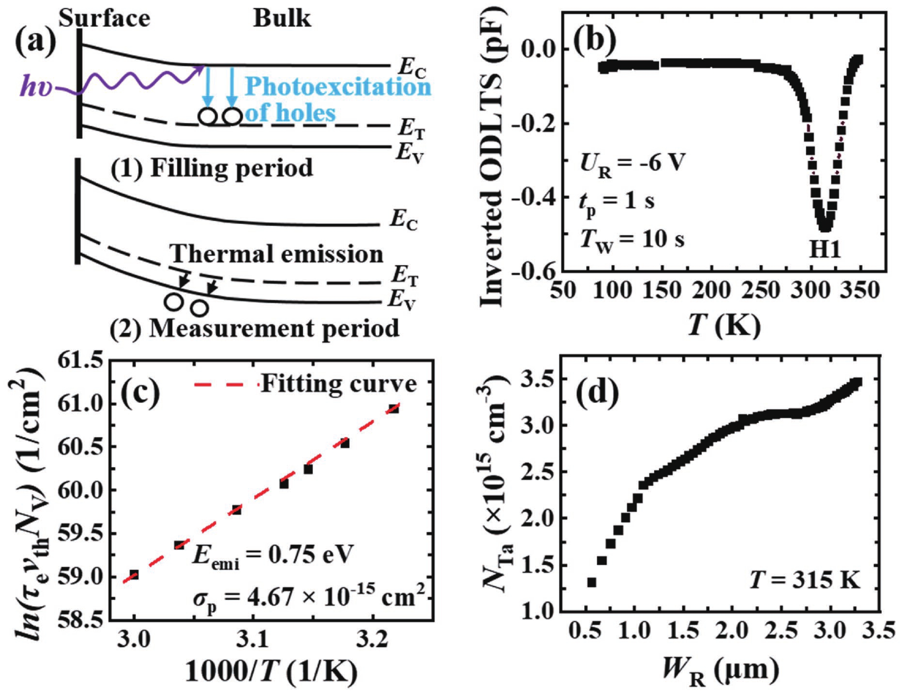
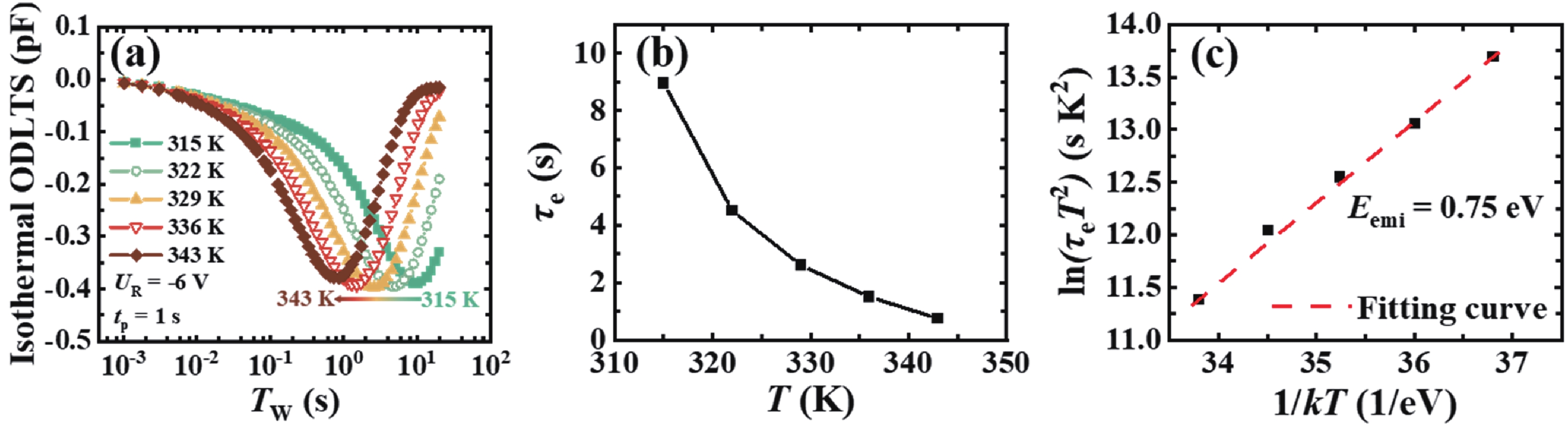
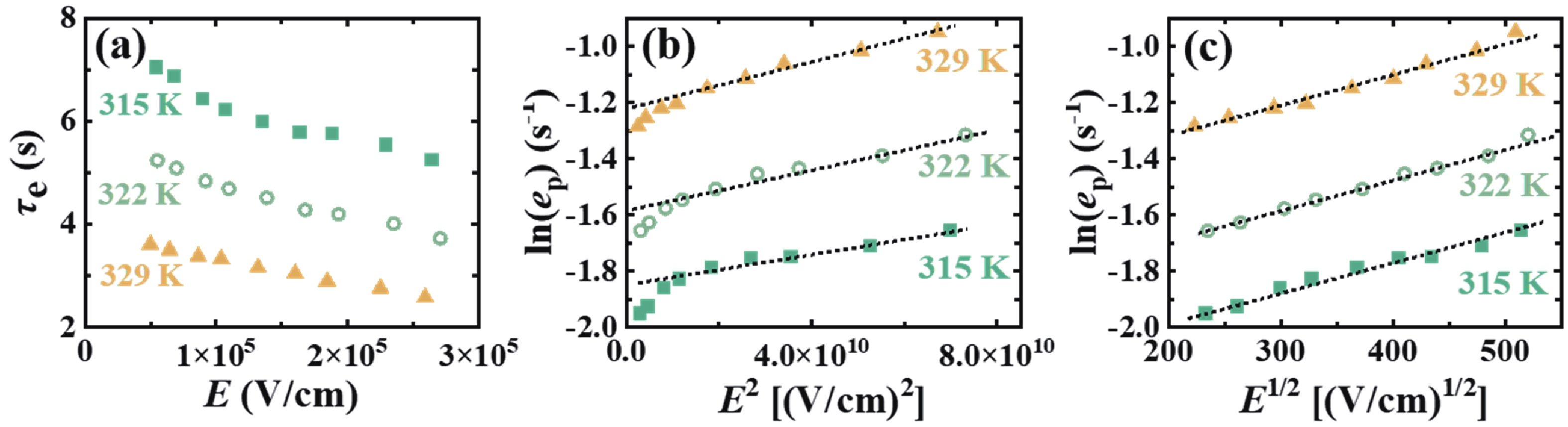
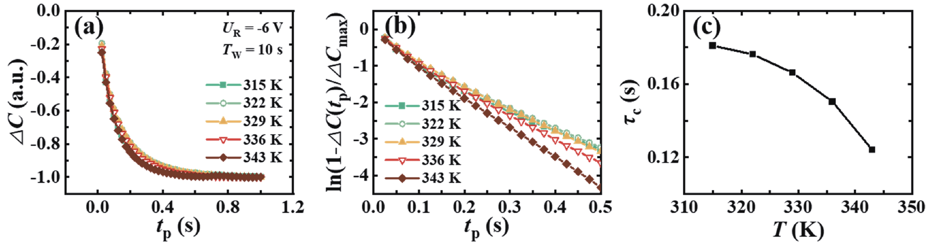
| [1] |
Flack T J, Pushpakaran B N, Bayne S B. GaN technology for power electronic applications: A review. J Electron Mater, 2016, 45, 2673 doi: 10.1007/s11664-016-4435-3 |
| [2] |
Li G Q, Wang W L, Yang W J, et al. GaN-based light-emitting diodes on various substrates: A critical review. Rep Prog Phys, 2016, 79, 056501 doi: 10.1088/0034-4885/79/5/056501 |
| [3] |
Kunwar S, Pandit S, Jeong J H, et al. Improved photoresponse of UV photodetectors by the incorporation of plasmonic nanoparticles on GaN through the resonant coupling of localized surface plasmon resonance. Nanomicro Lett, 2020, 12, 91 doi: 10.1007/s40820-020-00437-x |
| [4] |
Jiang C Y, Jing L, Huang X, et al. Enhanced solar cell conversion efficiency of InGaN/GaN multiple quantum wells by piezo-phototronic effect. ACS Nano, 2017, 11, 9405 doi: 10.1021/acsnano.7b04935 |
| [5] |
Lei P, Li C Z, Wang D D, et al. Carbon-induced deep traps responsible for current collapse in AlGaN/GaN HEMTs. J Semicond, 2008, 29, 1066
|
| [6] |
Zhang Y M, Feng S W, Zhu H, et al. Self-heating and traps effects on the drain transient response of AlGaN/GaN HEMTs. J Semicond, 2014, 35, 104003 doi: 10.1088/1674-4926/35/10/104003 |
| [7] |
Zhou X Y, Tan X, Wang Y G, et al. Coeffect of trapping behaviors on the performance of GaN-based devices. J Semicond, 2018, 39, 094007 doi: 10.1088/1674-4926/39/9/094007 |
| [8] |
Hezabra A, Abdeslam N A, Sengouga N, et al. 2D study of AlGaN/AlN/GaN/AlGaN HEMTs’ response to traps. J Semicond, 2019, 40, 022802 doi: 10.1088/1674-4926/40/2/022802 |
| [9] |
Angelotti A M, Gibiino G P, Santarelli A, et al. Experimental characterization of charge trapping dynamics in 100-nm AlN/GaN/AlGaN-on-Si HEMTs by wideband transient measurements. IEEE Trans Electron Devices, 2020, 67, 3069 doi: 10.1109/TED.2020.3000983 |
| [10] |
|
| [11] |
Chen J X, Zhu M, Lu X, et al. Electrical characterization of GaN Schottky barrier diode at cryogenic temperatures. Appl Phys Lett, 2020, 116, 062102 doi: 10.1063/1.5131337 |
| [12] |
Zhang Y L, Zhang X, Zhu M, et al. Forward conduction instability of quasi-vertical GaN p-i-n diodes on Si substrates. IEEE Trans Electron Devices, 2020, 67, 3992 doi: 10.1109/TED.2020.3012422 |
| [13] |
Tokuda Y, Matsuoka Y, Ueda H, et al. DLTS study of n-type GaN grown by MOCVD on GaN substrates. Superlattices Microstruct, 2006, 40, 268 doi: 10.1016/j.spmi.2006.07.025 |
| [14] |
Kogiso T, Narita T, Yoshida H, et al. Characterization of hole traps in MOVPE-grown p-type GaN layers using low-frequency capacitance deep-level transient spectroscopy. Jpn J Appl Phys, 2019, 58, SCCB36 doi: 10.7567/1347-4065/ab0408 |
| [15] |
Kanegae K, Fujikura H, Otoki Y, et al. Deep-level transient spectroscopy studies of electron and hole traps in n-type GaN homoepitaxial layers grown by quartz-free hydride-vapor-phase epitaxy. Appl Phys Lett, 2019, 115, 012103 doi: 10.1063/1.5098965 |
| [16] |
Arehart A R, Corrion A, Poblenz C, et al. Comparison of deep level incorporation in ammonia and rf-plasma assisted molecular beam epitaxy n-GaN films. Phys Status Solidi (c), 2008, 5, 1750 doi: 10.1002/pssc.200778622 |
| [17] |
Zhu M, Ren Y, Zhou L D, et al. Temperature-dependent electrical characteristics of neutron-irradiated GaN Schottky barrier diodes. Microelectron Reliab, 2021, 125, 114345 doi: 10.1016/j.microrel.2021.114345 |
| [18] |
Alfieri G, Sundaramoorthy V K. Minority carrier traps in ion-implanted n-type homoepitaxial GaN. Phys Status Solidi B Basic Res, 2020, 257, 1900506 doi: 10.1002/pssb.201900506 |
| [19] |
Polyakov A Y, Smirnov N B, Govorkov A V, et al. Deep hole traps in n-GaN films grown by hydride vapor phase epitaxy. J Appl Phys, 2002, 91, 6580 doi: 10.1063/1.1468909 |
| [20] |
Amor S, Ahaitouf A, Ahaitouf A, et al. Evidence of minority carrier traps contribution in deep level transient spectroscopy measurement in n–GaN Schottky diode. Superlattices Microstruct, 2017, 101, 529 doi: 10.1016/j.spmi.2016.11.011 |
| [21] |
Duc T T, Pozina G, Amano H, et al. Deep level study of Mg-doped GaN using deep level transient spectroscopy and minority carrier transient spectroscopy. Phys Rev B, 2016, 94, 045206 doi: 10.1103/PhysRevB.94.045206 |
| [22] |
Kanegae K, Horita M, Kimoto T, et al. Accurate method for estimating hole trap concentration in n-type GaN via minority carrier transient spectroscopy. Appl Phys Express, 2018, 11, 071002 doi: 10.7567/APEX.11.071002 |
| [23] |
Polyakov A Y, Smirnov N B, Govorkov A V, et al. Hydride vapor phase GaN films with reduced density of residual electrons and deep traps. J Appl Phys, 2014, 115, 183706 doi: 10.1063/1.4876061 |
| [24] |
Polyakov A Y, Smirnov N B, Yakimov E B, et al. Electrical, optical, and structural properties of GaN films prepared by hydride vapor phase epitaxy. J Alloys Compd, 2014, 617, 200 doi: 10.1016/j.jallcom.2014.07.208 |
| [25] |
Polyakov A Y, Lee I H, Smirnov N B, et al. Electric field dependence of major electron trap emission in bulk β-Ga 2O 3: Poole–Frenkel effect versus phonon-assisted tunneling. J Phys D:Appl Phys, 2020, 53, 304001 doi: 10.1088/1361-6463/ab87c1 |
| [26] |
Qu H L, Zou X B. Emission and capture characteristics of electron trap (E emi = 0.8 eV) in Si-doped β-Ga 2O 3 epilayer. Semicond Sci Technol, 2023, 38, 015001 doi: 10.1088/1361-6641/aca045 |
| [27] |
Markevich V P, Halsall M P, Sun L J, et al. Electric-field enhancement of electron emission rates for deep-level traps in n-type GaN. Phys Status Solidi B Basic Res, 2023, 260, 2200545 doi: 10.1002/pssb.202200545 |
| [28] |
Cho H K, Kim C S, Hong C H. Electron capture behaviors of deep level traps in unintentionally doped and intentionally doped n-type GaN. J Appl Phys, 2003, 94, 1485 doi: 10.1063/1.1586981 |
| [29] |
Wang Z P, Chen X H, Ren F F, et al. Deep-level defects in gallium oxide. J Phys D:Appl Phys, 2021, 54, 043002 doi: 10.1088/1361-6463/abbeb1 |
| [30] |
Peaker A R, Markevich V P, Coutinho J. Tutorial: Junction spectroscopy techniques and deep-level defects in semiconductors. J Appl Phys, 2018, 123, 161559 doi: 10.1063/1.5011327 |
| [31] |
Kanegae K, Narita T, Tomita K, et al. Dual-color-sub-bandgap-light-excited isothermal capacitance transient spectroscopy for quick measurement of carbon-related hole trap density in n-type GaN. Jpn J Appl Phys, 2020, 59, SGGD05 doi: 10.35848/1347-4065/ab6863 |
| [32] |
Lang D V. Fast capacitance transient appartus: Application to ZnO and O centers in GaP p−n junctions. J Appl Phys, 1974, 45, 3014 doi: 10.1063/1.1663718 |
| [33] |
Martin G M, Mitonneau A, Pons D, et al. Detailed electrical characterisation of the deep Cr acceptor in GaAs. J Phys C Solid State Phys, 1980, 13, 3855 doi: 10.1088/0022-3719/13/20/009 |
| [34] |
Tian Z, Quick N R, Kar A. Characteristics of 6H-silicon carbide PIN diodes prototyping by laser doping. J Electron Mater, 2005, 34, 430 doi: 10.1007/s11664-005-0123-4 |
| [35] |
Chen J X, Luo H X, Qu H L, et al. Single-trap emission kinetics of vertical β-Ga 2O 3 Schottky diodes by deep-level transient spectroscopy. Semicond Sci Technol, 2021, 36, 055015 doi: 10.1088/1361-6641/abed8d |
| [36] |
Aoshima K, Kanegae K, Horita M, et al. Electron traps formed by gamma-ray irradiation in homoepitaxial n-type GaN and their annealing behavior. AIP Adv, 2020, 10, 045023 doi: 10.1063/1.5144158 |
| [37] |
Chen J X, Huang W, Qu H L, et al. Study of minority carrier traps in p-GaN gate HEMT by optical deep level transient spectroscopy. Appl Phys Lett, 2022, 120, 212105 doi: 10.1063/5.0083362 |
| [38] |
Coelho A V P, Boudinov H. Emission rate dependence on the electric field for two trap levels in proton-irradiated n-type GaAs. Phys Rev B, 2008, 77, 235210 doi: 10.1103/PhysRevB.77.235210 |
| [39] |
Kumar A, Mondal S, Rao K S R K. DLTS analysis of amphoteric interface defects in high-TiO 2 MOS structures prepared by sol-gel spin-coating. AIP Adv, 2015, 5, 117122 doi: 10.1063/1.4935749 |
| [40] |
Heo S, Chung J, Lee H I, et al. Defect visualization of Cu(InGa)(SeS) 2 thin films using DLTS measurement. Sci Rep, 2016, 6, 30554 doi: 10.1038/srep30554 |
| [41] |
Pons D. Accurate determination of the free carrier capture kinetics of deep traps by space-charge methods. J Appl Phys, 1984, 55, 3644 doi: 10.1063/1.332914 |
| [42] |
Tokuda Y, Yamada Y, Shibata T, et al. Hole traps in n-GaN detected by minority carrier transient spectroscopy. Phys Status Solidi C, 2011, 8, 2239 doi: 10.1002/pssc.201000879 |
| [43] |
Hamilton B, Peaker A R, Wight D R. Deep-state-controlled minority-carrier lifetime in n-type gallium phosphide. J Appl Phys, 1979, 50, 6373 doi: 10.1063/1.325728 |
| [44] |
Shah P B, Dedhia R H, Tompkins R P, et al. DLTS and MCTS analysis of the influence of growth pressure on trap generation in MOCVD GaN. Solid State Electron, 2012, 78, 121 doi: 10.1016/j.sse.2012.05.057 |


 Jin Sui got her BS from Xidian University in 2019. Now she is a master’s student at ShanghaiTech Univeristy under the supervision of Prof. Xinbo Zou. Her research focuses on device transient characteristics and low frequency noise characteristics of GaN power diodes.
 Xinbo Zou received his B.Eng degree from Beijing University of Posts and Telecommunications (BUPT) in 2007 and Ph.D from the Hong Kong University of Science and Technology (HKUST) in 2013. From 2014 to 2017, he was a Research Assistant Professor with the Department of Electronic and Computer Engineering and a Junior Fellow at the Institute for Advanced Study (IAS) of HKUST. In September 2017, he joined ShanghaiTech University as an assistant professor. His research focuses on characterization of Ⅲ-N materials and devices, encompassing thin-film and nano-scale devices.
 DownLoad: