J. Semicond. > 2024, Volume 45 > Issue 4 > 042301

ARTICLES

On the relationship between imprint and reliability in Hf0.5Zr0.5O2 based ferroelectric random access memory

Peng Yuan, Yuting Chen, Liguo Chai, Zhengying Jiao, Qingjie Luan, Yongqing Shen, Ying Zhang, Jibin Leng, Xueli Ma, Jinjuan Xiang, Guilei Wang and Chao Zhao

+ Author Affiliations

 Corresponding author: Xueli Ma, Xueli.ma@bjsamt.org.cn; Jinjuan Xiang, Jinjuan.Xiang@bjsamt.org.cn; Guilei Wang, Guilei.Wang@bjsamt.org.cn

DOI: 10.1088/1674-4926/45/4/042301

PDF

Turn off MathJax

Abstract: The detrimental effect of imprint, which can cause misreading problem, has hindered the application of ferroelectric HfO2. In this work, we present results of a comprehensive reliability evaluation of Hf0.5Zr0.5O2-based ferroelectric random access memory. The influence of imprint on the retention and endurance is demonstrated. Furthermore, a solution in circuity is proposed to effectively solve the misreading problem caused by imprint.

Key words: FeRAMHZOimprintreliability

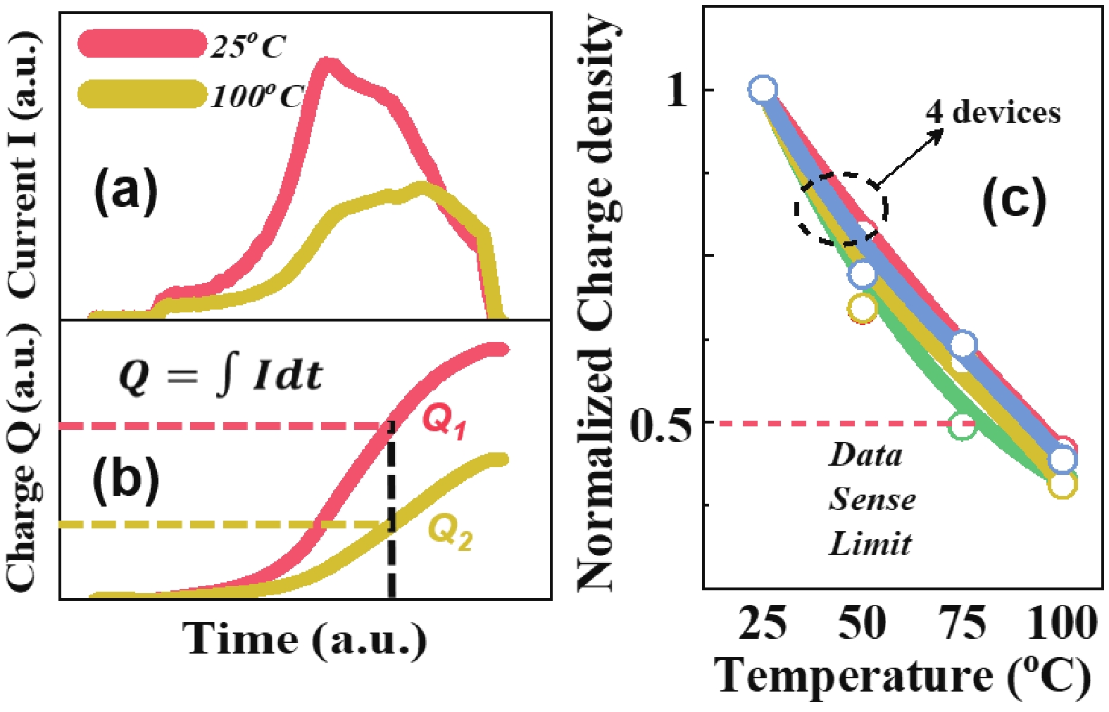
Ferroelectric memory (FRAM) offers unique capabilities which make it an attractive non-volatile memory choice for many applications[13]. Since Böscke et al. discovered the ferroelectricity in nanoscale HfO2 in 2011 for the first time[4], the scaling down problem that plagues traditional ferroelectricity has been greatly promoted. Meanwhile, ferroelectric HfO2 (FE-HfO2) starts a new future for memory generations due to its distinctive features include RAM-like, write speeds, low voltage, low power write operation, high cycling endurance lifetime and architectural flexibility[57]. However, certain reliability issues must be satisfactorily resolved before they can be widely applied in commercial memories. Imprint problem, as one of the reliability issues of FE-HfO2, becomes a critical concern for ferroelectric applications such as ferroelectric memory (FeRAM), ferroelectric field-effect transistors (Fe-FETs), and ferroelectric diode[810]. Take FeRAM as an example, the presence of imprint effect will cause the misreading problem in FeRAM 1T-1C array, as illustrated in Fig. 1, retarding its further development. As the coercive field (Ec) of hafnium-based ferroelectricity is usually quite large (1−2 MV/cm) compared with traditional ferroelectric materials (Ec about 1−10 kV/cm), Ec shift caused by imprint in FE-HfO2 is more serious problem and poses a huge challenge: On the one hand, although the relative rate of Ec change is not significant, the absolute amount of Ec change may also be significant. On the other hand, the shifted Ec is close to breakdown electric field, which leads to very limited tolerance and bad endurance. Figs. 2(a) and 2(b) show the sense current for bit “1” during read operation at 25 and 100 ℃ and the corresponding sensing charge Q, where Q is the integration of current peaks. At the same integration time, Q value decreases at high temperature. As a result, the sense margin, which is defined as the separation between the highest bit "0" and lowest bit "1", can then decrease and may cause read fails at high temperature as shown in Fig. 2(c). The misreading problem caused by imprint seriously affects the practical applications of FeRAM. Therefore, it is necessary to analyze and solve it with in-depth understanding of the mechanism. There have been some reports on the imprint mechanism of hafnium-based ferroelectric[10, 11]. However, how the imprint of hafnium-based ferroelectricity affects the reliability of the FRAM technology, is still missing.

Fig. 1.  (Color online) (a) The schematic diagram of the typical FeRAM 1T−1C array, in which the transistors are controlled by WLs and the ferroelectric capacitors are controlled by PLs and BLs. (b) The readout circuit of the FeRAM 1T−1C bit-cell. (c) Timing diagrams for the read operation scheme of the 1T1C FeRAM cell for data "0" and data "1". Misreading occurs at high temperature (100 ℃).
Fig. 2.  (Color online) (a) and (b) The sensing current and corresponding charge for bits "1" during read operations at 25 and 100 ℃. (c) For FE devices, pronounced reduction in switching polarization signal reading at elevated temperature is observed. The sense margin may decrease when operating at high temperature (100 ℃).

In this work, we systematically investigated the influence of imprint effect on the reliability of Hf0.5Zr0.5O2 (HZO) ferroelectric capacitors, and found that imprint not only plays an important role in retention characteristic of the HZO device, but also appears in at different times in the ferroelectric cycle. In addition, it can be easily observed from statistical data that the imprint effect can lead to serious Ec shift and remanent polarization (Pr) degradation of ferroelectric units, greatly reducing the reliability of ferroelectric memories. Moreover, by using the invented solution, the misreading problem caused by imprint in circuity could be solved.

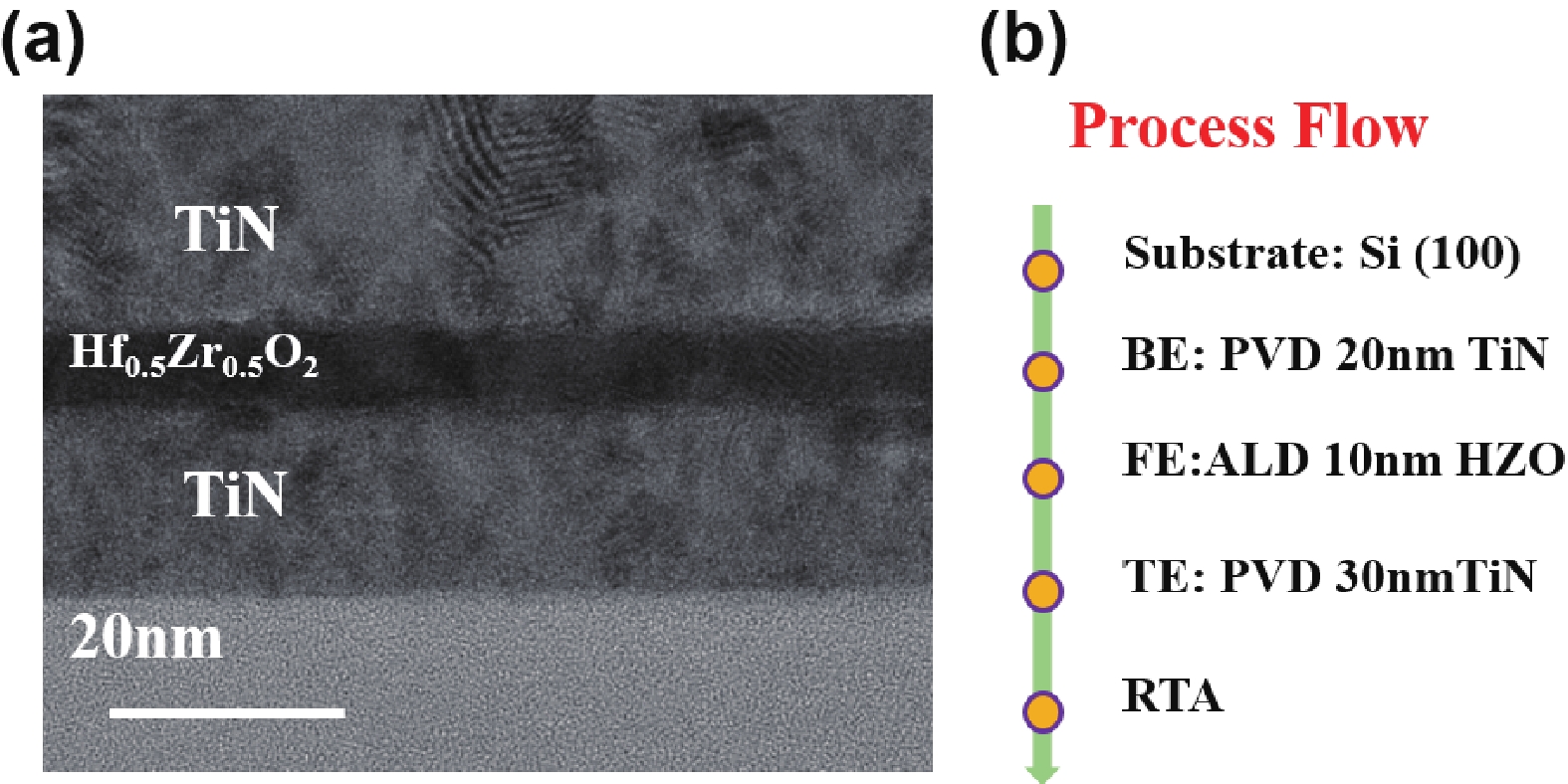
FE-HfO2 capacitor were grown on Si (100) wafer. Fig. 3(a) shows the TEM image of the TiN/HZO/TiN capacitor. The fabrication process of FE devices is as follow (Fig. 3(b)): Firstly, a 20-nm thick TiN bottom electrode (BE) were deposited via physical vapor deposition (PVD) method. Subsequently, 10 nm HZO film were deposited by atomic layer deposition (ALD) at 280 ℃ with a Hf : Zr ratio of 1 : 1 as followed. TEMAH, TEMAZ, and H2O were served as Hf-precursor, Zr-precursor, and oxygen source, respectively. Latterly, 30-nm thick patterned TiN were deposited via PVD method as top electrode (TE). 40 μm × 40 μm dimension square TEs were utilized for electrical tests. At the end, both HZO capacitors were annealed at 500 ℃ for 60 s in N2 atmosphere using a rapid thermal annealing system (RTA).

Fig. 3.  (Color online) (a) The TEM image of the TiN/HZO/TiN capacitor. (b) The fabrication process of FE devices.

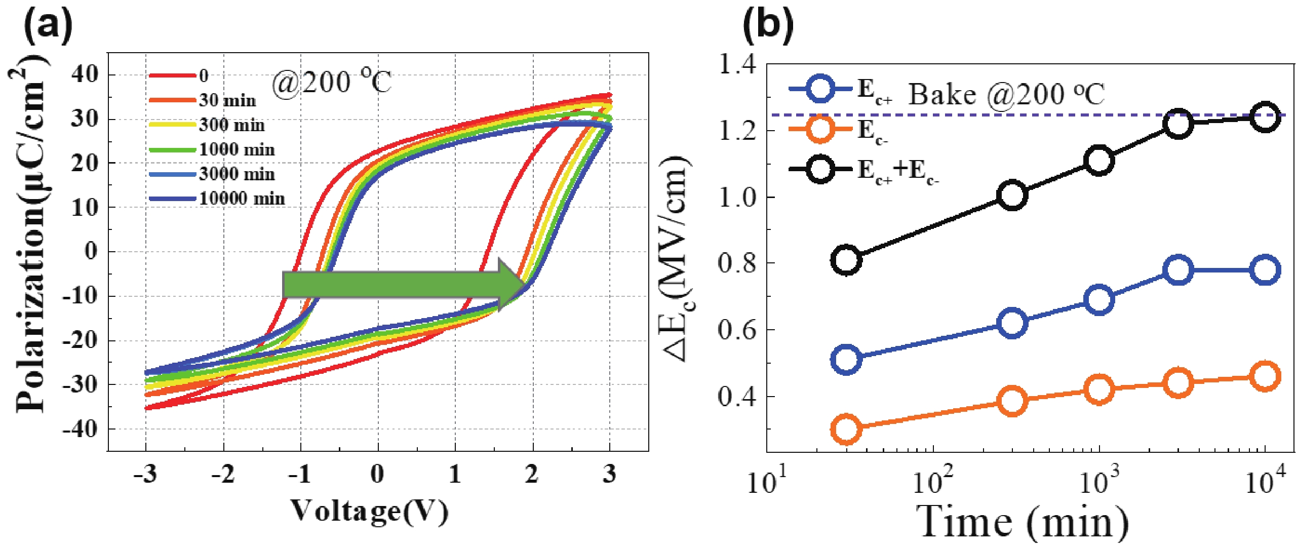
When evaluating FRAM retention reliability, imprint is the most important retention reliability mechanism for FRAM[11, 12]. Ferroelectric memories experience more imprint when exposed to higher temperatures and longer periods of time. However, the limit of imprint in FE-HfO2 has not evaluated yet. To this end, we selected a 10 nm HZO capacitor which was subjected to baking at 200 ℃ for prolonged test. As shown in Fig. 4, for 10 nm HZO device, Ec gradually shifts towards the positive direction as the baking time was prolonged, and exponential growth of ∆Ec was observed within 3000 min due to the high baking temperature. However, limit imprint was discovered when the baking time was as long as 104 min. The observed phenomenon can be understood by the imprint explanation in our previous work[11]. It is shown that oxygen vacancies near the interface between the dielectric and electrode are at the heart of imprint in HZO. Since oxygen vacancies were unavoidably generated during the growth processes e.g., element diffusion during thermal annealing, physical bombardment during sputtering top electrode, thus, imprint is inevitably appearing. Nevertheless, the amount of oxygen vacancies in HZO film is limited and will not increase during baking, even though the baking time was increasing to 104 min. It should be noted that although Ec shift by imprint has a limit, it was obtained by baking at a high temperature of 200 ℃ for over 10 000 min, indicating that imprint has always existed in ferroelectric memories and is an inevitable phenomenon.

Fig. 4.  (Color online) High temperature imprint test at 200 ℃ for TiN/HZO/TiN capacitors. (a) The corresponding P−V loops for HZO devices after different baking time from 0−10 000 min. (b) Evolution of extracted ∆Ec vs baking time.

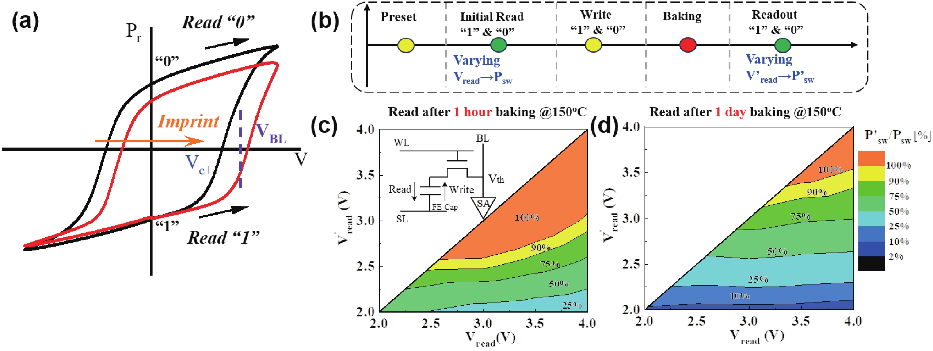
To further investigate the impact of imprint on the read and write operations for FeRAM, electrical test was conducted. Fig. 5 represents typical read and write operation of 1T1C FeRAM storage units. Considering the capacitor polarization state will not change when logic "0" is read, only the impact of imprint on logic "1" is considered here. Usually, the D-value in polarization between "0" and "1" of FeRAM is defined as the memory window. Hence, considering the reliability issue caused by imprint, we further investigated the degradation of the FeRAM memory in high temperature. In order to investigate the influence of the imprint on ferroelectric devices with different operating voltages, we simulated the reading and writing of FeRAM using ferroelectric capacitors and conducted retention tests. As shown in Fig. 5 (b), each sample was subjected to 1000 cycles to wake up, before sent to the baking test. After that, multiple amplitude pulses (Vread and V’read) were conducted to HZO devices before and after baking in order to obtain the switching polarization (Psw and P’sw) logic "1" state. As the baking time increases, which is shown in Figs. 5(c) and 5(d), the subsequent read "1" operation shows a decrease in remanent polarization, and a significant degradation of the memory window is observed. Therefore, for memory application with low voltage operations or multilevel storage, imprint is a significant threat. Only by increasing the read voltage can the impact of imprint be reduced.

Fig. 5.  (Color online) (a) Schematic diagram of hysteresis loop of a FE capacitor caused by imprint. (b) Baking testing scheme for ferroelectric devices with different operating voltages. (c) and (d) Comparison of switching polarization of ferroelectric capacitors before and after baking. The pronounced degradation of the FeRAM memory is observed for low operation voltage devices in high temperature.

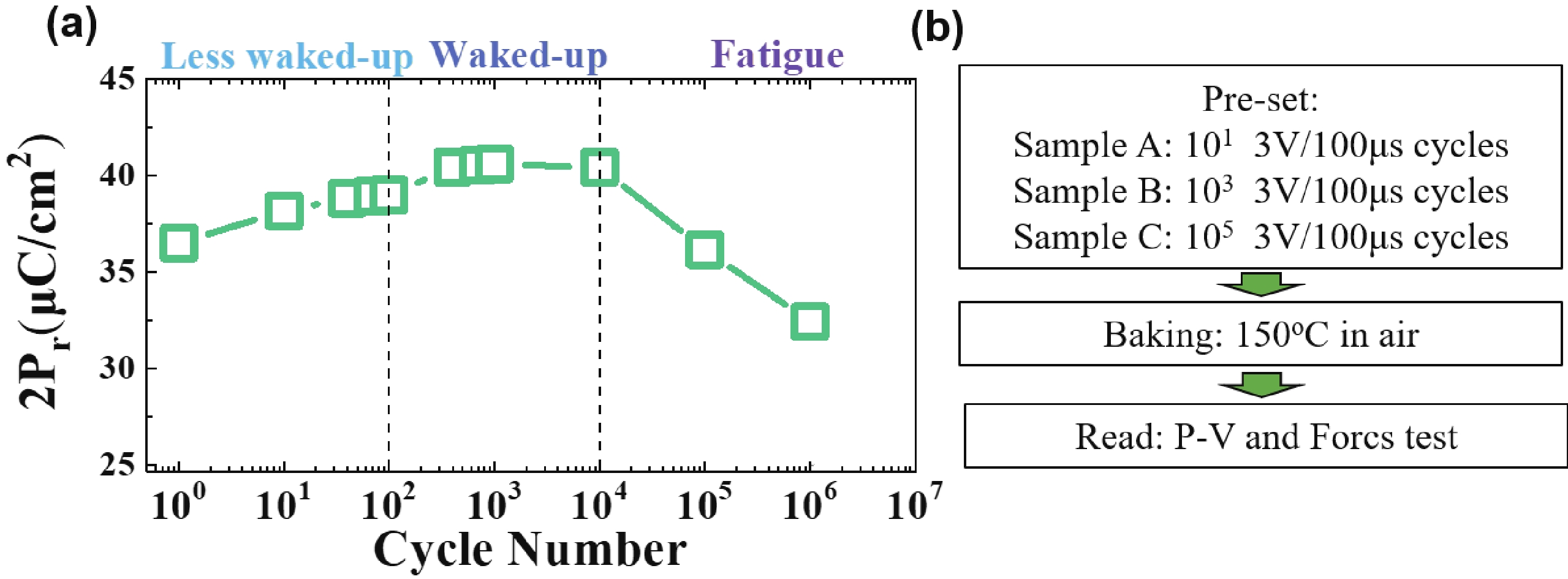
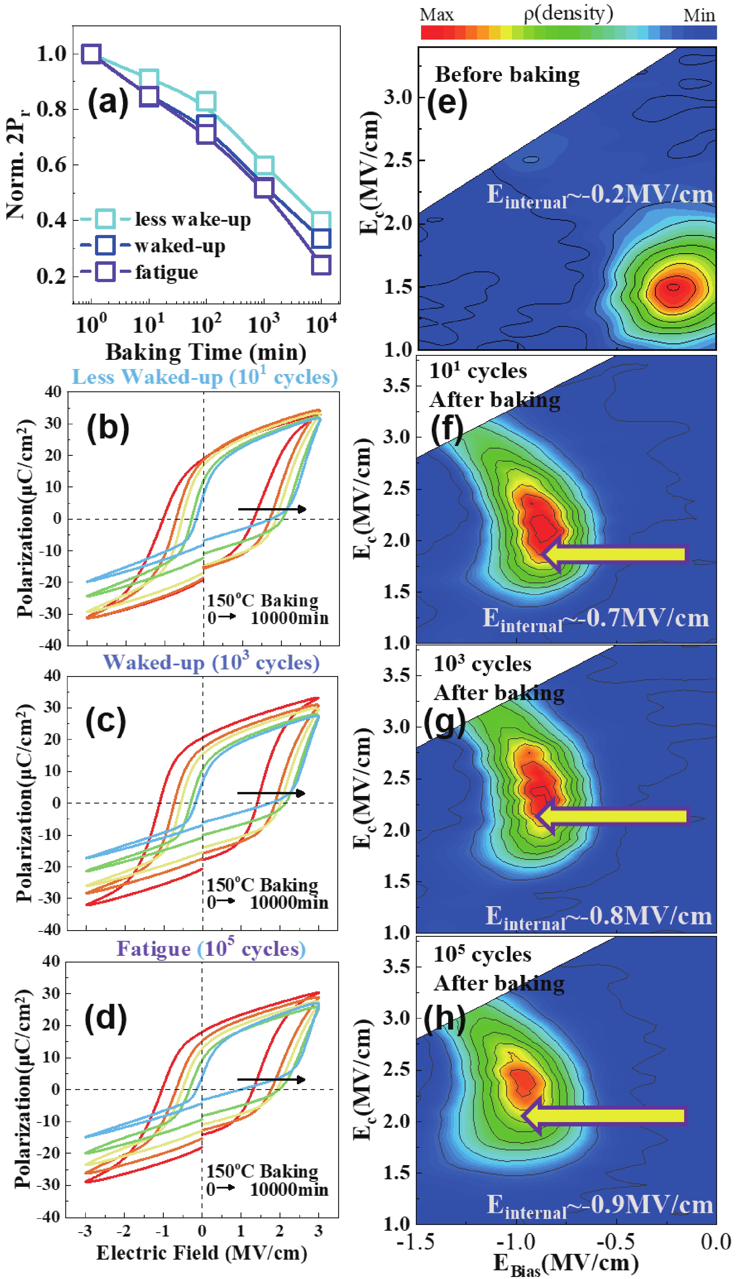
Besides imprint effect, wake-up effect and fatigue, which occur in different cycles period, are also critical reliability issues in ferroelectric capacitors[1316]. Usually, as shown in Fig. 6(a), with the number of cycles increases, HZO FE capacitors exhibit three states: 1) Waking-up state—the polarization of HZO devices increases with cycling operation due to the redistribution of oxygen vacancies or the transformation of tetragonal phases into orthogonal phases[13, 14]; 2) Waked-up state—The polarization of FE devices remains relatively stable as the number of cycles increases; 3) Fatigue state—Stress gradually accumulates, generating oxygen vacancies at grain boundaries, leading to a decrease in polarization and an increase in leakage[15, 16]. Typically, imprint measurements were conducted by using waked-up FE devices[17, 18]. However, the measurement of imprint for HZO capacitors during the waking-up and fatigue states has not been evaluated yet. To the end, three devices with different pre-cycles (101, 103, and 105 cycles) are tested as shown in Fig. 6(b). After pre-set, both samples were baked at 150 ℃ in air atmosphere for a period of time to accelerate the imprint and Ec shift. First order reversal curves (FORCs) were carried out for the devices before and after 103 min baking at 150 ℃. FORCs test is used to measure the coercive field and internal electric field (Einternal) inside ferroelectric capacitors, which is suitable to detect the change of Einternal caused by imprint[19, 20]. Fig. 7 shows the correlation between the imprint and number of cycles before baking. As Figs. 7(b)−7(d) show the P−V hysteresis loops of the MFM capacitor with 10 nm HZO film before and after high-temperature annealing. It can be observed for all samples that Ec gradually shifts towards the positive direction and the Pr decreases drastically as the baking time was prolonged. This Ec shift and Pr decrease is more pronounced in the cases of fatigue state devices according to the statistics in Fig. 7(a). The corresponding FORCs measurements after 1000 min, 150 ℃ annealing for three cases are illustrated in Figs. 7(e)−7(h). As shown in Fig. 7(e), the switching densities for unbaked devices is concentrated around −0.2 MV/cm (EBias), which is related to different deposition condition for TE and BE. After high temperature annealing, internal electric field shifted to negative direction for both samples, and EBias is located near −0.7, −0.8 and −0.9 MV/cm for less waked-up samples, and well waked-up samples and fatigued samples, respectively (Figs. 7(f)−7(h)). This observed phenomenon is supporting the wake-up and fatigue explanation[1214], since cycling operation inevitably causes changes in the number or state of oxygen vacancies which is the role of imprint in HZO ferroelectric thin films.

Fig. 6.  (Color online) Evolution of remanent polarization with electric field cycling using rectangular pulses. The HZO FE capacitors exhibit three states: Less waked-up, waked-up and fatigue. (b) Imprint test flow for three samples.
Fig. 7.  (Color online) (a) ∆Ec as a function of baking time with different number of cycles before bake when the FE device is fatigued, the degree of imprint was worse. (b)−(d) P−V hysteresis loops of the MFM capacitor with 10 nm HZO film before and after high-temperature annealing. (e)−(h) The corresponding FORCs measurements after 1000 min at 150 ℃ annealing for three cases.

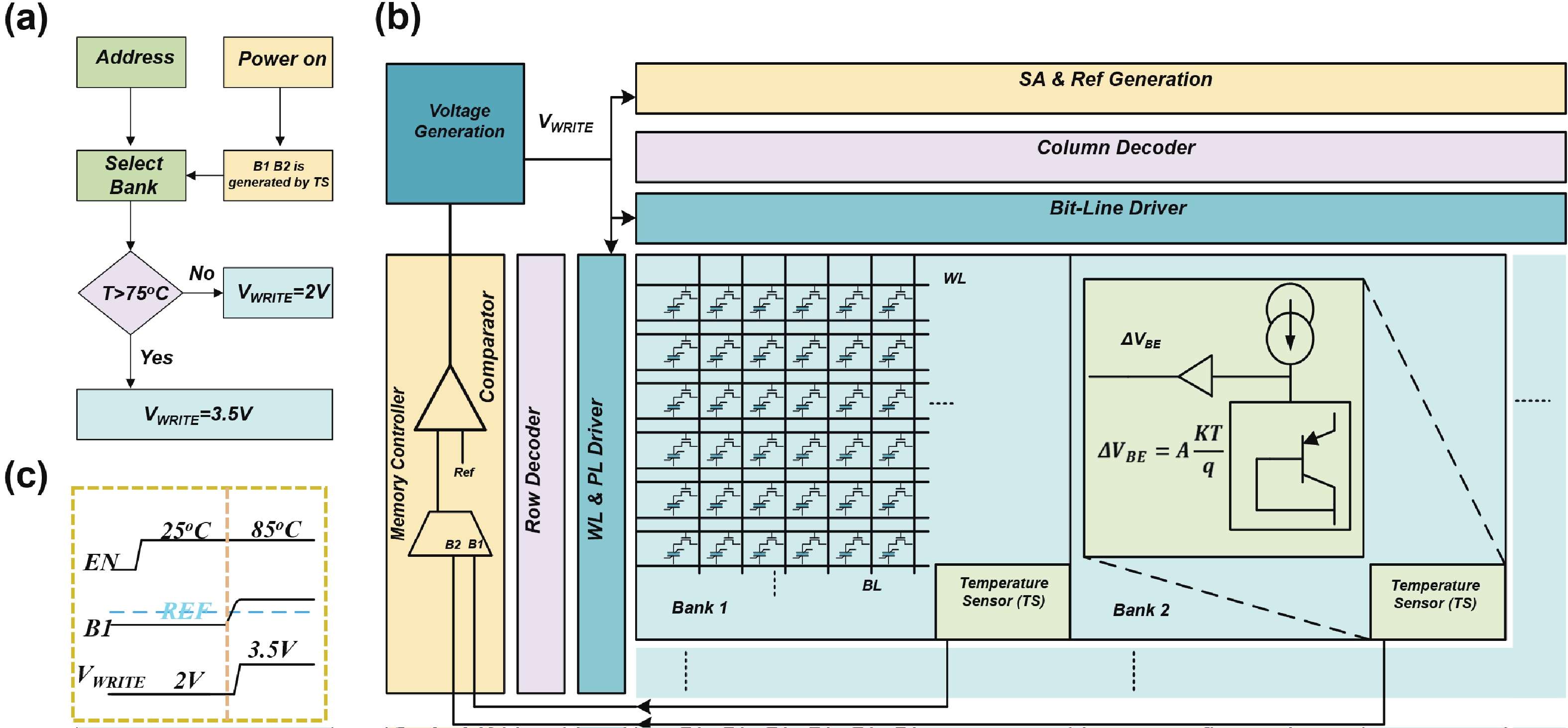
To get rid of the Ec shift and polarization degradation caused by imprint effect, a sensing circuit is designed to overcome the misreading problem as shown in Fig. 8(a). This circuit can detect the ambient temperature of the FE capacitor, and adjust the Vwrite according to the temperature. The array is divided into multiple banks and a temperature sensor circuit is added in each bank to better sense the temperature change, as shown in Fig. 8(b). The temperature sensing circuit is designed based on the temperature characteristics of CMOS parasitic diode, which can generate a voltage proportional to temperature. After power-on, the temperature sensor in each bank is activated to generate the temperature signal such as B1, which is then input into a MUX. Memory control selects the temperature signal voltage of the bank according to the address of the target cell being operated, and was compared with the reference voltage. If the temperature is greater than 75 ℃, the working voltage is 3.5 V, otherwise it is 2 V as demonstrated in Fig. 8(c). This solution is simple, fast and low-cost, and can effectively solve the misreading problem caused by the imprint of FE capacitors.

Fig. 8.  (Color online) The proposed sensing circuit to overcome the misreading problem. (a) and (b) Schematics of the solution and the circuit. (c) The working temperature of the selected Bank 1 changes from 25 to 85 ℃ and the write voltage then changes from 2 to 3.5 V.

In this work, the relationship between imprint and reliability of HZO-based FeRAM is systematically studied. Based on the electrical tests on extreme high temperature, imprint exists a limit in HZO capacitors but difficult to achieve. Imprint have a significant influence on the retention characteristics of the ferroelectric memory by reducing the memory window. Furthermore, imprint effect is observed during all cycling period, and is more serious in fatigue state. Based on the results, we have proposed a practical solution which could suppress the reliability degradation induced by imprint significantly.

This research was supported by the National Key R&D Program of China (Grant No. 2022YFB3606900), and in part by the National Natural Science of China (Grant No. 62004217).


[1]
Park M H, Lee Y H, Kim H J, et al. Ferroelectricity and antiferroelectricity of doped thin HfO2-based films. Adv Mater, 2015, 27, 1811 doi: 10.1002/adma.201404531
[2]
Schroeder U, Park M H, Mikolajick T, et al. The fundamentals and applications of ferroelectric HfO2. Nat Rev Mater, 2022, 7, 653 doi: 10.1038/s41578-022-00431-2
[3]
Fan Z, Chen J S, Wang J. Ferroelectric HfO2-based materials for next-generation ferroelectric memories. J Adv Dielect, 2016, 6, 1630003 doi: 10.1142/S2010135X16300036
[4]
Böscke T S, Müller J, Bräuhaus D, et al. Ferroelectricity in hafnium oxide thin films. Appl Phys Lett, 2011, 99, 102903. doi: 10.1063/1.3634052
[5]
Park M H, Lee Y H, Mikolajick T, et al. Review and perspective on ferroelectric HfO2-based thin films for memory applications. MRS Commun, 2018, 8, 795 doi: 10.1557/mrc.2018.175
[6]
Ali T, Polakowski P, Kühnel K, et al. A multilevel FeFET memory device based on laminated HSO and HZO ferroelectric layers for high-density storage. 2019 IEEE International Electron Devices Meeting (IEDM), 2019, 28.7. 1 doi: 10.1109/IEDM19573.2019.8993642
[7]
Sharma A, Roy K. Design space exploration of hysteresis-free HfZrOx-based negative capacitance FETs. IEEE Electron Device Lett, 2017, 38, 1165 doi: 10.1109/LED.2017.2714659
[8]
Okuno J, Kunihiro T, Konishi K, et al. 1T1C FeRAM memory array based on ferroelectric HZO with capacitor under bitline. IEEE J Electron Devices Soc, 2021, 10, 29 doi: 10.1109/JEDS.2021.3129279
[9]
Francois T, Grenouillet L, Coignus J, et al. Demonstration of BEOL-compatible ferroelectric Hf0.5Zr0.5O2 scaled FeRAM co-integrated with 130nm CMOS for embedded NVM applications. 2019 IEEE International Electron Devices Meeting (IEDM), 2019, 15.7. 1 doi: 10.1109/IEDM19573.2019.8993485
[10]
Kuk S H, Han S M, Kim B H, et al. An investigation of HZO-based n/p-FeFET operation mechanism and improved device performance by the electron detrapping mode. IEEE Trans Electron Devices, 2022, 69, 2080 doi: 10.1109/TED.2022.3154687
[11]
Zhou Y, Chan H K, Lam C H, et al. Mechanisms of imprint effect on ferroelectric thin films. J Appl Phys, 2005, 98, 024111. doi: 10.1063/1.1984075
[12]
Yuan P, Mao G Q, Cheng Y, et al. Microscopic mechanism of imprint in hafnium oxide-based ferroelectrics. Nano Res, 2022, 15, 3667 doi: 10.1007/s12274-021-4047-y
[13]
Jiang P F, Luo Q, Xu X X, et al. Wake-up effect in HfO2-based ferroelectric films. Adv Elect Materials, 2021, 7, 2000728 doi: 10.1002/aelm.202000728
[14]
Zhou Y, Zhang Y K, Yang Q, et al. The effects of oxygen vacancies on ferroelectric phase transition of HfO2-based thin film from first-principle. Comput Mater Sci, 2019, 167, 143 doi: 10.1016/j.commatsci.2019.05.041
[15]
Cheng Y, Gao Z M, Ye K H, et al. Reversible transition between the polar and antipolar phases and its implications for wake-up and fatigue in HfO2-based ferroelectric thin film. Nat Commun, 2022, 13, 645 doi: 10.1038/s41467-022-28236-5
[16]
Grimley E D, Schenk T, Sang X H, et al. Structural changes underlying field-cycling phenomena in ferroelectric HfO2 thin films. Adv Elect Materials, 2016, 2, 1600173 doi: 10.1002/aelm.201600173
[17]
Sünbül A, Lehninger D, Lederer M, et al. A study on imprint behavior of ferroelectric hafnium oxide caused by high-temperature annealing. Phys Status Solidi A, 2023, 220, 2300067. doi: 10.1002/pssa.202300067
[18]
Bao K Y, Liao J J, Yan F, et al. Enhanced endurance and imprint properties in Hf0.5Zr0.5O2– δ ferroelectric capacitors by tailoring the oxygen vacancy. ACS Appl Electron Mater, 2023, 5, 4615 doi: 10.1021/acsaelm.3c00756
[19]
Yuan P, Wang B P, Yang Y, et al. Enhanced remnant polarization (30 μC/cm2) and retention of ferroelectric Hf0.5Zr0.5O2 by NH3 plasma treatment. IEEE Electron Device Lett, 2022, 43, 1045 doi: 10.1109/LED.2022.3178867
[20]
Nie B W, Huang Y Q, Wang Y, et al. Thermal induced Pr degradation under low-voltage operation in HfZrO ferroelectric film: Phenomenon and underlying mechanism. IEEE Electron Device Lett, 2023, 44, 1456 doi: 10.1109/LED.2023.3296797
Fig. 1.  (Color online) (a) The schematic diagram of the typical FeRAM 1T−1C array, in which the transistors are controlled by WLs and the ferroelectric capacitors are controlled by PLs and BLs. (b) The readout circuit of the FeRAM 1T−1C bit-cell. (c) Timing diagrams for the read operation scheme of the 1T1C FeRAM cell for data "0" and data "1". Misreading occurs at high temperature (100 ℃).

Fig. 2.  (Color online) (a) and (b) The sensing current and corresponding charge for bits "1" during read operations at 25 and 100 ℃. (c) For FE devices, pronounced reduction in switching polarization signal reading at elevated temperature is observed. The sense margin may decrease when operating at high temperature (100 ℃).

Fig. 3.  (Color online) (a) The TEM image of the TiN/HZO/TiN capacitor. (b) The fabrication process of FE devices.

Fig. 4.  (Color online) High temperature imprint test at 200 ℃ for TiN/HZO/TiN capacitors. (a) The corresponding P−V loops for HZO devices after different baking time from 0−10 000 min. (b) Evolution of extracted ∆Ec vs baking time.

Fig. 5.  (Color online) (a) Schematic diagram of hysteresis loop of a FE capacitor caused by imprint. (b) Baking testing scheme for ferroelectric devices with different operating voltages. (c) and (d) Comparison of switching polarization of ferroelectric capacitors before and after baking. The pronounced degradation of the FeRAM memory is observed for low operation voltage devices in high temperature.

Fig. 6.  (Color online) Evolution of remanent polarization with electric field cycling using rectangular pulses. The HZO FE capacitors exhibit three states: Less waked-up, waked-up and fatigue. (b) Imprint test flow for three samples.

Fig. 7.  (Color online) (a) ∆Ec as a function of baking time with different number of cycles before bake when the FE device is fatigued, the degree of imprint was worse. (b)−(d) P−V hysteresis loops of the MFM capacitor with 10 nm HZO film before and after high-temperature annealing. (e)−(h) The corresponding FORCs measurements after 1000 min at 150 ℃ annealing for three cases.

Fig. 8.  (Color online) The proposed sensing circuit to overcome the misreading problem. (a) and (b) Schematics of the solution and the circuit. (c) The working temperature of the selected Bank 1 changes from 25 to 85 ℃ and the write voltage then changes from 2 to 3.5 V.

[1]
Park M H, Lee Y H, Kim H J, et al. Ferroelectricity and antiferroelectricity of doped thin HfO2-based films. Adv Mater, 2015, 27, 1811 doi: 10.1002/adma.201404531
[2]
Schroeder U, Park M H, Mikolajick T, et al. The fundamentals and applications of ferroelectric HfO2. Nat Rev Mater, 2022, 7, 653 doi: 10.1038/s41578-022-00431-2
[3]
Fan Z, Chen J S, Wang J. Ferroelectric HfO2-based materials for next-generation ferroelectric memories. J Adv Dielect, 2016, 6, 1630003 doi: 10.1142/S2010135X16300036
[4]
Böscke T S, Müller J, Bräuhaus D, et al. Ferroelectricity in hafnium oxide thin films. Appl Phys Lett, 2011, 99, 102903. doi: 10.1063/1.3634052
[5]
Park M H, Lee Y H, Mikolajick T, et al. Review and perspective on ferroelectric HfO2-based thin films for memory applications. MRS Commun, 2018, 8, 795 doi: 10.1557/mrc.2018.175
[6]
Ali T, Polakowski P, Kühnel K, et al. A multilevel FeFET memory device based on laminated HSO and HZO ferroelectric layers for high-density storage. 2019 IEEE International Electron Devices Meeting (IEDM), 2019, 28.7. 1 doi: 10.1109/IEDM19573.2019.8993642
[7]
Sharma A, Roy K. Design space exploration of hysteresis-free HfZrOx-based negative capacitance FETs. IEEE Electron Device Lett, 2017, 38, 1165 doi: 10.1109/LED.2017.2714659
[8]
Okuno J, Kunihiro T, Konishi K, et al. 1T1C FeRAM memory array based on ferroelectric HZO with capacitor under bitline. IEEE J Electron Devices Soc, 2021, 10, 29 doi: 10.1109/JEDS.2021.3129279
[9]
Francois T, Grenouillet L, Coignus J, et al. Demonstration of BEOL-compatible ferroelectric Hf0.5Zr0.5O2 scaled FeRAM co-integrated with 130nm CMOS for embedded NVM applications. 2019 IEEE International Electron Devices Meeting (IEDM), 2019, 15.7. 1 doi: 10.1109/IEDM19573.2019.8993485
[10]
Kuk S H, Han S M, Kim B H, et al. An investigation of HZO-based n/p-FeFET operation mechanism and improved device performance by the electron detrapping mode. IEEE Trans Electron Devices, 2022, 69, 2080 doi: 10.1109/TED.2022.3154687
[11]
Zhou Y, Chan H K, Lam C H, et al. Mechanisms of imprint effect on ferroelectric thin films. J Appl Phys, 2005, 98, 024111. doi: 10.1063/1.1984075
[12]
Yuan P, Mao G Q, Cheng Y, et al. Microscopic mechanism of imprint in hafnium oxide-based ferroelectrics. Nano Res, 2022, 15, 3667 doi: 10.1007/s12274-021-4047-y
[13]
Jiang P F, Luo Q, Xu X X, et al. Wake-up effect in HfO2-based ferroelectric films. Adv Elect Materials, 2021, 7, 2000728 doi: 10.1002/aelm.202000728
[14]
Zhou Y, Zhang Y K, Yang Q, et al. The effects of oxygen vacancies on ferroelectric phase transition of HfO2-based thin film from first-principle. Comput Mater Sci, 2019, 167, 143 doi: 10.1016/j.commatsci.2019.05.041
[15]
Cheng Y, Gao Z M, Ye K H, et al. Reversible transition between the polar and antipolar phases and its implications for wake-up and fatigue in HfO2-based ferroelectric thin film. Nat Commun, 2022, 13, 645 doi: 10.1038/s41467-022-28236-5
[16]
Grimley E D, Schenk T, Sang X H, et al. Structural changes underlying field-cycling phenomena in ferroelectric HfO2 thin films. Adv Elect Materials, 2016, 2, 1600173 doi: 10.1002/aelm.201600173
[17]
Sünbül A, Lehninger D, Lederer M, et al. A study on imprint behavior of ferroelectric hafnium oxide caused by high-temperature annealing. Phys Status Solidi A, 2023, 220, 2300067. doi: 10.1002/pssa.202300067
[18]
Bao K Y, Liao J J, Yan F, et al. Enhanced endurance and imprint properties in Hf0.5Zr0.5O2– δ ferroelectric capacitors by tailoring the oxygen vacancy. ACS Appl Electron Mater, 2023, 5, 4615 doi: 10.1021/acsaelm.3c00756
[19]
Yuan P, Wang B P, Yang Y, et al. Enhanced remnant polarization (30 μC/cm2) and retention of ferroelectric Hf0.5Zr0.5O2 by NH3 plasma treatment. IEEE Electron Device Lett, 2022, 43, 1045 doi: 10.1109/LED.2022.3178867
[20]
Nie B W, Huang Y Q, Wang Y, et al. Thermal induced Pr degradation under low-voltage operation in HfZrO ferroelectric film: Phenomenon and underlying mechanism. IEEE Electron Device Lett, 2023, 44, 1456 doi: 10.1109/LED.2023.3296797
  • Search

    Advanced Search >>

    GET CITATION

    shu

    Export: BibTex EndNote

    Article Metrics

    Article views: 1566 Times PDF downloads: 210 Times Cited by: 0 Times

    History

    Received: 17 October 2023 Revised: 28 December 2023 Online: Accepted Manuscript: 05 January 2024Uncorrected proof: 10 January 2024Published: 10 April 2024

    Catalog

      Email This Article

      User name:
      Email:*请输入正确邮箱
      Code:*验证码错误
      Peng Yuan, Yuting Chen, Liguo Chai, Zhengying Jiao, Qingjie Luan, Yongqing Shen, Ying Zhang, Jibin Leng, Xueli Ma, Jinjuan Xiang, Guilei Wang, Chao Zhao. On the relationship between imprint and reliability in Hf0.5Zr0.5O2 based ferroelectric random access memory[J]. Journal of Semiconductors, 2024, 45(4): 042301. doi: 10.1088/1674-4926/45/4/042301 ****P Yuan, Y T Chen, L G Chai, Z Y Jiao, Q J Luan, Y Q Shen, Y Zhang, J B Leng, X L Ma, J J Xiang, G L Wang, C Zhao. On the relationship between imprint and reliability in Hf0.5Zr0.5O2 based ferroelectric random access memory[J]. J. Semicond, 2024, 45(4): 042301. doi: 10.1088/1674-4926/45/4/042301
      Citation:
      Peng Yuan, Yuting Chen, Liguo Chai, Zhengying Jiao, Qingjie Luan, Yongqing Shen, Ying Zhang, Jibin Leng, Xueli Ma, Jinjuan Xiang, Guilei Wang, Chao Zhao. On the relationship between imprint and reliability in Hf0.5Zr0.5O2 based ferroelectric random access memory[J]. Journal of Semiconductors, 2024, 45(4): 042301. doi: 10.1088/1674-4926/45/4/042301 ****
      P Yuan, Y T Chen, L G Chai, Z Y Jiao, Q J Luan, Y Q Shen, Y Zhang, J B Leng, X L Ma, J J Xiang, G L Wang, C Zhao. On the relationship between imprint and reliability in Hf0.5Zr0.5O2 based ferroelectric random access memory[J]. J. Semicond, 2024, 45(4): 042301. doi: 10.1088/1674-4926/45/4/042301

      On the relationship between imprint and reliability in Hf0.5Zr0.5O2 based ferroelectric random access memory

      DOI: 10.1088/1674-4926/45/4/042301
      More Information
      • Peng Yuan received his Ph.D. degree in Institute of Microelectronics, Chinese Academy of Sciences and University of Chinese Academy of Sciences. In 2022, he joined the Beijing Superstring Academy of Memory Technology as an assistant. His current research interests include high-k semiconductor materials and Emerging memory devices
      • Xueli Ma received her Ph.D. degree in Microelectronics and Solid-State Electronics from University of Chinese Academy of Sciences. She worked in the Institute of Microelectronics (IME), Chinese Academy of Sciences as an assistant professor and associate professor for 8 years. and joined SAMT at 2022. Her research interests cover high-k/metal gate stack of advanced CMOS, high-mobility channel SiGe/Ge-based processing and device technology, and oxide semiconductor-based TFTs. Emerging
      • Jinjuan Xiang received her Ph.D. degree in Microelectronics and Solid-State Electronics from University of Chinese Academy of Sciences. Her work focused on ALD process and material especially for Nano CMOS and DRAM application
      • Guilei Wang received his Bachelor's degree in 2005 and his PhD in 2016 from the University of Chinese Academy of Sciences. He has been worked as a professor at the Integrated Circuit Advanced Process Center at the Chinese Academy of Sciences until 2021. In October 2021, he joined the Beijing Superstring Academy of Memory Technology as a full professor. His research interests are focused on new materials, devices, and process integration for the IC industry
      • Corresponding author: Xueli.ma@bjsamt.org.cnJinjuan.Xiang@bjsamt.org.cnGuilei.Wang@bjsamt.org.cn
      • Received Date: 2023-10-17
      • Revised Date: 2023-12-28
      • Available Online: 2024-01-05

      Catalog

        /

        DownLoad:  Full-Size Img  PowerPoint
        Return
        Return