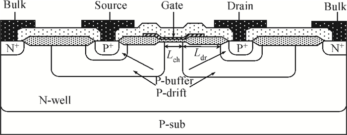
Fig. 1.
The schematic cross section of the investigated ps-LDMOS.
SEMICONDUCTOR DEVICES
Hao Wang, Siyang Liu, Weifeng Sun and Tingting Huang
Corresponding author: Sun Weifeng, Email:swffrog@seu.edu.cn
Abstract: The ESD response characteristic in a p-type symmetric lateral DMOS (ps-LDMOS) has been investigated. The experimental results show that the ps-LDMOS has weak ESD robustness due to an absence of the "snapback" characteristic. In addition, the location of the hot spot changes little for the special device. The method for reducing the lattice temperature of the hot spot can be used to enhance the ESD capacity of the ps-LDMOS, thereby, a novel and easily-achievable ps-LDMOS structure with a p-type lightly doped drain (p-LDD) has been proposed. The special region p-LDD lowers the electric field at the edge of the poly gate, making the whole distribution of the surface electric field more uniform. Therefore, the ESD robustness is improved two times and no obvious change of other electric parameters is introduced.
Key words: ESD response characteristic, ESD robustness, ps-LDMOS, p-LDD
| [1] |
Liu S, Sun W, Wan W, et al. The hot-carrier degradation mechanism of p-DDDMOS transistor with different p-drift dosage. IEEE International Conference of Electron Devices and Solid-State Circuits, 2011:1
|
| [2] |
Wang C T, Ker M D. ESD protection design with lateral DMOS transistor in 40-V BCD technology. IEEE Trans Electron Devices, 2010, 57(12):3395 doi: 10.1109/TED.2010.2079530
|
| [3] |
Chen W Y, Ker M D. Improving safe operating area of nLDMOS array with embedded silicon controlled rectifier for ESD protection in a 24-V BCD process. IEEE Trans Electron Devices, 2011, 58(9):2944 doi: 10.1109/TED.2011.2159861
|
| [4] |
Qian Q, Sun W, Wei S, et al. The investigation of electro-thermal characteristics of high-voltage lateral IGBT for ESD protection. IEEE Trans Device Mater Reliab, 2012, 12(1):146 doi: 10.1109/TDMR.2011.2178072
|
| [5] |
Zhu J, Qian Q, Sun W. A novel SOI IGBT for power-rail ESD clamp circuit. IEEE International Conference on Electron Devices and Solid-State Circuits, 2009:103 http://ieeexplore.ieee.org/document/5394178/
|
| [6] |
Song M, Cable J S, Woo J C S, et al. Optimization of LDD devices for cryogenic operation. IEEE Electron Device Lett, 1991, 12(7):375 doi: 10.1109/55.103612
|
| [7] |
Doyle B S, Mistry K R. Anomalous hot-carrier behavior for LDD p-channel transistors. IEEE Electron Device Lett, 1993, 14(11):536 doi: 10.1109/55.258007
|
| [8] |
Jie B B, Li M F, Lou C L, et al. Investigation of interface traps in LDD pMOST's by the DCIV method. IEEE Electron Device Lett, 1997, 18(12):583 doi: 10.1109/55.644078
|
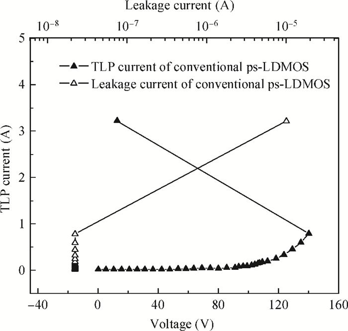
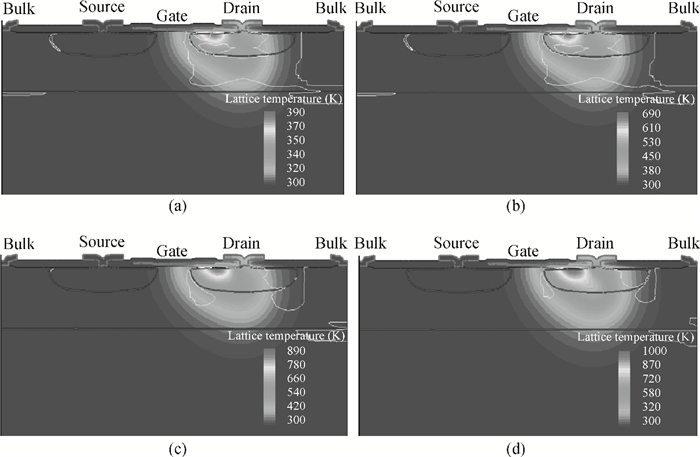
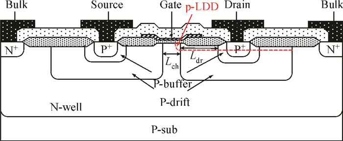
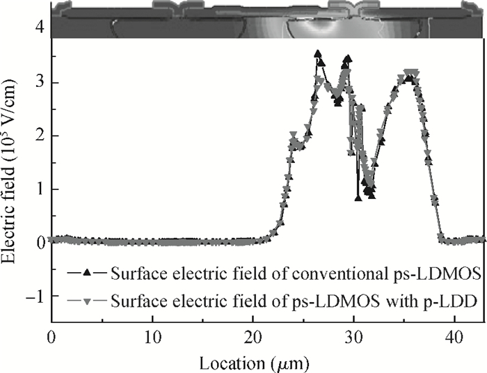
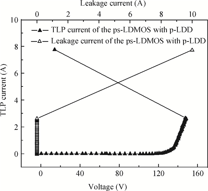
Table 1. The comparison of key parameters in the conventional and the novel ps-LDMOS.

|
| [1] |
Liu S, Sun W, Wan W, et al. The hot-carrier degradation mechanism of p-DDDMOS transistor with different p-drift dosage. IEEE International Conference of Electron Devices and Solid-State Circuits, 2011:1
|
| [2] |
Wang C T, Ker M D. ESD protection design with lateral DMOS transistor in 40-V BCD technology. IEEE Trans Electron Devices, 2010, 57(12):3395 doi: 10.1109/TED.2010.2079530
|
| [3] |
Chen W Y, Ker M D. Improving safe operating area of nLDMOS array with embedded silicon controlled rectifier for ESD protection in a 24-V BCD process. IEEE Trans Electron Devices, 2011, 58(9):2944 doi: 10.1109/TED.2011.2159861
|
| [4] |
Qian Q, Sun W, Wei S, et al. The investigation of electro-thermal characteristics of high-voltage lateral IGBT for ESD protection. IEEE Trans Device Mater Reliab, 2012, 12(1):146 doi: 10.1109/TDMR.2011.2178072
|
| [5] |
Zhu J, Qian Q, Sun W. A novel SOI IGBT for power-rail ESD clamp circuit. IEEE International Conference on Electron Devices and Solid-State Circuits, 2009:103 http://ieeexplore.ieee.org/document/5394178/
|
| [6] |
Song M, Cable J S, Woo J C S, et al. Optimization of LDD devices for cryogenic operation. IEEE Electron Device Lett, 1991, 12(7):375 doi: 10.1109/55.103612
|
| [7] |
Doyle B S, Mistry K R. Anomalous hot-carrier behavior for LDD p-channel transistors. IEEE Electron Device Lett, 1993, 14(11):536 doi: 10.1109/55.258007
|
| [8] |
Jie B B, Li M F, Lou C L, et al. Investigation of interface traps in LDD pMOST's by the DCIV method. IEEE Electron Device Lett, 1997, 18(12):583 doi: 10.1109/55.644078
|


Article views: 3643 Times PDF downloads: 37 Times Cited by: 0 Times
Received: 26 April 2013 Revised: 29 August 2013 Online: Published: 01 January 2014
| Citation: |
Hao Wang, Siyang Liu, Weifeng Sun, Tingting Huang. Research and optimization of the ESD response characteristic in a ps-LDMOS transistor[J]. Journal of Semiconductors, 2014, 35(1): 014010. doi: 10.1088/1674-4926/35/1/014010
****
H Wang, S Y Liu, W F Sun, T T Huang. Research and optimization of the ESD response characteristic in a ps-LDMOS transistor[J]. J. Semicond., 2014, 35(1): 014010. doi: 10.1088/1674-4926/35/1/014010.

|
| [1] |
Liu S, Sun W, Wan W, et al. The hot-carrier degradation mechanism of p-DDDMOS transistor with different p-drift dosage. IEEE International Conference of Electron Devices and Solid-State Circuits, 2011:1
|
| [2] |
Wang C T, Ker M D. ESD protection design with lateral DMOS transistor in 40-V BCD technology. IEEE Trans Electron Devices, 2010, 57(12):3395 doi: 10.1109/TED.2010.2079530
|
| [3] |
Chen W Y, Ker M D. Improving safe operating area of nLDMOS array with embedded silicon controlled rectifier for ESD protection in a 24-V BCD process. IEEE Trans Electron Devices, 2011, 58(9):2944 doi: 10.1109/TED.2011.2159861
|
| [4] |
Qian Q, Sun W, Wei S, et al. The investigation of electro-thermal characteristics of high-voltage lateral IGBT for ESD protection. IEEE Trans Device Mater Reliab, 2012, 12(1):146 doi: 10.1109/TDMR.2011.2178072
|
| [5] |
Zhu J, Qian Q, Sun W. A novel SOI IGBT for power-rail ESD clamp circuit. IEEE International Conference on Electron Devices and Solid-State Circuits, 2009:103 http://ieeexplore.ieee.org/document/5394178/
|
| [6] |
Song M, Cable J S, Woo J C S, et al. Optimization of LDD devices for cryogenic operation. IEEE Electron Device Lett, 1991, 12(7):375 doi: 10.1109/55.103612
|
| [7] |
Doyle B S, Mistry K R. Anomalous hot-carrier behavior for LDD p-channel transistors. IEEE Electron Device Lett, 1993, 14(11):536 doi: 10.1109/55.258007
|
| [8] |
Jie B B, Li M F, Lou C L, et al. Investigation of interface traps in LDD pMOST's by the DCIV method. IEEE Electron Device Lett, 1997, 18(12):583 doi: 10.1109/55.644078
|

 WeChat ID
Journal of Semiconductors © 2017 All Rights Reserved 京ICP备05085259号-2

 DownLoad: