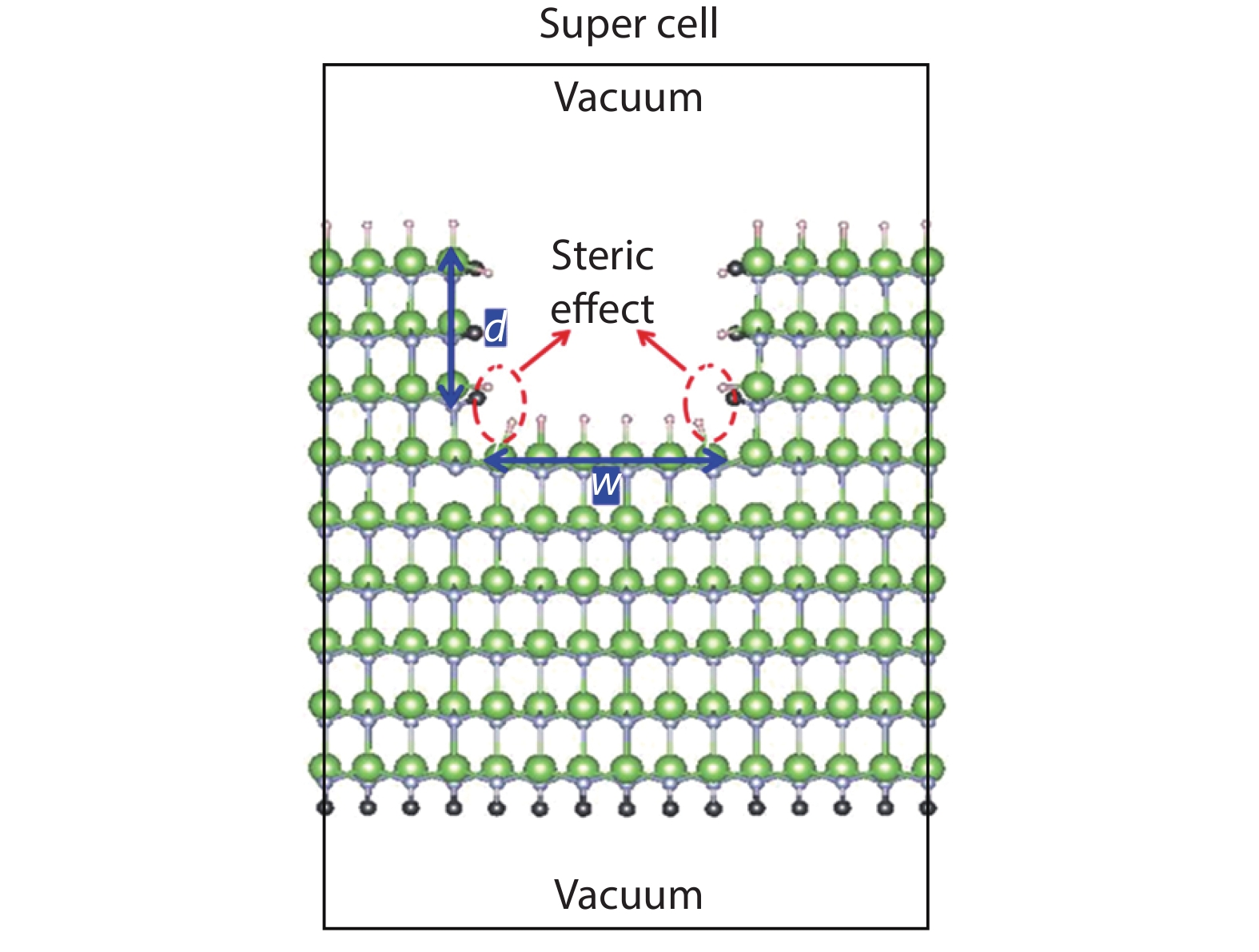
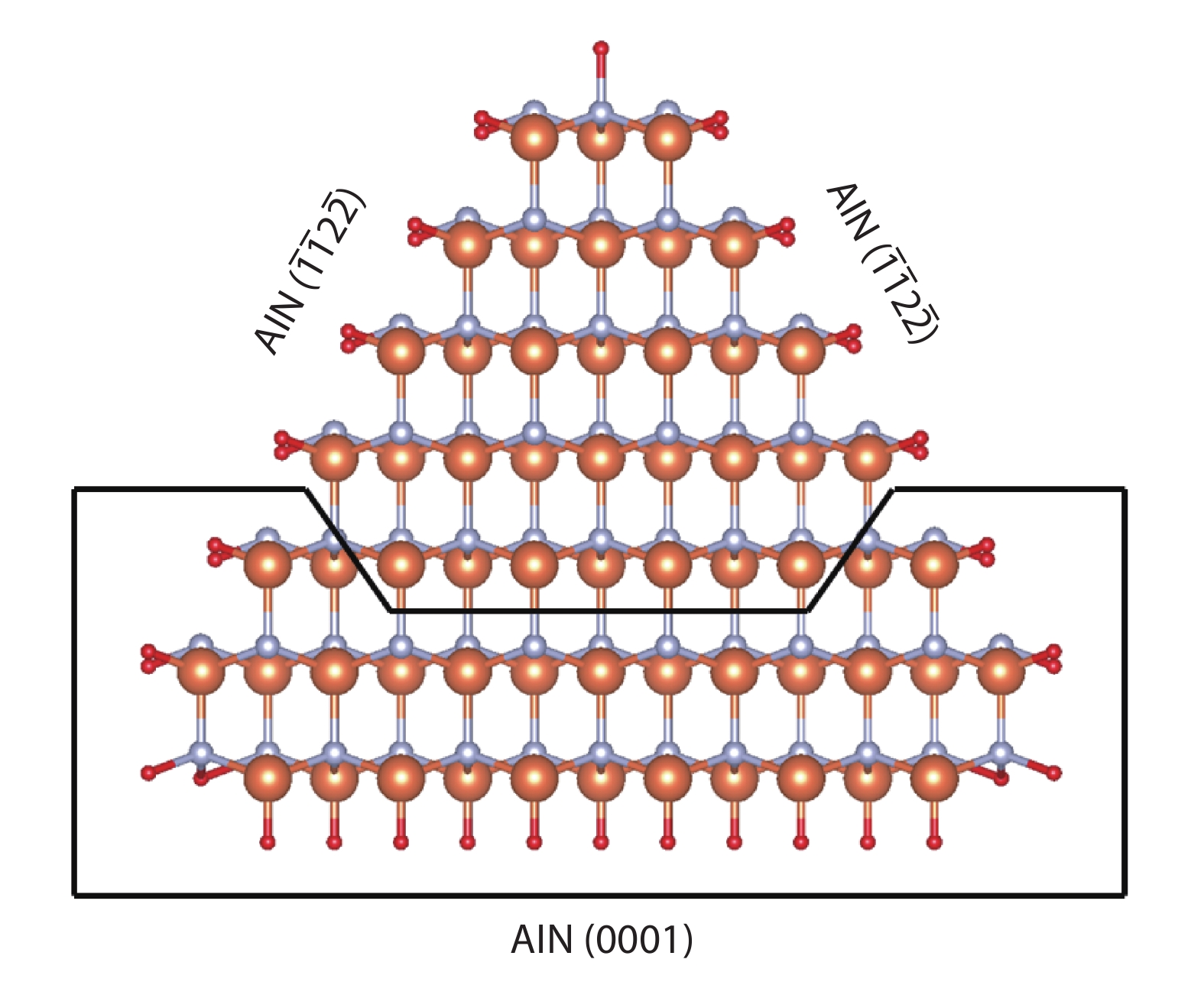
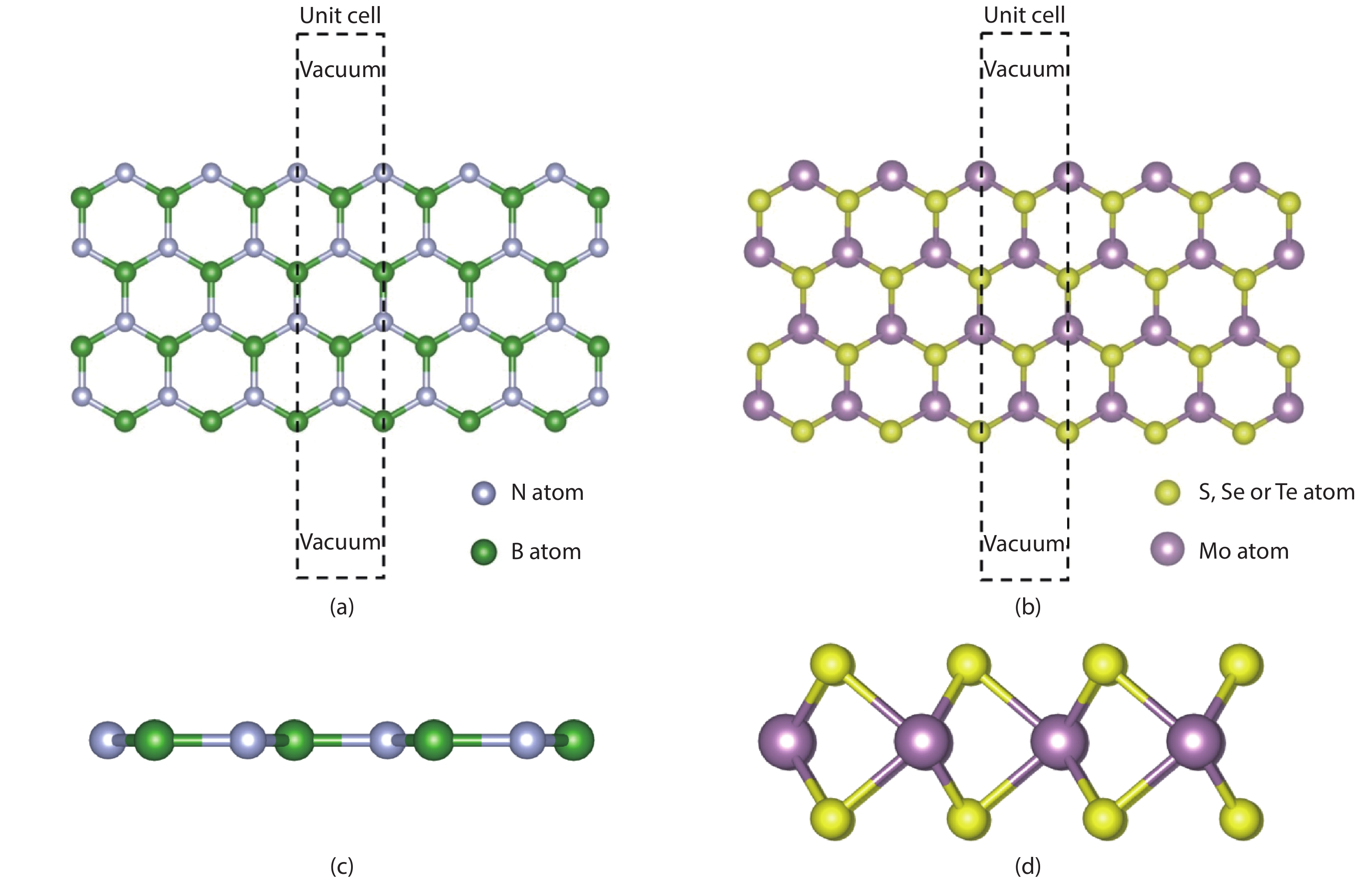
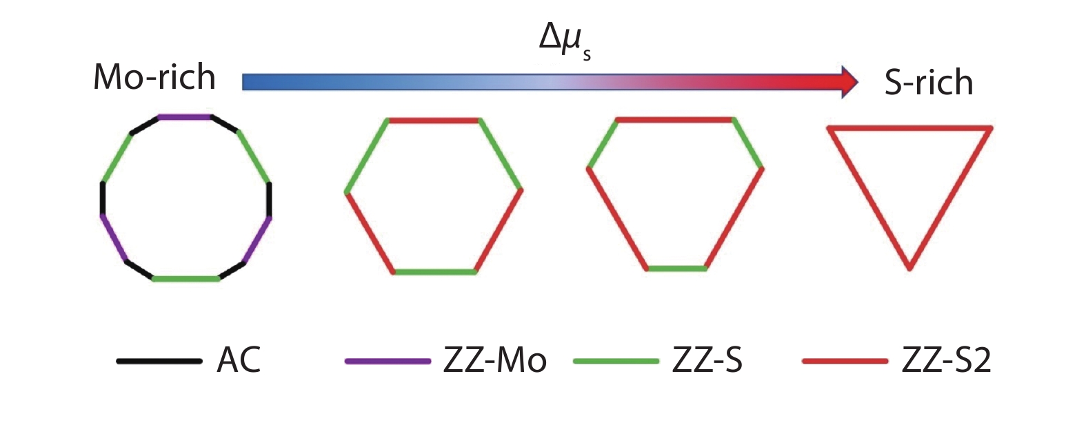
| [1] |
Bristowe N C, Littlewood P B, Artacho E. Surface defects and conduction in polar oxide heterostructures. J Phys B, 2011, 83, 205405 doi: 10.1103/PhysRevB.83.205405 |
| [2] |
Kahwaji S, Gordon R A, Crozier E D, et al. Surfactant-mediated growth of ferromagnetic Mn-doped Si. Phys Rev B, 2013, 88, 174419 doi: 10.1103/PhysRevB.88.174419 |
| [3] |
Zhang J, Zhao W, Zhu J. Missing links towards understanding the equilibrium shapes of hexagonal boron nitride: algorithm, hydrogen passivation, and temperature effects. Nanoscale, 2018, 10, 17683 doi: 10.1039/C8NR04732D |
| [4] |
Tang C, Spencer M J S, Barnard A S. Activity of ZnO polar surfaces: an insight from surface energies. Phys Chem Chem Phys, 2014, 16, 22139 doi: 10.1039/C4CP03221G |
| [5] |
Dingreville R, Qu J, Cherkaoui M. Surface free energy and its effect on the elastic behavior of nano-sized particles, wires and films. J Mech Phys Solids, 2005, 53, 1827 doi: 10.1016/j.jmps.2005.02.012 |
| [6] |
Gibbs J W, The collected works of J. Willard Gibbs. Longmans, Green, 1928
|
| [7] |
Wulff G. Xxv. zur frage der geschwindigkeit des wachsthums und der auflösung der krystallflächen. Zeitschrift für Kristallographie - Crystalline Materials, 1901, 34, 449
|
| [8] |
Curie M P. Sur la formation des cristaux et sur les constantes capillaires de leurs différentes faces. Bull Soc Fr Mineral, 1885, 8, 145
|
| [9] |
Li H, Geelhaar L, Riechert H, et al. Computing equilibrium shapes of wurtzite crystals: The example of GaN. Phys Rev Lett, 2015, 115, 085503 doi: 10.1103/PhysRevLett.115.085503 |
| [10] |
Lang N D, Kohn W. Theory of metal surfaces: Charge density and surface energy. Phys Rev B, 1970, 1, 4555 doi: 10.1103/PhysRevB.1.4555 |
| [11] |
Jaccodine R J. Surface energy of germanium and silicon. J Electrochem Soc, 1963, 110, 524 doi: 10.1149/1.2425806 |
| [12] |
Tyson W R, Miller W A. Surface free energies of solid metals: Estimation from liquid surface tension measurements. Surf Sci, 1977, 62, 267 doi: 10.1016/0039-6028(77)90442-3 |
| [13] |
de Boer F R, Boom R, Mattens W C M, et al. Cohesion in metals: Transition metal alloys. Elsevier Scientific Pub. Co., 1988
|
| [14] |
Bonzel H P, Emundts A. Absolute values of surface and step free energies from equilibrium crystal shapes. Phys Rev Lett, 2000, 84, 5804 doi: 10.1103/PhysRevLett.84.5804 |
| [15] |
Bonzel H P, Nowicki M. Absolute surface free energies of perfect low-index orientations of metals and semiconductors. Phys Rev B, 2004, 70, 245430 doi: 10.1103/PhysRevB.70.245430 |
| [16] |
Niessen A K, Miedema A R, de Boer F R, et al. Enthalpies of formation of liquid and solid binary alloys based on 3d metals: IV. alloys of cobalt. Physica B+C, 1988, 151, 401 doi: 10.1016/0378-4363(88)90296-3 |
| [17] |
Mills K C, Su Y C. Review of surface tension data for metallic elements and alloys: Part 1-pure metals. Int Mater Rev, 2006, 51, 329 doi: 10.1179/174328006X102510 |
| [18] |
Keene B J. Review of data for the surface tension of pure metals. Int Mater Rev, 1993, 38, 157 doi: 10.1179/imr.1993.38.4.157 |
| [19] |
Lee J Y, Punkkinen M, Schönecker S, et al. The surface energy and stress of metals. Surf Sci, 2018, 674, 51 doi: 10.1016/j.susc.2018.03.008 |
| [20] |
Perdew J P, Tran H Q, Smith E D. Stabilized jellium: Structureless pseudopotential model for the cohesive and surface properties of metals. Phys Rev B, 1990, 42, 11627 doi: 10.1103/PhysRevB.42.11627 |
| [21] |
Skriver H L, Rosengaard N M. Surface energy and work function of elemental metals. Phys Rev B, 1992, 46, 7157 doi: 10.1103/PhysRevB.46.7157 |
| [22] |
Erschbaumer H, Freeman A J, Fu C L, et al. Surface states, electronic structure and surface energy of the Ag (001) surface. Surf Sci, 1991, 243, 317 doi: 10.1016/0039-6028(91)90369-4 |
| [23] |
Needs R J, Mansfield M. Calculations of the surface stress tensor and surface energy of the (111) surfaces of iridium, platinum and gold. J Phys Condens Matter, 1989, 1, 41 doi: 10.1088/0953-8984/1/41/006 |
| [24] |
|
| [25] |
Galanakis I, Papanikolaou N, Dederichs P H. Applicability of the broken-bond rule to the surface energy of the fcc metals. Surf Sci, 2002, 511, 1 doi: 10.1016/S0039-6028(02)01547-9 |
| [26] |
Methfessel M, Hennig D, Scheffler M. Trends of the surface relaxations, surface energies, and work functions of the 4d transition metals. Phys Rev B, 1992, 46, 4816 doi: 10.1103/PhysRevB.46.4816 |
| [27] |
Rodríguez A M, Bozzolo G, Ferrante J. Multilayer relaxation and surface energies of fcc and bcc metals using equivalent crystal theory. Surf Sci, 1993, 289, 100 doi: 10.1016/0039-6028(93)90891-M |
| [28] |
Tran R, Xu Z, Radhakrishnan B, et al. Surface energies of elemental crystals. Sci Data, 2016, 3, 160080 doi: 10.1038/sdata.2016.80 |
| [29] |
|
| [30] |
Kohn W, Sham L J. Self-consistent equations including exchange and correlation effects. Phys Rev, 1965, 140, A1133 doi: 10.1103/PhysRev.140.A1133 |
| [31] |
Harrison W A. Theory of polar semiconductor surfaces. J Vac Sci Technol, 1979, 16, 1492 doi: 10.1116/1.570229 |
| [32] |
|
| [33] |
Nakamura S, Mukai T, Senoh M. Candel-class high-brightness InGaN/AlGaN double-heterostructure blue-light-emitting diodes. Appl Phys Lett, 1994, 64, 1687 doi: 10.1063/1.111832 |
| [34] |
Nakamura S, Senoh M, Nagahama S I, et al. InGaN-based multi-quantum-well-structure laser diodes. Jpn J Appl Phys, 1996, 35, L74 doi: 10.1143/JJAP.35.L74 |
| [35] |
Nakamura S. The roles of structural imperfections in InGaN-based blue light-emitting diodes and laser diodes. Science, 1998, 281, 956 doi: 10.1126/science.281.5379.956 |
| [36] |
Nakamura S, Pearton S, Fasol G. The blue laser diode: The complete story. Springer, 2000
|
| [37] |
Bagnall D M, Chen Y F, Zhu Z, et al. Optically pumped lasing of zno at room temperature. Appl Phys Lett, 1997, 70, 2230 doi: 10.1063/1.118824 |
| [38] |
Özgür Ü, Alivov Y I, Liu C, et al. A comprehensive review of ZnO materials and devices. J Appl Phys, 2005, 99, 041301 doi: 10.1063/1.1992666 |
| [39] |
Guo L, Ji Y L, Xu H B, et al. Regularly shaped, single-crystalline ZnO nanorods with wurtzite structure. J Am Chem Soc, 2002, 124, 14864 doi: 10.1021/ja027947g |
| [40] |
Liu B, Bando Y, Tang C, et al. Wurtzite-type faceted single-crystalline gan nanotubes. Appl Phys Lett, 2006, 88, 093120 doi: 10.1063/1.2182065 |
| [41] |
Zhang Y, Zhu J. Surfactant antimony enhanced indium incorporation on ingan (000-1) surface: A dft study. J Cryst Growth, 2016, 438, 43 doi: 10.1016/j.jcrysgro.2015.12.034 |
| [42] |
Feibelman P J. Static quantum-size effects in thin crystalline, simple-metal films. Phys Rev B, 1983, 27, 1991 doi: 10.1103/PhysRevB.27.1991 |
| [43] |
Chetty N, Martin R M. Determination of integrals at surfaces using the bulk crystal symmetry. Phys Rev B, 1991, 44, 5568 doi: 10.1103/PhysRevB.44.5568 |
| [44] |
Zhang S B, Wei S H. Surface energy and the common dangling bond rule for semiconductors. Phys Rev Lett, 2004, 92, 086102 doi: 10.1103/PhysRevLett.92.086102 |
| [45] |
Rempel J Y, Trout B L, Bawendi M G, et al. Properties of the CdSe (0001), (000-1), and (11-20) single crystal surfaces: Relaxation, reconstruction, and adatom and admolecule adsorption. J Phys Chem B, 2005, 109, 19320 doi: 10.1021/jp053560z |
| [46] |
Jenichen A, Engler C, Rauschenbach B. Comparison of wurtzite and zinc-blende GaAs surfaces as possible nanowire side walls: Dft stability calculations. Surf Sci, 2013, 613, 74 doi: 10.1016/j.susc.2013.03.012 |
| [47] |
Zhang Y, Zhang J, Tse K, et al. Pseudo-hydrogen passivation: A novel way to calculate absolute surface energy of zinc blende (111)/(-1-1-1) surface. Sci Rep, 2016, 6, 20055 doi: 10.1038/srep20055 |
| [48] |
|
| [49] |
Seta Y, Akiyama T, Pradipto A M, et al. Absolute surface energies of semipolar planes of aln during metalorganicvapor phase epitaxy growth. J Cryst Growth, 2019, 510, 7 doi: 10.1016/j.jcrysgro.2018.12.011 |
| [50] |
Mukherjee R, Bhowmick S. Edge stabilities of hexagonal boron nitride nanoribbons: A first-principles study. J Chem Theory Comput, 2011, 7, 720 doi: 10.1021/ct1006345 |
| [51] |
Cao D, Shen T, Liang P, et al. Role of chemical potential in flake shape and edge properties of monolayer MoS 2. J Phys Chem C, 2015, 119, 4294 doi: 10.1021/jp5097713 |
| [52] |
Rapcewicz K, Chen B, Yakobson B, et al. Consistent methodology for calculating surface and interface energies. Phys Rev B, 1998, 57, 7281 doi: 10.1103/PhysRevB.57.7281 |
| [53] |
Shiraishi K. A new slab model approach for electronic structure calculation of polar semiconductor surface. J Phys Soc Jpn, 1990, 59, 3455 doi: 10.1143/JPSJ.59.3455 |
| [54] |
Chetty N, Martin R M. First-principles energy density and its applications to selected polar surfaces. Phys Rev B, 1992, 45, 6074 doi: 10.1103/PhysRevB.45.6074 |
| [55] |
Appelbaum J A, Baraff G A, Hamann D R. GaAs(100): Its spectrum, effective charge, and reconstruction patterns. Phys Rev B, 1976, 14, 1623 doi: 10.1103/PhysRevB.14.1623 |
| [56] |
Chetty N, Martin R M. GaAs (111) and (1’-.2m”.3m’ ’.2m”-.3m’ 1’-.2m”.3m’ ’.2m”-.3m’ 1’-.2m”.3m’ ’.2m”-.3m’) surfaces and the GaAs/AlAs (111) heterojunction studied using a local energy density. Phys Rev B, 1992, 45, 6089 doi: 10.1103/PhysRevB.45.6089 |
| [57] |
Moll N, Kley A, Pehlke E, et al. GaAs equilibrium crystal shape from first principles. Phys Rev B, 1996, 54, 8844 doi: 10.1103/PhysRevB.54.8844 |
| [58] |
Manna L, Wang, Cingolani R, et al. First-principles modeling of unpassivated and surfactant-passivated bulk facets of wurtzite CdSe: A model system for studying the anisotropic growth of CdSe nanocrystals. J Phys Chem B, 2005, 109, 6183 doi: 10.1021/jp0445573 |
| [59] |
Dreyer C E, Janotti A, Van de Walle C G. Absolute surface energies of polar and nonpolar planes of GaN. Phys Rev B, 2014, 89, 081305 doi: 10.1103/PhysRevB.89.081305 |
| [60] |
Zhang J, Zhang Y, Tse K, et al. New approaches for calculating absolute surface energies of wurtzite (0001)/(000-1): A study of ZnO and GaN. J Appl Phys, 2016, 119, 205302 doi: 10.1063/1.4952395 |
| [61] |
Zhang J, Zhang Y, Tse K, et al. Hydrogen-surfactant-assisted coherent growth of GaN on ZnO substrate. Phys Rev Mater, 2018, 2, 013403 doi: 10.1103/PhysRevMaterials.2.013403 |
| [62] |
Akiyama T, Nakane H, Nakamura K, et al. Effective approach for accurately calculating individual energy of polar heterojunction interfaces. Phys Rev B, 2016, 94, 115302 doi: 10.1103/PhysRevB.94.115302 |
| [63] |
Pezold J V, Bristowe P D. Atomic structure and electronic properties of the GaN/ZnO (0001) interface. J Mater Sci, 2005, 40, 3051 doi: 10.1007/s10853-005-2664-6 |
| [64] |
Yankovich A B, Puchala B, Wang F, et al. Stable p-type conduction from Sb-decorated head-to-head basal plane inversion domain boundaries in ZnO nanowires. Nano Lett, 2012, 12, 1311 doi: 10.1021/nl203848t |
| [65] |
Wong M, Tse K, Zhu J. New types of CZTS3112 grain boundaries: Algorithms to passivation. J Phys Chem C, 2018, 122, 7759 doi: 10.1021/acs.jpcc.8b00811 |
| [66] |
Dai X, Deng Y, Peng X, et al. Quantum-dot light-emitting diodes for large-area displays: Towards the dawn of commercialization. Adv Mater, 2017, 29, 1607022 doi: 10.1002/adma.201607022 |
| [67] |
Jang E, Jun S, Jang H, et al. White-light-emitting diodes with quantum dot color converters for display backlights. Adv Mater, 2010, 22, 3076 doi: 10.1002/adma.201000525 |
| [68] |
Masui H, Nakamura S, DenBaars S P, et al. Nonpolar and semipolar III-nitride light-emitting diodes: Achievements and challenges. IEEE Trans Electron Devices, 2010, 57, 88 doi: 10.1109/TED.2009.2033773 |
| [69] |
Ho I, Stringfellow G B. Solid phase immiscibility in GaInN. Appl Phys Lett, 1996, 69, 2701 doi: 10.1063/1.117683 |
| [70] |
|
| [71] |
Koukitu A, Kumagai Y. Thermodynamic analysis of group III nitrides grown by metal-organic vapour-phase epitaxy (MOVPE), hydride (or halide) vapour-phase epitaxy (HVPE) and molecular beam epitaxy (MBE). J Phys Condens Matter, 2001, 13, 32 doi: 10.1088/0953-8984/13/32/303 |
| [72] |
Funato M, Ueda M, Kawakami Y, et al. Blue, green, and amber InGaN/GaN light-emitting diodes on semipolar {11-22} GaN bulk substrates. Jpn J Appl Phys, 2006, 45, 24 doi: 10.1143/JJAP.45.L659 |
| [73] |
Wunderer T, Brückner P, Neubert B, et al. Bright semipolar GaInN/GaN blue light emitting diode on side facets of selectively grown GaN stripes. Appl Phys Lett, 2006, 89, 041121 doi: 10.1063/1.2240307 |
| [74] |
Sato H, Chung R B, Hirasawa H, et al. Optical properties of yellow light-emitting diodes grown on semipolar (11-22) bulk GaN substrates. Appl Phys Lett, 2008, 92, 221110 doi: 10.1063/1.2938062 |
| [75] |
Northrup J E. GaN and InGaN (11-22) surfaces: Group-III adlayers and indium incorporation. Appl Phys Lett, 2009, 95, 133107 doi: 10.1063/1.3240401 |
| [76] |
Zhao Y, Yan Q, Huang C Y, et al. Indium incorporation and emission properties of nonpolar and semipolar InGaN quantum wells. Appl Phys Lett, 2012, 100, 201108 doi: 10.1063/1.4719100 |
| [77] |
Monavarian M, Metzner S, Izyumskaya N, et al. Indium-incorporation efficiency in semipolar (11-22) oriented InGaN-based light emitting diodes. SPIE OPTO, 2015, 9363, 2P
|
| [78] |
Bhat R, Guryanov G M. Experimental study of the orientation dependence of indium incorporation in GaInN. J Cryst Growth, 2016, 433, 7 doi: 10.1016/j.jcrysgro.2015.09.022 |
| [79] |
Wang T. Topical review: Development of overgrown semi-polar GaN for high efficiency green/yellow emission. Semicond Sci Technol, 2016, 31, 093003 doi: 10.1088/0268-1242/31/9/093003 |
| [80] |
Takeuchi T, Amano H, Akasaki I. Theoretical study of orientation dependence of piezoelectric effects in wurtzite strained GaInN/GaN heterostructures and quantum wells. Jpn J Appl Phys, 2000, 39, 413 doi: 10.1143/JJAP.39.413 |
| [81] |
Miller D A B, Chemla D S, Damen T C, et al. Band-edge electroabsorption in quantum well structures: The quantum-confined stark effect. Phys Rev Lett, 1984, 53, 2173 doi: 10.1103/PhysRevLett.53.2173 |
| [82] |
Takeuchi T, Sota S, Katsuragawa M, et al. Quantum-confined stark effect due to piezoelectric fields in GaInN strained quantum wells. Jpn J Appl Phys, 1997, 36, L382 doi: 10.1143/JJAP.36.L382 |
| [83] |
Baker T J, Haskell B A, Wu F, et al. Characterization of planar semipolar gallium nitride films on spinel substrates. Jpn J Appl Phys, 2005, 44, L920 doi: 10.1143/JJAP.44.L920 |
| [84] |
Herring C. Some theorems on the free energies of crystal surfaces. Phys Rev, 1951, 82, 87 doi: 10.1103/PhysRev.82.87 |
| [85] |
Du D, Srolovitz D J, Coltrin M E, et al. Systematic prediction of kinetically limited crystal growth morphologies. Phys Rev Lett, 2005, 95, 155503 doi: 10.1103/PhysRevLett.95.155503 |
| [86] |
Enya Y, Yoshizumi Y, Kyono T, et al. 531 nm green lasing of ingan based laser diodes on semi-polar 20-21 free-standing GaN substrates. Appl Phys Express, 2009, 2, 082101 doi: 10.1143/APEX.2.082101 |
| [87] |
Liu C, Šatka A, Krishnan L J, et al. Light emission from InGaN quantum wells grown on the facets of closely spaced GaN nano-pyramids formed by nano-imprinting. Appl Phys Express, 2009, 2, 121002 doi: 10.1143/APEX.2.121002 |
| [88] |
Bergbauer W, Strassburg M, Kölper C, et al. Continuous-flux movpe growth of position-controlled N-face GaN nanorods and embedded ingan quantum wells. Nanotechnology, 2010, 21, 305201 doi: 10.1088/0957-4484/21/30/305201 |
| [89] |
Leung B, Sun Q, Yerino C D, et al. Using the kinetic wulff plot to design and control nonpolar and semipolar GaN heteroepitaxy. Semicond Sci Technol, 2012, 27, 024005 doi: 10.1088/0268-1242/27/2/024005 |
| [90] |
Ko Y H, Song J, Leung B, et al. Multi-color broadband visible light source via GaN hexagonal annular structure. Sci Rep, 2014, 4, 5514 doi: 10.1038/srep05514 |
| [91] |
Foltynski B, Garro N, Vallo M, et al. The controlled growth of GaN microrods on Si (111) substrates by MOCVD. J Cryst Growth, 2015, 414, 200 doi: 10.1016/j.jcrysgro.2014.10.047 |
| [92] |
Jindal V, Shahedipour-Sandvik F. Theoretical prediction of GaN nanostructure equilibrium and nonequilibrium shapes. J Appl Phys, 2009, 106, 083115 doi: 10.1063/1.3253575 |
| [93] |
Mandl M, Wang X, Schimpke T, et al. Group III nitride core-shell nano- and microrods for optoelectronic applications. Phys Status Solidi RRL, 2013, 7, 800 doi: 10.1002/pssr.201307250 |
| [94] |
Pashley M D. Electron counting model and its application to island structures on molecular-beam epitaxy grown GaAs (001) and ZnSe (001). Phys Rev B, 1989, 40, 10481 doi: 10.1103/PhysRevB.40.10481 |
| [95] |
Kusaba A, Kangawa Y, Kempisty P, et al. Thermodynamic analysis of (0001) and (000-1) GaN metalorganic vapor phase epitaxy. Jpn J Appl Phys, 2017, 56, 070304 doi: 10.7567/JJAP.56.070304 |
| [96] |
Akiyama T, Seta Y, Nakamura K, et al. Modified approach for calculating individual energies of polar and semipolar surfaces of group-III nitrides. Phys Rev Mater, 2019, 3, 023401 doi: 10.1103/PhysRevMaterials.3.023401 |
| [97] |
Zhang X, Xin J, Ding F. The edges of graphene. Nanoscale, 2019, 5, 2556 doi: 10.1039/C3NR34009K |
| [98] |
Artyukhov V I, Liu Y, Yakobson B I. Equilibrium at the edge and atomistic mechanisms of graphene growth. Proc Natl Acad Sci USA, 2012, 109, 15136 doi: 10.1073/pnas.1207519109 |
| [99] |
Gan C K, Srolovitz D J. First-principles study of graphene edge properties and flake shapes. Phys Rev B, 2010, 81, 125445 doi: 10.1103/PhysRevB.81.125445 |
| [100] |
Artyukhov V I, Hao Y, Ruoff R S, et al. Breaking of symmetry in graphene growth on metal substrates. Phys Rev Lett, 2015, 114, 115502 doi: 10.1103/PhysRevLett.114.115502 |
| [101] |
Okada S. Energetics of nanoscale graphene ribbons: Edge geometries and electronic structures. Phys Rev B, 2008, 77, 041408 doi: 10.1103/PhysRevB.77.041408 |
| [102] |
Novoselov K S, Mishchenko A, Carvalho A, et al. 2D materials and van der waals heterostructures. Science, 2016, 353, aac9439 doi: 10.1126/science.aac9439 |
| [103] |
Stehle Y, Meyer H M, Unocic R R, et al. Synthesis of hexagonal boron nitride monolayer: Control of nucleation and crystal morphology. Chem Mater, 2015, 27, 8041 doi: 10.1021/acs.chemmater.5b03607 |
| [104] |
Yang S Y, Shim G W, Seo S B, et al. Effective shape-controlled growth of monolayer MoS 2 flakes by powderbased chemical vapor deposition. Nano Res, 2017, 10, 255 doi: 10.1007/s12274-016-1284-6 |
| [105] |
Chen Y, Cui P, Ren X, et al. Fabrication of MoSe 2 nanoribbons via an unusual morphological phase transition. Nat Commun, 2017, 8, 15135 doi: 10.1038/ncomms15135 |
| [106] |
Li J, Hu Z, Yi Y, et al. Hexagonal boron nitride growth on Cu–Si alloy: Morphologies and large domains. Small, 2019, 15, 1805188 doi: 10.1002/smll.201805188 |
| [107] |
Liu Y, Bhowmick S, Yakobson B I. Bn white graphene with ”colorful” edges: The energies and morphology. Nano Lett, 2011, 11, 3113 doi: 10.1021/nl2011142 |
| [108] |
Machlin E. Aspects of thermodynamics and kinetics relevant to materials science. Elsevier Science, 2007
|
| [109] |
Tse K, Wong M, Zhang Y, et al. Defect properties of Na and K in Cu 2ZnSnS 4 from hybrid functional calculation. J Appl Phys, 2018, 124, 165701 doi: 10.1063/1.5046734 |
| [110] |
Gao J, Yip J, Zhao J, et al. Graphene nucleation on transition metal surface: Structure transformation and role of the metal step edge. J Am Chem Soc, 2011, 133, 5009 doi: 10.1021/ja110927p |
| [111] |
|
| [112] |
Song X. Chemical vapor deposition growth of large-scale hexagonal boron nitride with controllable orientation. Nano Res, 2015, 8, 3164 doi: 10.1007/s12274-015-0816-9 |
| [113] |
Huang B, Lee H, Gu B L, et al. Edge stability of boron nitride nanoribbons and its application in designing hybrid bnc structures. Nano Res, 2012, 5, 62 doi: 10.1007/s12274-011-0185-y |
| [114] |
Du A, Chen Y, Zhu Z, et al. Dots versus antidots: Computational exploration of structure, magnetism, and half metallicity in boron-nitride nanostructures. J Am Chem Soc, 2009, 131, 17354 doi: 10.1021/ja9071942 |
| [115] |
Van der Zande A M, Huang P Y, Chenet D A, et al. Grains and grain boundaries in highly crystalline monolayer molybdenum disulphide. Nat Mater, 2013, 12, 554 doi: 10.1038/nmat3633 |
| [116] |
Lauritsena J V, Bollinger M V, Lægsgaarda E, et al. Atomic-scale insight into structure and morphology changes of MoS 2 nanoclusters in hydrotreating catalysts. J Catal, 2004, 221, 510 doi: 10.1016/j.jcat.2003.09.015 |
| [117] |
Barin I. Thermochemical data of pure substances. Wiley-VCH Verlag GmbH, 2008
|


 DownLoad: