| Citation: |
S. J. Mukhopadhyay, Prajukta Mukherjee, Aritra Acharyya, Monojit Mitra. Influence of self-heating on the millimeter-wave and terahertz performance of MBE grown silicon IMPATT diodes[J]. Journal of Semiconductors, 2020, 41(3): 032103. doi: 10.1088/1674-4926/41/3/032103
****
S J Mukhopadhyay, P Mukherjee, A Acharyya, M Mitra, Influence of self-heating on the millimeter-wave and terahertz performance of MBE grown silicon IMPATT diodes[J]. J. Semicond., 2020, 41(3): 032103. doi: 10.1088/1674-4926/41/3/032103.
|
Influence of self-heating on the millimeter-wave and terahertz performance of MBE grown silicon IMPATT diodes
DOI: 10.1088/1674-4926/41/3/032103
More Information
-
Abstract
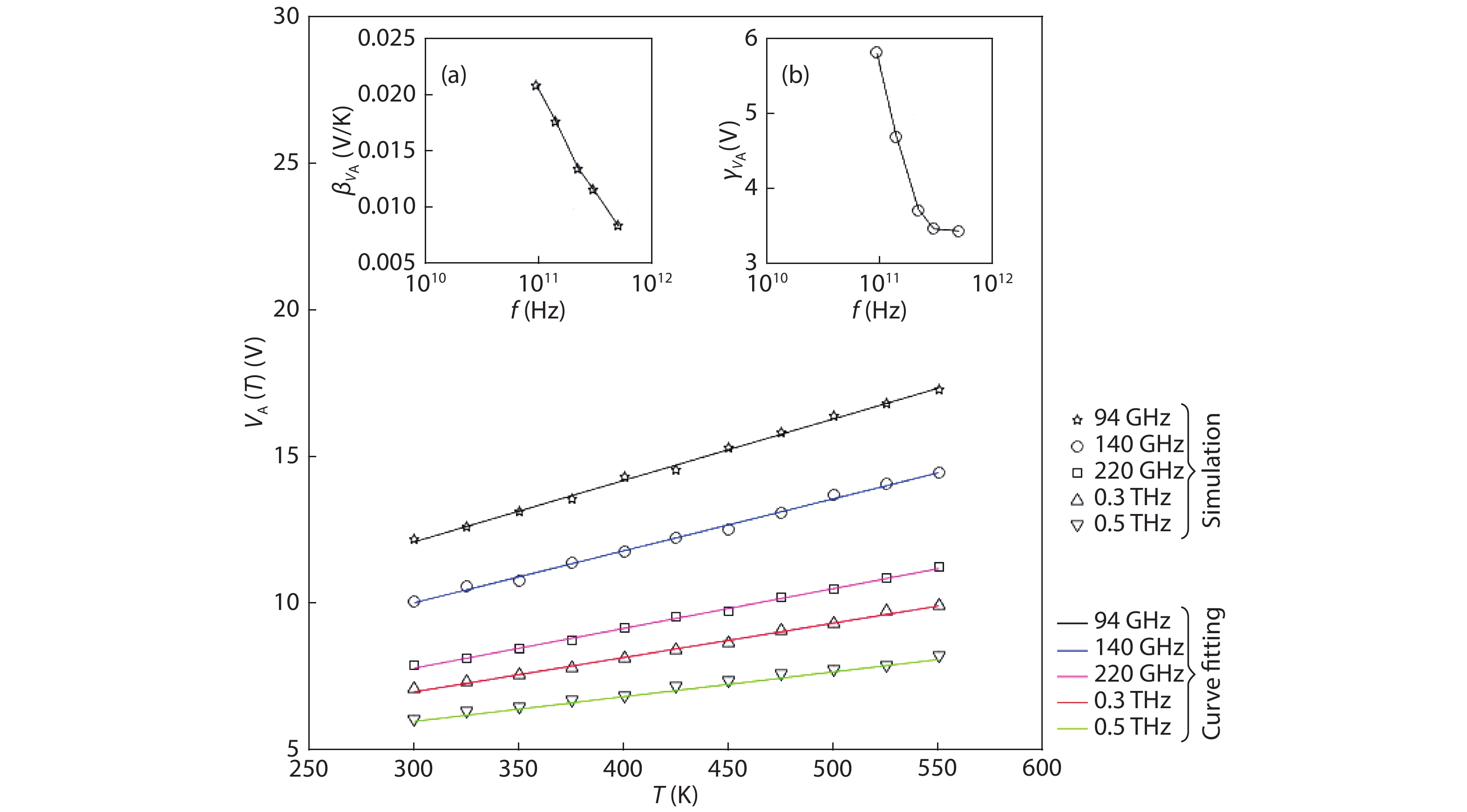
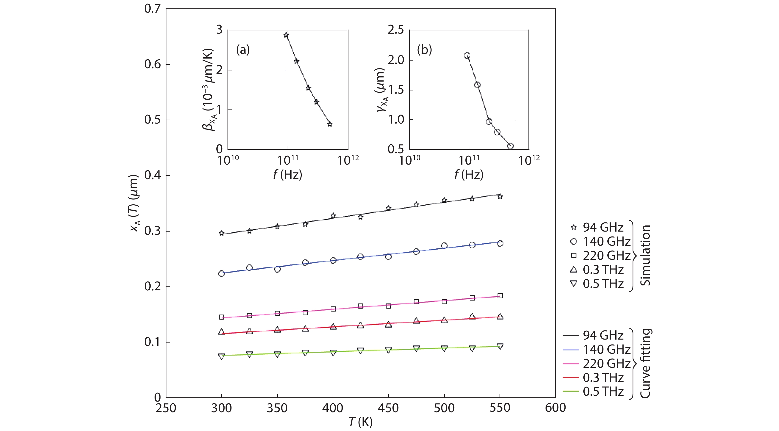
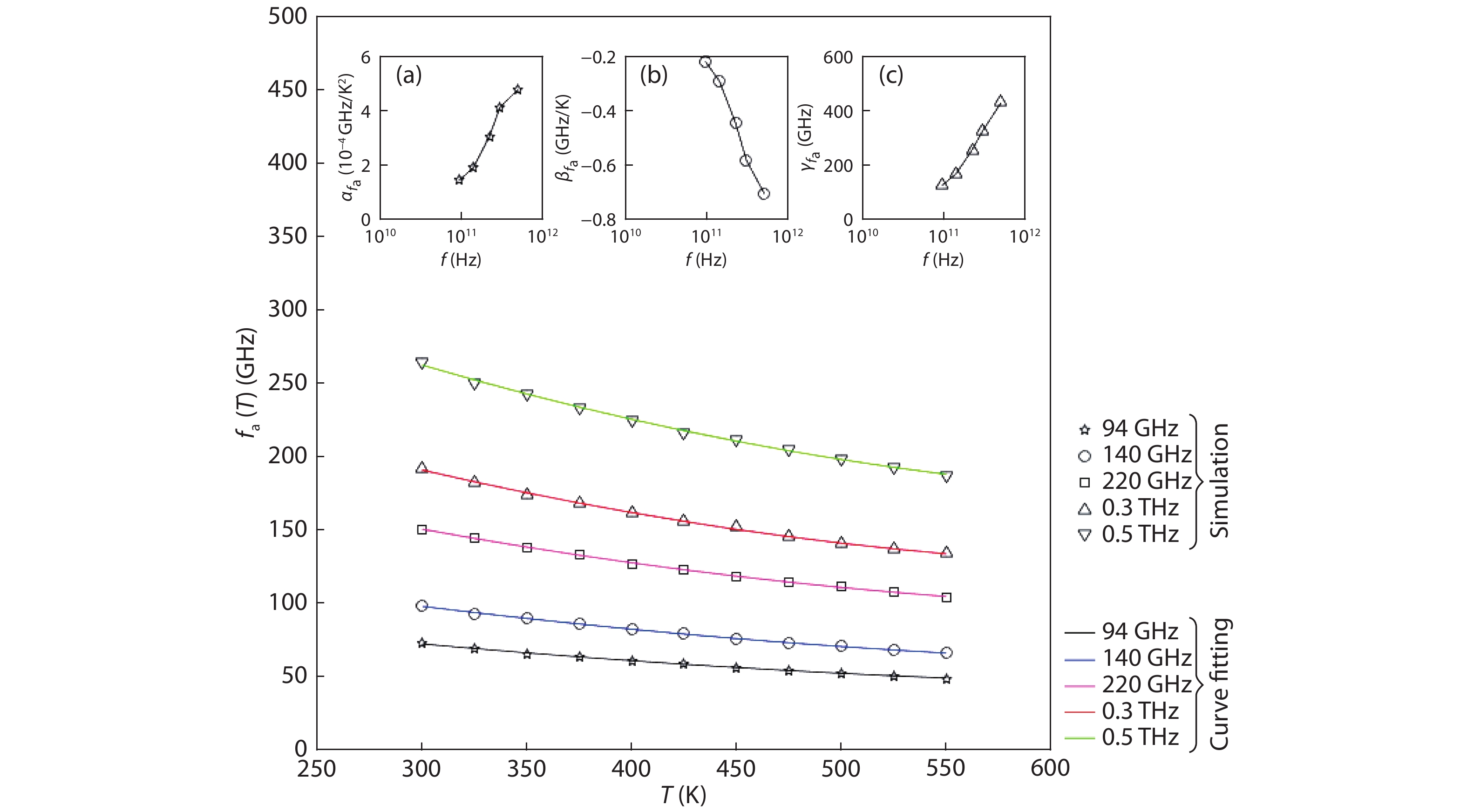
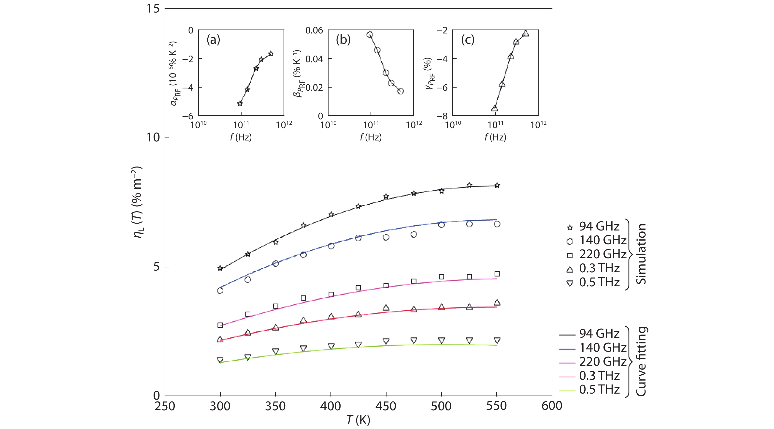
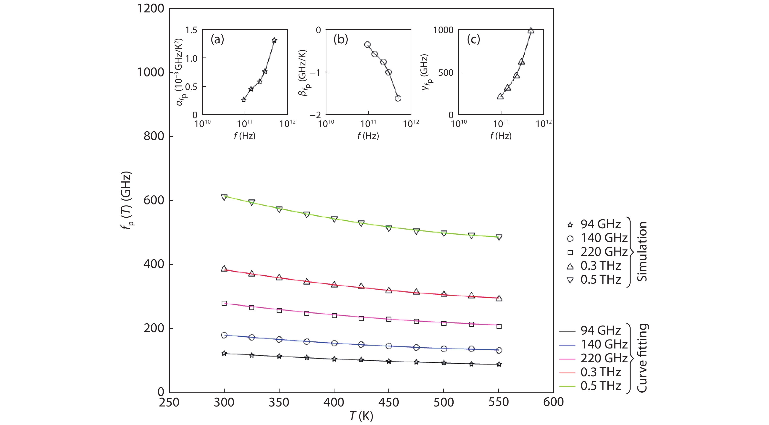
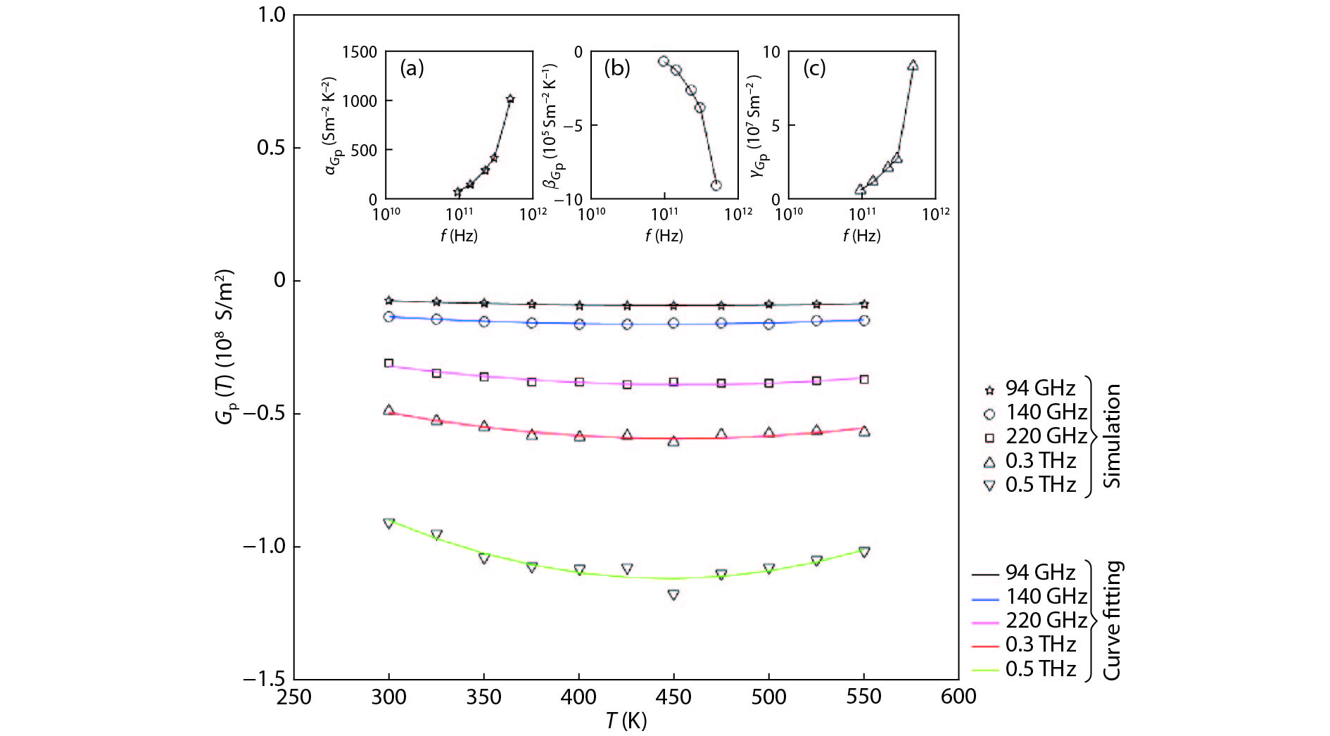
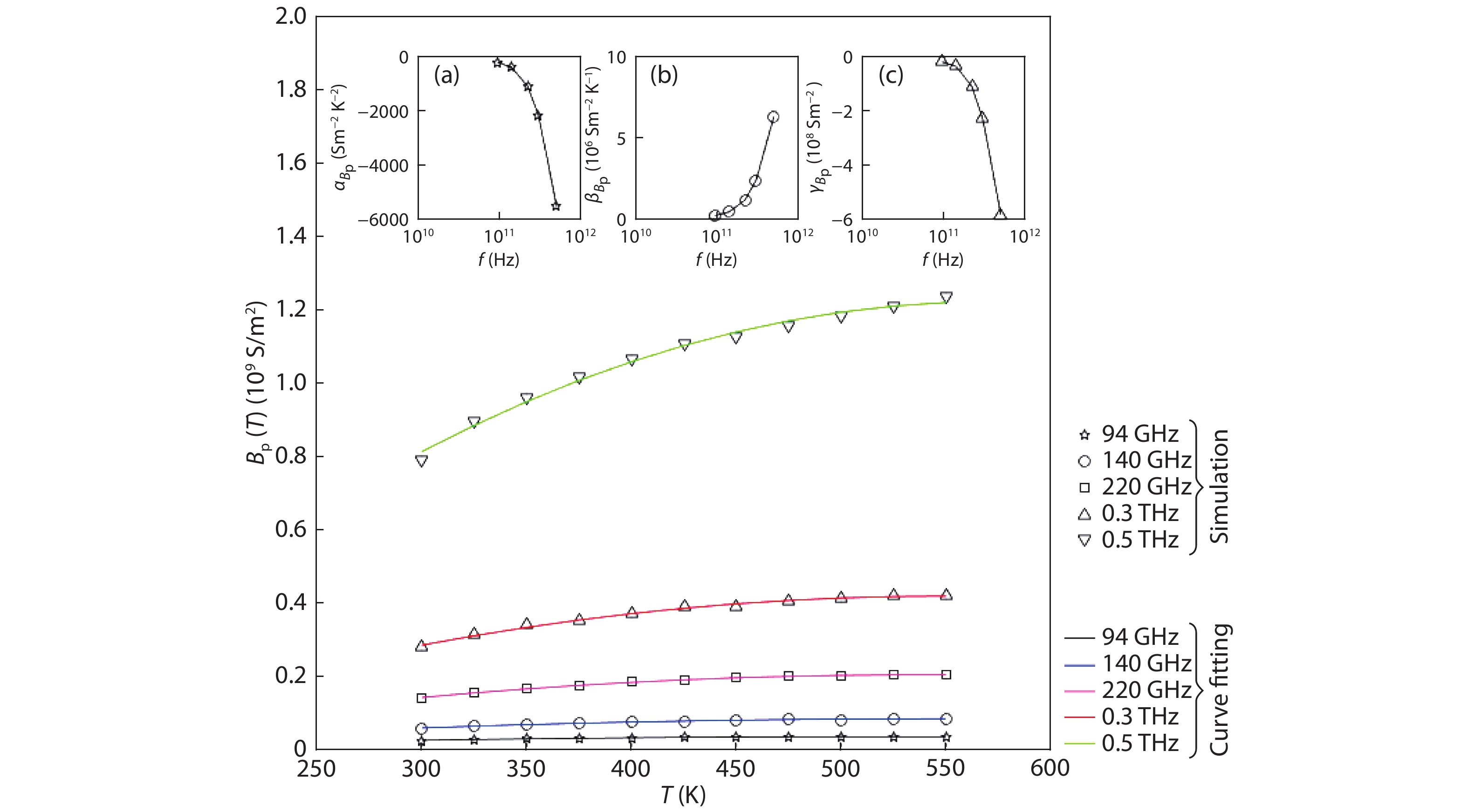
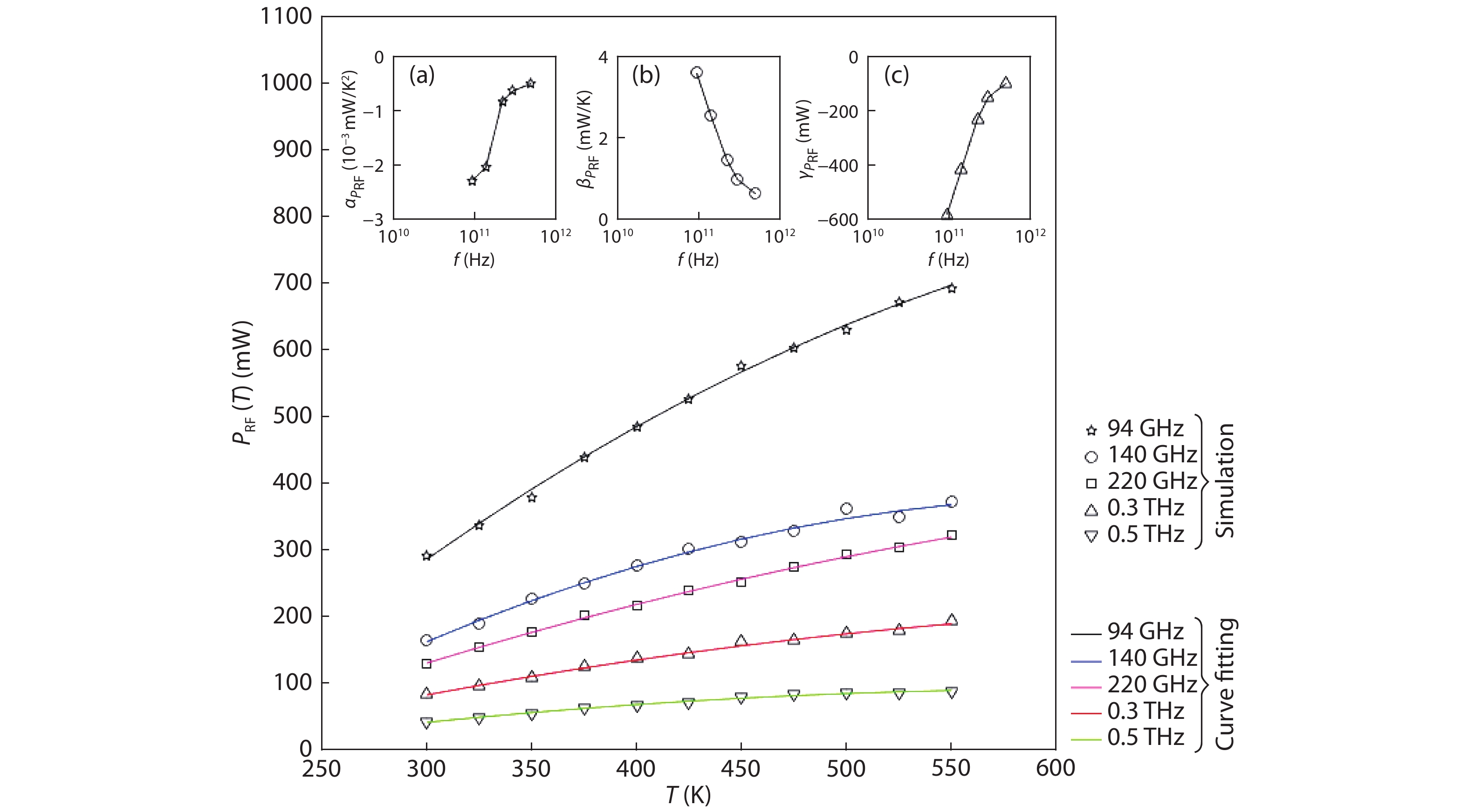
The influence of self-heating on the millimeter-wave (mm-wave) and terahertz (THz) performance of double-drift region (DDR) impact avalanche transit time (IMPATT) sources based on silicon (Si) has been investigated in this paper. The dependences of static and large-signal parameters on junction temperature are estimated using a non-sinusoidal voltage excited (NSVE) large-signal simulation technique developed by the authors, which is based on the quantum-corrected drift-diffusion (QCDD) model. Linear variations of static parameters and non-linear variations of large-signal parameters with temperature have been observed. Analytical expressions representing the temperature dependences of static and large-signal parameters of the diodes are developed using linear and 2nd degree polynomial curve fitting techniques, which will be highly useful for optimizing the thermal design of the oscillators. Finally, the simulated results are found to be in close agreement with the experimentally measured data. -
References
[1] Acharyya A. Three-terminal graphene nanoribbon tunable avalanche transit time sources for terahertz power generation. Phys Status Solidi A, 2019, 216, 1900277 doi: 10.1002/pssa.201900277[2] Acharyya A. 1.0–10.0 THz radiation from graphene nanoribbon based avalanche transit time sources. Phys Status Solidi A, 2019, 216, 1800730 doi: 10.1002/pssa.201800730[3] Biswas A, Sinha S, Acharyya A, et al. 1.0 THz GaN IMPATT source: effect of parasitic series resistance. J Infrared, Millimeter Terahertz Waves, 2018, 39(10), 954 doi: 10.1007/s10762-018-0509-z[4] Acharyya A. Gallium phosphide IMPATT sources for millimeter-wave applications. Iran J Electr Electron Eng, 2018, 14(2), 143 doi: 10.22068/IJEEE.14.2.143[5] Midford T A, Bernick R L. Millimeter Wave CW IMPATT diodes and oscillators. IEEE Trans Microwave Theory Tech, 1979, 27, 483 doi: 10.1109/TMTT.1979.1129653[6] Chang Y, Hellum J M, Paul J A, et al. Millimeter-wave IMPATT sources for communication applications. IEEE MTT-S International Microwave Symposium Digest, 1977, 1, 216[7] Gray W W, Kikushima L, Morentc N P, et al. Applying IMPATT power sources to modern microwave systems. IEEE J Solid-State Circuits, 1969, 4, 409 doi: 10.1109/JSSC.1969.1050046[8] Acharyya A, Banerjee J P. Prospects of IMPATT devices based on wide bandgap semiconductors as potential terahertz sources. Appl Nanosci, 2014, 4, 1 doi: 10.1007/s13204-012-0172-y[9] Eisele H. Selective etching technology for 94 GHz, GaAs IMPATT diodes on diamond heat sinks. Solid State Electron, 1989, 32(3), 253 doi: 10.1016/0038-1101(89)90100-7[10] Tschernitz M, Freyer J. 140 GHz GaAs double-read IMPATT diodes. Electron Lett, 1995, 31(7), 582 doi: 10.1049/el:19950390[11] Berenz J J, Fank F B, Hierl T L. Ion-implanted p–n junction indium-phosphide IMPATT diodes. Electron Lett, 1978, 14(21), 683 doi: 10.1049/el:19780461[12] Yuan L, James A, Cooper J A, et al. Experimental demonstration of a silicon carbide IMPATT oscillator. IEEE Electron Device Lett, 2001, 22, 266 doi: 10.1109/55.924837[13] Vassilevski K V, Zorenko A V, Zekentes K, et al. 4H-SiC IMPATT diode fabrication and testing. Technical Digest of International Conference on SiC and Related Materials, 2001, 713 doi: 10.4028/www.scientific.net/msf.389-393.1353[14] Mock P M, Trew R J. RF performance characteristics of double-drift MM-wave diamond IMPATT diodes. Proc of IEEE/Cornell Conf Advanced Concepts in High-Speed Semiconductor Devices and Circuits, 1989, 383[15] Banerjee S, Acharyya A, Banerjee J P. Noise performance of heterojunction DDR MITATT devices based on Si~Si1– xGex at W-band. Active and Passive Electronic Components, 2013, 2013, 1 doi: 10.1155/2013/720191[16] Banerjee S, Acharyya A, Banerjee J P, et al. Large-signal and noise properties of heterojunction DDR IMPATTs basd on AlxGa1–xN~GaN material system at 1.0 THz. Proceedings of 2nd International Conference on Foundations and Frontiers in Communication, Computer and Electrical Engineering (C2E2 – 2015), 2015[17] Banerjee S, Acharyya A, Mitra M, et al. Large-signal properties of 3C-SiC/Si heterojunction DDR IMPATT devices at terahertz frequencies. Proceedings of the 34th PIERS, 2013, 462[18] Luy J F, Casel A, Behr W, et al. A 90-GHz double-drift IMPATT diode made with Si MBE. IEEE Trans Electron Devices, 1987, 34, 1084 doi: 10.1109/T-ED.1987.23049[19] Dalle C, Rolland P, Lieti G. Flat doping profile double-drift silicon IMPATT for reliable CW high power high-efficiency generation in the 94-GHz window. IEEE Trans Electron Devices, 1990, 37, 227 doi: 10.1109/16.43820[20] Wollitzer M, Buchler J, Schafflr F, et al. D-band Si-IMPATT diodes with 300 mW CW output power at 140 GHz. Electron Lett, 1996, 32, 122 doi: 10.1049/el:19960088[21] Acharyya A, Chakraborty J, Das K, et al. Large-signal characterization of DDR silicon IMPATTs operating up to 0.5 THz. Int J Microwave Wireless Technol, 2013, 5, 567 doi: 10.1017/S1759078713000597[22] Acharyya A, Banerjee S, Banerjee J P. Effect of junction temperature on the large-signal properties of a 94 GHz silicon based double-drift region impact avalanche transit time device. J Semicond, 2013, 34, 024001 doi: 10.1088/1674-4926/34/2/024001[23] Acharyya A, Goswami J, Banerjee S, et al. Quantum corrected drift-diffusion model for terahertz IMPATTs based on different semiconductors. J Comput Electron, 2015, 14, 309 doi: 10.1007/s10825-014-0658-9[24] Sze S M, Ryder R M. Microwave avalanche diodes. Proc IEEE, 1971, 59, 1140 doi: 10.1109/PROC.1971.8360[25] Grant W N. Electron and hole ionization rates in epitaxial silicon at high electric fields. Solid State Electron, 1973, 16, 1189 doi: 10.1016/0038-1101(73)90147-0[26] Canali C, Ottaviani G, Quaranta A A. Drift velocity of electrons and holes and associated anisotropic effects in silicon. J Phys Chem Solids, 1971, 32, 1707 doi: 10.1016/S0022-3697(71)80137-3[27] Electronic archive: new semiconductor materials, characteristics and properties. Available from: http://www.ioffe.ru/SVA/NSM/Semicond/index.html (Last accessed on: July 2019)[28] Zeghbroeck B V. Principles of semiconductor devices. Colorado Press, 2011[29] Varshini Y P. Temperature dependence of the energy gap in semiconductors. Physica, 1967, 34, 149 doi: 10.1016/0031-8914(67)90062-6[30] Kern W, Puotinen D A. Cleaning solutions based on hydrogen peroxide for use in silicon semiconductor technology. RCA Rev, 1970, 31, 187[31] Kugimiya K, Hirofuji Y, Matsuo N. Si-beam radiation cleaning in molecular-beam epitaxy. Jpn J Appl Phys, 1985, 24(5), 564 doi: 10.1143/jjap.24.564[32] Jorke H, Kibbel H. Doping by secondary implantation. J Electrochem Soc, 1986, 133, 774 doi: 10.1149/1.2108674[33] Iyer S S, Metzger R A, Allen F G. Sharp profiles with high and low doping levels in silicon growth by molecular beam epitaxy. J Appl Phys, 1981, 52(2), 5608 doi: 10.1063/1.329494[34] Koenig U, Herzog H J, Jorke H, et al. Si-MBE with a high throughput of large diameter wafers. 2nd Int Symp MBE and Related Clean Surface Techniques (Tokyo), 1982, 193[35] Casel A, Jorke H, Kasper E, et al. Dependence of hole transport on Ga doping in Si molecular beam epitaxial layers. Appl Phys Lett, 1986, 48, 922 doi: 10.1063/1.96659[36] Acharyya A, Chatterjee S, Goswami J, et al. Quantum drift-diffusion model for IMPATT devices. J Comput Electron, 2014, 13, 739 doi: 10.1007/s10825-014-0595-7[37] Acharyya A, Mukherjee M, Banerjee J P. Effects of tunnelling current on mm-wave IMPATT devices. Int J Electron, 2015, 102(9), 1429 doi: 10.1080/00207217.2014.982211[38] Acharyya A, Ghosh S. Dark current reduction in nano-avalanche photodiodes by incorporating multiple quantum barriers. Int J Electron, 2017, 104(12), 1957 doi: 10.1080/00207217.2017.1330426[39] Dash G N, Pati S P. Small-signal computer simulation of IMPATT diodes including carrier diffusion. Semicond Sci Technol, 1991, 6, 348 doi: 10.1088/0268-1242/6/5/006[40] Acharyya A, Banerjee S, Banerjee J P. Influence of skin effect on the series resistance of millimeter-wave of IMPATT devices. J Comput Electron, 2013, 12, 511 doi: 10.1007/s10825-013-0470-y[41] Acharyya A, Banerjee S, Banerjee J P. A proposed simulation technique to study the series resistance and related millimeter-wave properties of Ka-band Si IMPATTs from the electric field snap-shots. Int J Microwave Wireless Technol, 2013, 5(1), 91 doi: 10.1017/S1759078712000839[42] Bandyopadhyay A M, Acharyya A, Banerjee J P. Multiple-band large-signal characterization of millimeter-wave double avalanche region transit time diode. J Comput Electron, 2014, 13, 769 doi: 10.1007/s10825-014-0599-3 -
Proportional views


 DownLoad:
