| [1] |
Henini M. Molecular beam epitaxy: from research to mass production. Elsevier, 2012
|
| [2] |
Wang G, Liu B L, Balocchi A, et al. Gate control of the electron spin-diffusion length in semiconductor quantum wells. Nat Commun, 2013, 4, 2372 doi: 10.1038/ncomms3372 |
| [3] |
Zhou X Y, Uppu R, Liu Z, et al. On-chip nanomechanical filtering of quantum-dot single-photon sources. Laser Photonics Rev, 2020, 14, 1900404 doi: 10.1002/lpor.201900404 |
| [4] |
Ghali M, Ohtani K, Ohno Y, et al. Generation and control of polarization-entangled photons from GaAs Island quantum dots by an electric field. Nat Commun, 2012, 3, 661 doi: 10.1038/ncomms1657 |
| [5] |
Schliemann J. Colloquium: Persistent spin textures in semiconductor nanostructures. Rev Mod Phys, 2017, 89, 011001 doi: 10.1103/RevModPhys.89.011001 |
| [6] |
Poltavtsev S V, Yugova I A, Kosarev A N, et al. In-plane anisotropy of the hole g factor in CdTe/(Cd, Mg)Te quantum wells studied by spin-dependent photon echoes. Phys Rev Res, 2020, 2, 023160 doi: 10.1103/PhysRevResearch.2.023160 |
| [7] |
Klenovský P, Baranowski P, Wojnar P. Excitonic fine structure of epitaxial Cd(Se, Te) on ZnTe type-II quantum dots. Phys Rev B, 2022, 105, 195403 doi: 10.1103/PhysRevB.105.195403 |
| [8] |
Zhukov E A, Yakovlev D R, Glazov M M, et al. Optical control of electron spin coherence in CdTe/(Cd, Mg)Te quantum wells. Phys Rev B, 2010, 81, 235320 doi: 10.1103/PhysRevB.81.235320 |
| [9] |
Ghali M, Kossut J, Heiss W. Spin injection through different g-factor heterointerfaces using negative trions for spin detection. Appl Phys Lett, 2003, 82, 541 doi: 10.1063/1.1540219 |
| [10] |
Zhukov E A, Yakovlev D R, Gerbracht M, et al. Spin coherence of holes and electrons in undoped CdTe/(Cd, Mg)Te quantum wells. Phys Rev B, 2009, 79, 155318 doi: 10.1103/PhysRevB.79.155318 |
| [11] |
Mohanta M K, Is F, Kishore A, et al. Spin-current modulation in hexagonal buckled ZnTe and CdTe monolayers for self-powered flexible-piezo-spintronic devices. ACS Appl Mater Interfaces, 2021, 13, 40872 doi: 10.1021/acsami.1c09267 |
| [12] |
Lei W, Gu R J, Antoszewski J, et al. GaSb: A new alternative substrate for epitaxial growth of HgCdTe. J Electron Mater, 2014, 43, 2788 doi: 10.1007/s11664-014-3049-x |
| [13] |
Lei W, Antoszewski J, Faraone L. Progress, challenges, and opportunities for HgCdTe infrared materials and detectors. Appl Phys Rev, 2015, 2, 041303 doi: 10.1063/1.4936577 |
| [14] |
Varavin V S, Dvoretskii S A, Mikhailov N N, et al. Molecular beam epitaxy of CdHgTe: Current state and horizons. Optoelectron Instrum Data Process, 2020, 56, 456 doi: 10.3103/S8756699020050143 |
| [15] |
Passmann F, Anghel S, Tischler T, et al. Persistent spin helix manipulation by optical doping of a CdTe quantum well. Phys Rev B, 2018, 97, 201413 doi: 10.1103/PhysRevB.97.201413 |
| [16] |
Su P Y, Lee C, Wang G C, et al. CdTe/ZnTe/GaAs heterostructures for single-crystal CdTe solar cells. J Electron Mater, 2014, 43, 2895 doi: 10.1007/s11664-014-3142-1 |
| [17] |
Alshahrani B, Nabil S, Elsaeedy H I, et al. The pivotal role of thermal annealing of cadmium telluride thin film in optimizing the performance of CdTe/Si solar cells. J Electron Mater, 2021, 50, 4586 doi: 10.1007/s11664-021-08989-3 |
| [18] |
Suela J, Ribeiro I R B, Ferreira S O, et al. Evolution of crystalline domain size and epitaxial orientation of CdTe/Si(111) quantum dots. J Appl Phys, 2010, 107, 064305 doi: 10.1063/1.3357292 |
| [19] |
Chaudhari B S, Goto H, Niraula M, et al. Analysis of dislocations and their correlation with dark currents in CdTe/Si heterojunction diode-type X-ray detectors. J Appl Phys, 2021, 130, 055302 doi: 10.1063/5.0058504 |
| [20] |
Zhang Q, Li Y P, Pagliero D, et al. Controlled growth of (100) or (111) CdTe epitaxial layers on (100) GaAs by molecular beam epitaxy and study of their electron spin relaxation times. J Vac Sci Technol B, 2010, 28, C3D1 doi: 10.1116/1.3336144 |
| [21] |
Zhao J, Zeng Y P, Liu C, et al. Effects of a ZnTe buffer layer on structural quality and morphology of CdTe epilayer grown on (001) GaAs by molecular beam epitaxy. Vacuum, 2012, 86, 1062 doi: 10.1016/j.vacuum.2011.05.008 |
| [22] |
Zhu X L, Wu J Q, Hu Q M, et al. Improved growth quality of epitaxial ZnTe thin films on Si (111) wafer with ZnSe buffer layer. J Vac Sci Technol A Vac Surf Films, 2021, 39, 063410 doi: 10.1116/6.0001257 |
| [23] |
Park K D, Man M T, Cho D Y, et al. Wide-gap photoluminescence control of quantum dots through atomic interdiffusion and bandgap renormalization. Nanophotonics, 2020, 9, 4799 doi: 10.1515/nanoph-2020-0482 |
| [24] |
Ghosh S, Rodrigues L N, Moura L G, et al. Epitaxial growth and characterization of Cd 1–xMn xTe films on Si(1 1 1) substrates. J Cryst Growth, 2019, 522, 25 doi: 10.1016/j.jcrysgro.2019.06.009 |
| [25] |
Oliveira J M, Malachias A, Ospina C A, et al. Nondestructive monitoring of defect evolution in epitaxial CdTe thin layers grown on Si(111). J Phys Chem C, 2014, 118, 1968 doi: 10.1021/jp409538p |
| [26] |
Ferreira S O, Paiva E C, Fontes G N, et al. Characterization of CdTe quantum dots grown on Si(111) by hot wall epitaxy. J Appl Phys, 2003, 93, 1195 doi: 10.1063/1.1530364 |
| [27] |
Sakaki H, Noda T, Hirakawa K, et al. Interface roughness scattering in GaAs/AlAs quantum wells. Appl Phys Lett, 1987, 51, 1934 doi: 10.1063/1.98305 |
| [28] |
Yamakawa I, Oga R, Fujiwara Y, et al. Atomic-scale observation of interfacial roughness and As–P exchange in InGaAs/InP multiple quantum wells. Appl Phys Lett, 2004, 84, 4436 doi: 10.1063/1.1758784 |
| [29] |
Blanks D K, Bicknell R N, Giles-Taylor N C, et al. Strain effects in Cd 1–xMn xTe–CdTe superlattices. J Vac Sci Technol A Vac Surf Films, 1986, 4, 2120 doi: 10.1116/1.574040 |
| [30] |
Nurmikko A V, Hefetz Y, Chang S K, et al. Influence of heterointerfaces on optical properties of CdTe/(Cd, Mn)Te and ZnSe/(Zn, Mn)Se superlattices. J Vac Sci Technol B Microelectron Process Phenom, 1986, 4, 1033 doi: 10.1116/1.583575 |
| [31] |
Giles-Taylor N C, Bicknell R N, Blanks D K, et al. Photoluminescence of CdTe: A comparison of bulk and epitaxial material. J Vac Sci Technol A Vac Surf Films, 1985, 3, 76 doi: 10.1116/1.573250 |
| [32] |
Davis C B, Allred D D, Reyes-Mena A, et al. Photoluminescence and absorption studies of defects in CdTe and Zn xCd 1-xTe crystals. Phys Rev B Condens Matter, 1993, 47, 13363 doi: 10.1103/PhysRevB.47.13363 |
| [33] |
Halliday D P, Potter M D G, Mullins J T, et al. Photoluminescence study of a bulk vapour grown CdTe crystal. J Cryst Growth, 2000, 220, 30 doi: 10.1016/S0022-0248(00)00755-7 |
| [34] |
Xu Z Y, Xu J Z, Ge W K, et al. The excitonic properties and temperature behaviour of the photoluminescence from GaAs-GaAlAs multiple quantum well structures. Solid State Commun, 1987, 61, 707 doi: 10.1016/0038-1098(87)90721-6 |
| [35] |
Adachi S. Handbook on physical properties of semiconductors. Springer Science & Business Media, 2004
|
| [36] |
Zhukov A E, Ustinov V M, Egorov A Y, et al. Negative characteristic temperature of InGaAs quantum dot injection laser. Jpn J Appl Phys, 1997, 36, 4216 doi: 10.1143/JJAP.36.4216 |
| [37] |
Karczewski G, Maćkowski S, Kutrowski M, et al. Photoluminescence study of CdTe/ZnTe self-assembled quantum dots. Appl Phys Lett, 1999, 74, 3011 doi: 10.1063/1.123996 |
| [38] |
Godlewski M, Narkowicz R, Wojtowicz T, et al. Quasi-zero-dimensional excitons in quantum well structures of CdTe/CdMnTe. J Cryst Growth, 2000, 214/215, 420 doi: 10.1016/S0022-0248(00)00121-4 |
| [39] |
Lourenço S A, Dias I F L, Duarte J L, et al. Temperature-dependent photoluminescence spectra of GaAsSb/AlGaAs and GaAsSbN/GaAs single quantum wells under different excitation intensities. Braz J Phys, 2007, 37, 1212 doi: 10.1590/S0103-97332007000800004 |
| [40] |
Mazur Y I, Dorogan V G, Benamara M, et al. Effects of spatial confinement and layer disorder in photoluminescence of GaAs 1–xBi x/GaAs heterostructures. J Phys D: Appl Phys, 2013, 46, 065306 doi: 10.1088/0022-3727/46/6/065306 |
| [41] |
Kłopotowski, Nawrocki M, Gaj J A, et al. Tunneling of spin polarized excitons in CdTe based asymmetric double quantum well structure. Solid State Commun, 2001, 119, 147 doi: 10.1016/S0038-1098(01)00230-7 |
| [42] |
Besombes L, Kheng K, Martrou D. Exciton and biexciton fine structure in single elongated islands grown on a vicinal surface. Phys Rev Lett, 2000, 85, 425 doi: 10.1103/PhysRevLett.85.425 |
| [43] |
Wei Y M, Zhao T M, Yao B M, et al. Bright and highly-polarized single-photon sources in visible based on droplet-epitaxial GaAs quantum dots in photonic crystal cavities. Opt Mater Express, 2019, 10, 170 doi: 10.1364/OME.379424 |
| [44] |
Lodahl P, Mahmoodian S, Stobbe S. Interfacing single photons and single quantum dots with photonic nanostructures. Rev Mod Phys, 2015, 87, 347 doi: 10.1103/RevModPhys.87.347 |
| [45] |
Arakawa Y, Holmes M J. Progress in quantum-dot single photon sources for quantum information technologies: A broad spectrum overview. Appl Phys Rev, 2020, 7, 021309 doi: 10.1063/5.0010193 |
| [46] |
Zhang J X, Wildmann J S, Ding F, et al. High yield and ultrafast sources of electrically triggered entangled-photon pairs based on strain-tunable quantum dots. Nat Commun, 2015, 6, 10067 doi: 10.1038/ncomms10067 |


 Leonarde N. Rodrigues Leonarde do Nascimento Rodrigues received his doctoral degree from Federal University of Juiz de Fora, Juiz de Fora, Brazil, in 2016. He is currently a Professor in the Physics Department at the Federal University of Viçosa, Brazil. His main research area is the epitaxial growth of semiconductor heterostructures and thin flms, fabrication of semiconductor nanomembranes and devices and their characterizalion by high resolution X-ray diffraction and optical spectroscopy as inelastic light scattering and photoluminescence.
 Wesley F. Inoch Wesley Fiorio lnoch received his undergraduate degree from Federal University of Viçosa, Brazil, in 2021. He is curently a PhD student at Physics Department at the Federal Universily of Viçosa, Brazil. His main research area is the epitaxial growth of semiconductor heterostructures and thin flms, fabrication of structures using nanolithography, and their characterization by high resolution X-ray diffraction clectron microscopy and scanning probe microscopy.
 Bráulio S. Archanjo Braulio Archanjo got his PhD in Physics from the Federal University of Minas Gerais andcompleted a post-doc at the National Center for Electron Microscopy (NCEM) at Lawrence Berkeley National Laboratory. Currently serves as a Researcher at INMETRO's Materials Me trology Division, acting as head of the Microscopy Laboratories. Experienced in materials science, specializing in nanoscience, nanotechnology, and nanomctrology. Proficient in transmission electron microscopy, scanning electron microscopy, focused ion beam (FlB), helium ion beam microscopy, X-ray diffraction, micro-Raman spectroscopy, scanning probe microscopy, photoelectron spectroscopy, chemical vapor deposition (CVD), self-assembly, microfabrication and two-dimensional materials.
 Sukarno O. Ferreira Sukarno Olavo Ferreira received his doctoral degree from Johannes Kepler Universitat, Linz, Austria, in 1995. He is currently a Professor in the Physics Department at the Federal University of Viçosa, Brazil. His main research area is the epitaxial growth of Ⅱ−Ⅵ semiconductor heterostructures and thin flms and their characterization by clectron microscopy, scanning probe microscopy and high resolution X-ray diffraction.
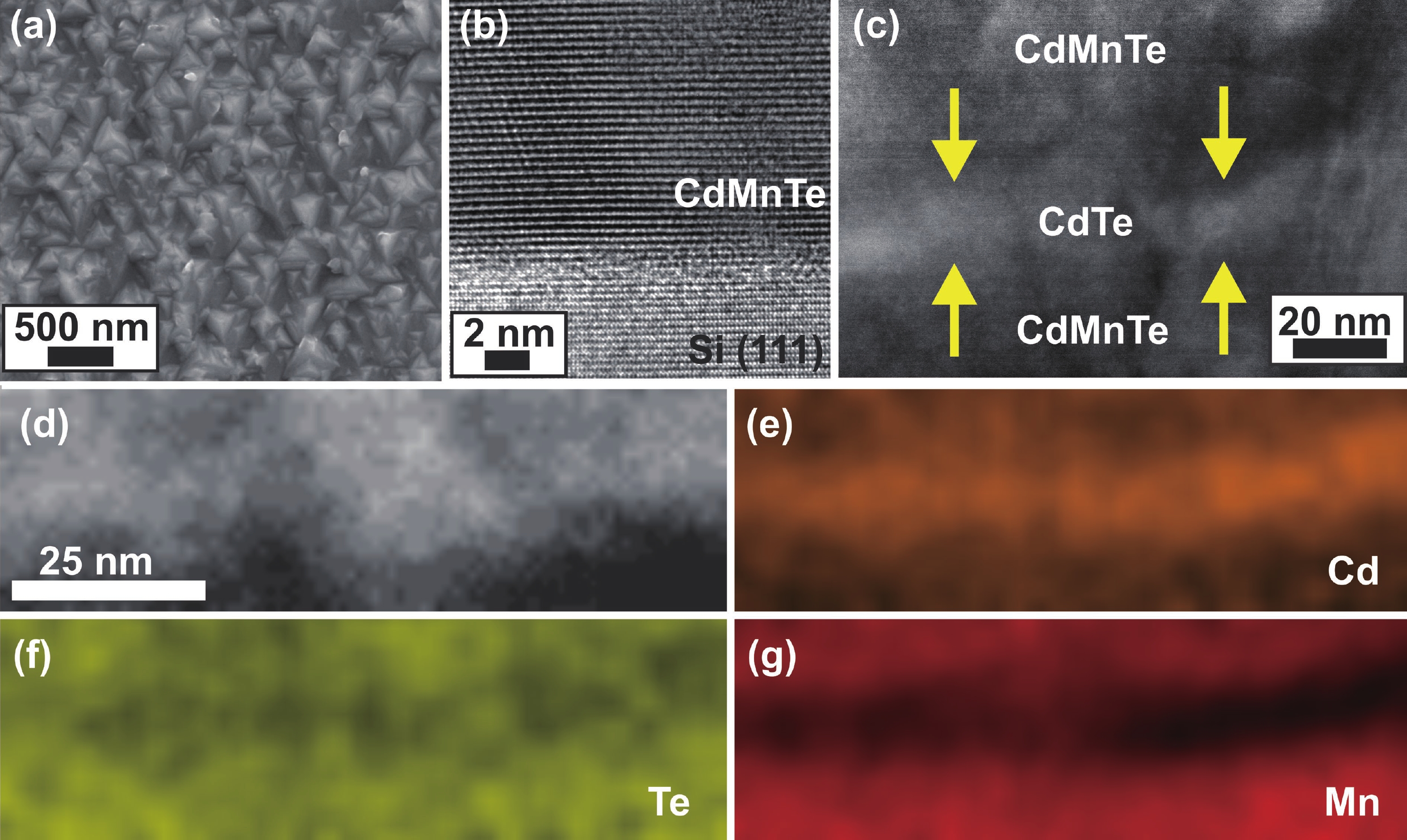
 DownLoad: