| Citation: |
Xiyu Hou, Lianjun Wen, Fengyue He, Ran Zhuo, Lei Liu, Hailong Wang, Qing Zhong, Dong Pan, Jianhua Zhao. Embedded high-quality ternary GaAs1−xSbx quantum dots in GaAs nanowires by molecular-beam epitaxy[J]. Journal of Semiconductors, 2024, 45(8): 082101. doi: 10.1088/1674-4926/24030038
****
X Y Hou, L J Wen, F Y He, R Zhuo, L Liu, H L Wang, Q Zhong, D Pan, and J H Zhao, Embedded high-quality ternary GaAs1−xSbx quantum dots in GaAs nanowires by molecular-beam epitaxy[J]. J. Semicond., 2024, 45(8), 082101 doi: 10.1088/1674-4926/24030038
|
Embedded high-quality ternary GaAs1−xSbx quantum dots in GaAs nanowires by molecular-beam epitaxy
DOI: 10.1088/1674-4926/24030038
More Information
-
Abstract
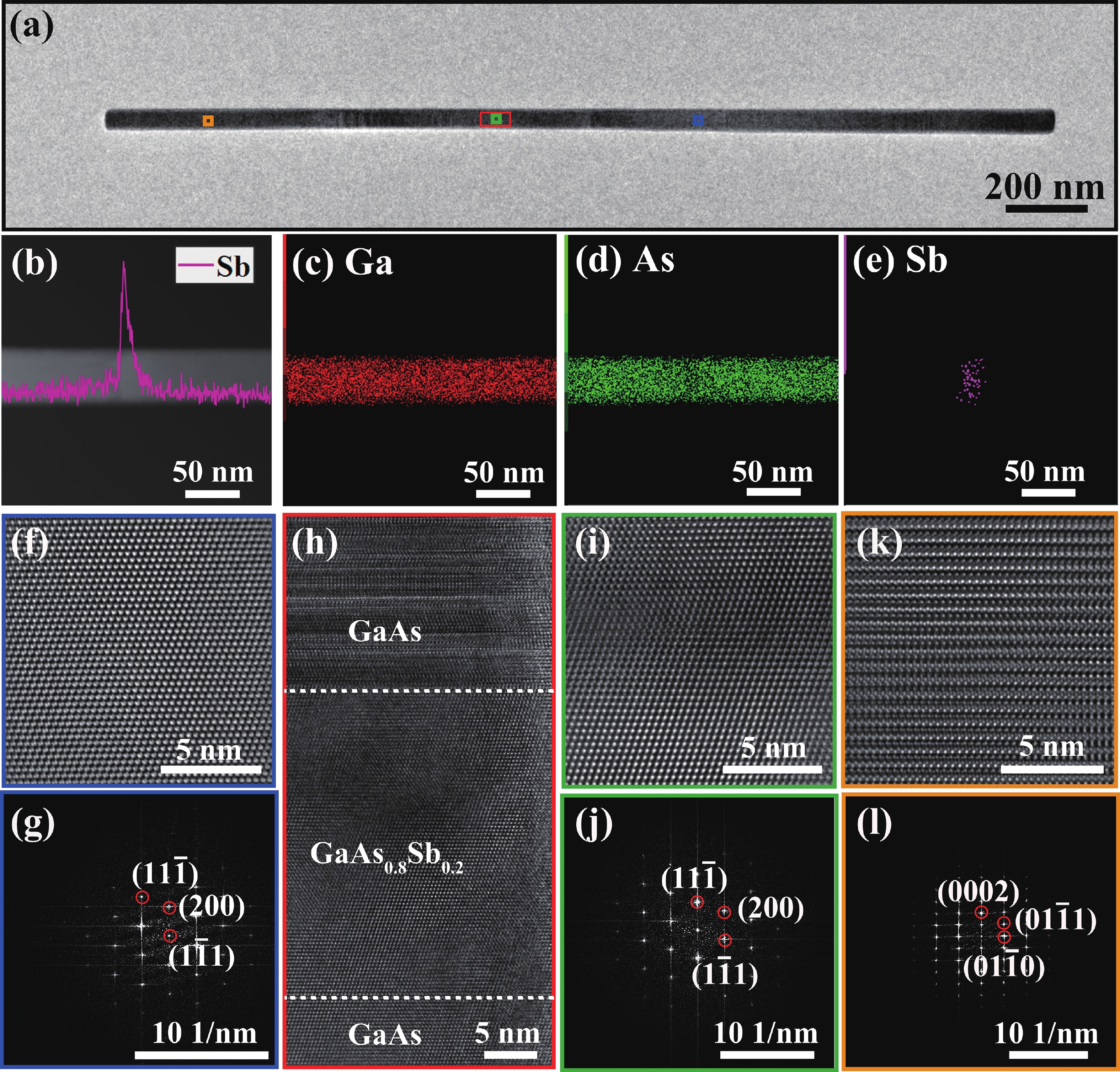
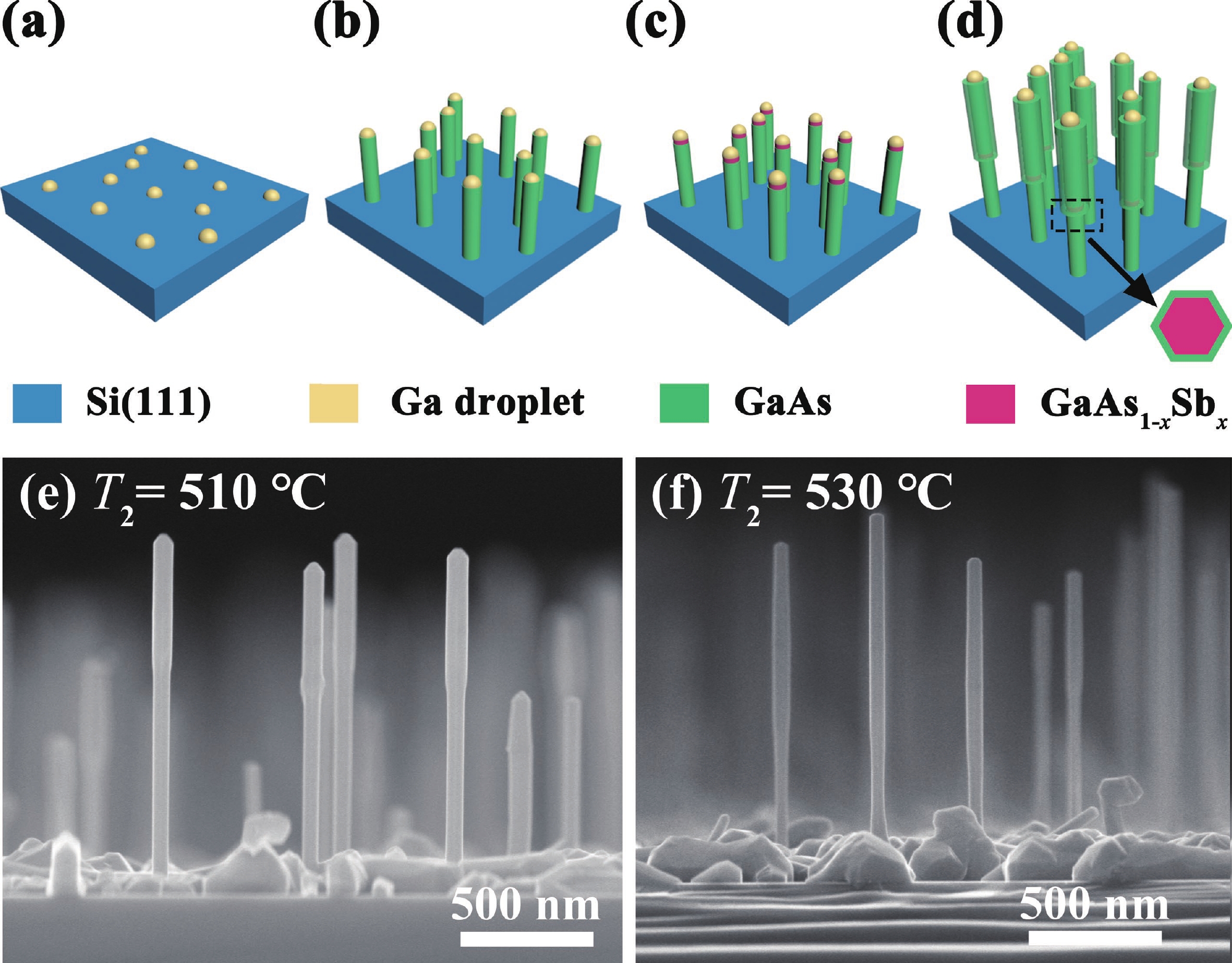
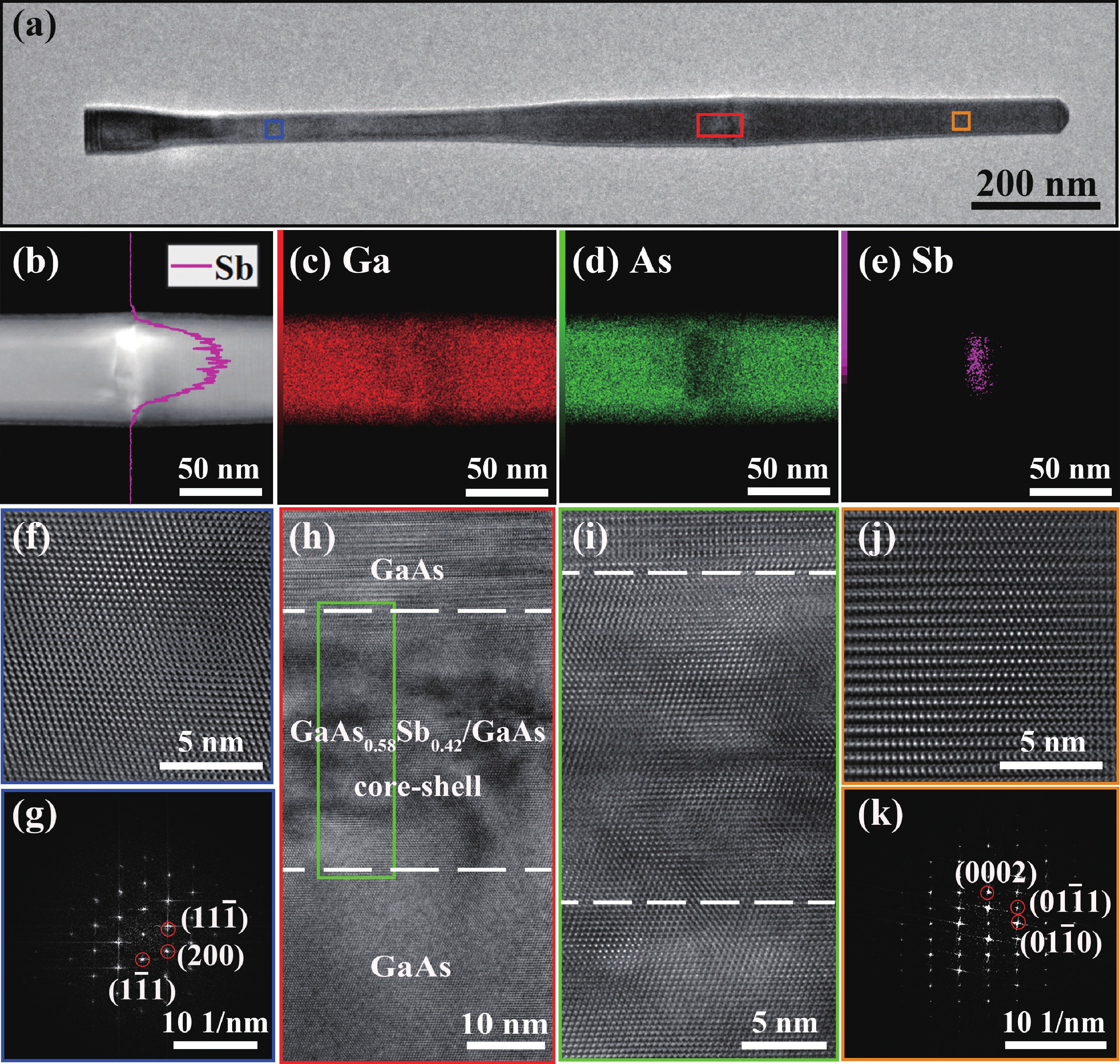
Semiconductor quantum dots are promising candidates for preparing high-performance single photon sources. A basic requirement for this application is realizing the controlled growth of high-quality semiconductor quantum dots. Here, we report the growth of embedded GaAs1−xSbx quantum dots in GaAs nanowires by molecular-beam epitaxy. It is found that the size of the GaAs1−xSbx quantum dot can be well-defined by the GaAs nanowire. Energy dispersive spectroscopy analyses show that the antimony content x can be up to 0.36 by tuning the growth temperature. All GaAs1−xSbx quantum dots exhibit a pure zinc-blende phase. In addition, we have developed a new technology to grow GaAs passivation layers on the sidewalls of the GaAs1−xSbx quantum dots. Different from the traditional growth process of the passivation layer, GaAs passivation layers can be grown simultaneously with the growth of the embedded GaAs1−xSbx quantum dots. The spontaneous GaAs passivation layer shows a pure zinc-blende phase due to the strict epitaxial relationship between the quantum dot and the passivation layer. The successful fabrication of embedded high-quality GaAs1−xSbx quantum dots lays the foundation for the realization of GaAs1−xSbx-based single photon sources.-
Keywords:
- semiconductor,
- quantum dot,
- nanowire,
- GaAs1−xSbx,
- molecular-beam epitaxy
-
References
[1] Pan J W, Chen Z B, Lu C Y, et al. Multiphoton entanglement and interferometry. Rev Mod Phys, 2012, 84(2), 777 doi: 10.1103/RevModPhys.84.777[2] Kok P, Munro W J, Nemoto K, et al. Linear optical quantum computing with photonic qubits. Rev Mod Phys, 2007, 79(1), 135 doi: 10.1103/RevModPhys.79.135[3] Wei Y J, He Y M, Chen M C, et al. Deterministic and robust generation of single photons from a single quantum dot with 99.5% indistinguishability using adiabatic rapid passage. Nano Lett, 2014, 14(11), 6515 doi: 10.1021/nl503081n[4] Wang H, He Y M, Chung T H, et al. Towards optimal single-photon sources from polarized microcavities. Nat Photonics, 2019, 13(11), 770 doi: 10.1038/s41566-019-0494-3[5] Li J P, Gu X M, Qin J, et al. Heralded nondestructive quantum entangling gate with single-photon sources. Phys Rev Lett, 2021, 126(14), 140501 doi: 10.1103/PhysRevLett.126.140501[6] Lu C Y, Pan J W. Quantum-dot single-photon sources for the quantum Internet. Nat Nanotechnol, 2021, 16(12), 1294 doi: 10.1038/s41565-021-01033-9[7] Pelucchi E, Fagas G, Aharonovich I, et al. The potential and global outlook of integrated photonics for quantum technologies. Nat Rev Phys, 2022, 4(3), 194 doi: 10.1038/s42254-021-00398-z[8] Proppe A H, Berkinsky D B, Zhu H, et al. Highly stable and pure single-photon emission with 250 ps optical coherence times in InP colloidal quantum dots. Nat Nanotechnol, 2023, 18(9), 993 doi: 10.1038/s41565-023-01432-0[9] Haffouz S, Zeuner K D, Dalacu D, et al. Bright single InAsP quantum dots at telecom wavelengths in position-controlled InP nanowires: The role of the photonic waveguide. Nano Lett, 2018, 18(5), 3047 doi: 10.1021/acs.nanolett.8b00550[10] Müller T, Skiba-Szymanska J, Krysa A B, et al. A quantum light-emitting diode for the standard telecom window around 1, 550 nm. Nat Commun, 2018, 9(1), 862 doi: 10.1038/s41467-018-03251-7[11] Xu S W, Wei Y M, Su R B, et al. Bright single-photon sources in the telecom band by deterministically coupling single quantum dots to a hybrid circular Bragg resonator. Photon Res, 2022, 10(8), B1 doi: 10.1364/PRJ.461034[12] Huang X Y, Su R B, Yang J W, et al. Wafer-scale epitaxial low density InAs/GaAs quantum dot for single photon emitter in three-inch substrate. Nanomaterials, 2021, 11(4), 930 doi: 10.3390/nano11040930[13] Alloing B, Zinoni C, Zwiller V, et al. Growth and characterization of single quantum dots emitting at 1300 nm. Appl Phys Lett, 2005, 86(10), 101908 doi: 10.1063/1.1872213[14] Ward M B, Karimov O Z, Unitt D C, et al. On-demand single-photon source for 1.3 μm telecom fiber. Appl Phys Lett, 2005, 86(20), 201111 doi: 10.1063/1.1922573[15] Trevisi G, Seravalli L, Frigeri P, et al. Low density InAs/(In)GaAs quantum dots emitting at long wavelengths. Nanotechnology, 2009, 20(41), 415607 doi: 10.1088/0957-4484/20/41/415607[16] Kettler J, Paul M, Olbrich F, et al. Single-photon and photon pair emission from MOVPE-grown In(Ga)As quantum dots: Shifting the emission wavelength from 1.0 to 1.3 μm. Appl Phys B, 2016, 122(48), 1 doi: 10.1007/s00340-015-6280-0[17] Olbrich F, Kettler J, Bayerbach M, et al. Temperature-dependent properties of single long-wavelength InGaAs quantum dots embedded in a strain reducing layer. J Appl Phys, 2017, 121(18), 184302 doi: 10.1063/1.4983362[18] Paul M, Kettler J, Zeuner K, et al. Metal-organic vapor-phase epitaxy-grown ultra-low density InGaAs/GaAs quantum dots exhibiting cascaded single-photon emission at 1.3 μm. Appl Phys Lett, 2015, 106(12), 122105 doi: 10.1063/1.4916349[19] Zhou X Y, Zhai L, Liu J. Epitaxial quantum dots: A semiconductor launchpad for photonic quantum technologies. Photonics Insights, 2022, 1(2), R07 doi: 10.3788/PI.2022.R07[20] Cingolani R, Rinaldi R. Optical and electrical injection of single quantum dots: Beyond the inhomogeneous broadening issues. Phys Stat Sol (b), 2002, 234(1), 411 doi: 10.1002/1521-3951(200211)234:1<411::AID-PSSB411>3.0.CO;2-A[21] Nguyen H A, Dixon G, Dou F Y, et al. Design rules for obtaining narrow luminescence from semiconductors made in solution. Chem Rev, 2023, 123(12), 7890 doi: 10.1021/acs.chemrev.3c00097[22] Perret N, Morris D, Franchomme-Fossé L, et al. Origin of the inhomogenous broadening and alloy intermixing in InAs/GaAs self-assembled quantum dots. Phys Rev B, 2000, 62(8), 5092 doi: 10.1103/PhysRevB.62.5092[23] Buckley S, Rivoire K, Vučković J. Engineered quantum dot single-photon sources. Rep Prog Phys, 2012, 75(12), 126503 doi: 10.1088/0034-4885/75/12/126503[24] Senellart P, Solomon G, White A. High-performance semiconductor quantum-dot single-photon sources. Nat Nanotechnol, 2017, 12(11), 1026 doi: 10.1038/nnano.2017.218[25] Seguin R, Schliwa A, Germann T D, et al. Control of fine-structure splitting and excitonic binding energies in selected individual InAs∕GaAs quantum dots. Appl Phys Lett, 2006, 89(26), 263109 doi: 10.1063/1.2424446[26] Kitamura S, Senshu M, Katsuyama T, et al. Optical characterization of In-flushed InAs/GaAs quantum dots emitting a broadband spectrum with multiple peaks at ~1 μm. Nanoscale Res Lett, 2015, 10(231), 1 doi: 10.1186/s11671-015-0941-0[27] Ruiz-Marín N, Reyes D F, Stanojević L, et al. Effect of the AlAs capping layer thickness on the structure of InAs/GaAs QD. Appl Surf Sci, 2022, 573(30), 151572 doi: 10.1016/j.apsusc.2021.151572[28] Gurioli M, Wang Z M, Rastelli A, et al. Droplet epitaxy of semiconductor nanostructures for quantum photonic devices. Nat Mater, 2019, 18(8), 799 doi: 10.1038/s41563-019-0355-y[29] Shen J J, Chen H T, He J, et al. Enhanced surface passivation of GaAs nanostructures via an optimized SiO2 sol-gel shell growth. Appl Phys Lett, 2024, 124(12), 121112 doi: 10.1063/5.0185838[30] Yuan X M, Pan D, Zhou Y J, et al. Selective area epitaxy of III-V nanostructure arrays and networks: Growth, applications, and future directions. Appl Phys Rev, 2021, 8(2), 021302 doi: 10.1063/5.0044706[31] Mäntynen H, Anttu N, Sun Z P, et al. Single-photon sources with quantum dots in III–V nanowires. Nanophotonics, 2019, 8(5), 747 doi: 10.1515/nanoph-2019-0007[32] Mohammadnejad S, Mahmoudi A, Arab H. A new III–V nanowire-quantum dot single photon source with improved Purcell factor for quantum communication. Opt Quantum Electron, 2022, 54(4), 220 doi: 10.1007/s11082-022-03567-1[33] Reimer M E, Bulgarini G, Akopian N, et al. Bright single-photon sources in bottom-up tailored nanowires. Nat Commun, 2012, 3(1), 737 doi: 10.1038/ncomms1746[34] Arab H, MohammadNejad S, KhodadadKashi A, et al. Recent advances in nanowire quantum dot (NWQD) single-photon emitters. Quantum Inf Process, 2019, 19(44), 1 doi: 10.1007/s11128-019-2542-9[35] Holmes M J, Choi K, Kako S, et al. Room-temperature triggered single photon emission from a III-nitride site-controlled nanowire quantum dot. Nano Lett, 2014, 14(2), 982 doi: 10.1021/nl404400d[36] Dalacu D, Mnaymneh K, Lapointe J, et al. Ultraclean emission from InAsP quantum dots in defect-free wurtzite InP nanowires. Nano Lett, 2012, 12(11), 5919 doi: 10.1021/nl303327h[37] Laferrière P, Yeung E, Giner L, et al. Multiplexed single-photon source based on multiple quantum dots embedded within a single nanowire. Nano Lett, 2020, 20(5), 3688 doi: 10.1021/acs.nanolett.0c00607[38] Li P H, Yu P, Wang W H, et al. Efficient single-photon emission from a nanowire quantum dot coupled to a plasmonic nanoantenna. J Light Technol, 2021, 39(23), 7495 doi: 10.1109/JLT.2021.3114730[39] Wang W, Yip S, Meng Y, et al. Antimony-rich GaAs xSb1– x nanowires passivated by organic sulfides for high-performance transistors and near-infrared photodetectors. Adv Opt Mater, 2021, 9(22), 2101289 doi: 10.1002/adom.202101289[40] Jastrzebski L, Lagowski J, Gatos H C. Application of scanning electron microscopy to determination of surface recombination velocity: GaAs. Appl Phys Lett, 1975, 27(10), 537 doi: 10.1063/1.88276[41] Tatebayashi J, Kako S, Ho J, et al. Room-temperature lasing in a single nanowire with quantum dots. Nat Photonics, 2015, 9(8), 501 doi: 10.1038/nphoton.2015.111[42] Bounouar S, Elouneg-Jamroz M, den Hertog M, et al. Ultrafast room temperature single-photon source from nanowire-quantum dots. Nano Lett, 2012, 12(6), 2977 doi: 10.1021/nl300733f[43] Ma L, Zhang X H, Li H L, et al. Bandgap-engineered GaAsSb alloy nanowires for near-infrared photodetection at 1.31 μm. Semicond Sci Technol, 2015, 30(10), 105033 doi: 10.1088/0268-1242/30/10/105033[44] Huh J, Yun H, Kim D C, et al. Rectifying single GaAsSb nanowire devices based on self-induced compositional gradients. Nano Lett, 2015, 15(6), 3709 doi: 10.1021/acs.nanolett.5b00089[45] Pan C H, Lee C P. Design and modeling of InP-based InGaAs/GaAsSb type-II "W" type quantum wells for mid-Infrared laser applications. J Appl Phys, 2013, 113(4), 043112 doi: 10.1063/1.4789634[46] Huh J, Kim D C, Munshi A M, et al. Low frequency noise in single GaAsSb nanowires with self-induced compositional gradients. Nanotechnology, 2016, 27(38), 385703 doi: 10.1088/0957-4484/27/38/385703[47] Todorovic J, Kauko H, Ahtapodov L, et al. The effects of Sb concentration variation on the optical properties of GaAsSb/GaAs heterostructured nanowires. Semicond Sci Technol, 2013, 28(11), 115004 doi: 10.1088/0268-1242/28/11/115004[48] Dheeraj D L, Patriarche G, Zhou H, et al. Growth and structural characterization of GaAs/GaAsSb axial heterostructured nanowires. J Cryst Growth, 2009, 311(7), 1847 doi: 10.1016/j.jcrysgro.2008.11.090[49] Wang S, Li H L, Tang J L, et al. Crystal phase control in self-catalyzed GaAs nanowires grown on pre-etched Si substrates. Mater Adv, 2023, 4(18), 4250 doi: 10.1039/D3MA00358B[50] Dheeraj D L, Patriarche G, Zhou H L, et al. Growth and characterization of wurtzite GaAs nanowires with defect-free zinc blende GaAsSb inserts. Nano Lett, 2008, 8(12), 4459 doi: 10.1021/nl802406d[51] Gang G W, Lee J H, Kim S Y, et al. Microstructural evolution in self-catalyzed GaAs nanowires during in situ TEM study. Nanotechnology, 2021, 32(14), 145709 doi: 10.1088/1361-6528/abd437[52] Ren D D, Dheeraj D L, Jin C J, et al. New insights into the origins of Sb-induced effects on self-catalyzed GaAsSb nanowire arrays. Nano Lett, 2016, 16(2), 1201 doi: 10.1021/acs.nanolett.5b04503[53] Panciera F, Baraissov Z, Patriarche G, et al. Phase selection in self-catalyzed GaAs nanowires. Nano Lett, 2020, 20(3), 1669 doi: 10.1021/acs.nanolett.9b04808[54] Cirlin G E, Dubrovskii V G, Samsonenko Y B, et al. Self-catalyzed, pure zincblende GaAs nanowires grown on Si(111) by molecular beam epitaxy. Phys Rev B, 2010, 82(3), 035302 doi: 10.1103/PhysRevB.82.035302[55] Li L X, Pan D, Xue Y Z, et al. Near full-composition-range high-quality GaAs1- xSb x nanowires grown by molecular-beam epitaxy. Nano Lett, 2017, 17(2), 622 doi: 10.1021/acs.nanolett.6b03326[56] Li L X, Pan D, Yu X Z, et al. Manipulation of morphology and structure of the top of GaAs nanowires grown by molecular-beam epitaxy. J Semicond, 2017, 38(10), 103001 doi: 10.1088/1674-4926/38/10/103001[57] Li L X, Pan D, So H, et al. GaAsSb/InAs core-shell nanowires grown by molecular-beam epitaxy. J Alloys Compd, 2017, 724(15), 659 doi: 10.1016/j.jallcom.2017.06.346[58] Ahtapodov L, Kauko H, Munshi A M, et al. Determination of GaAs zinc blende/wurtzite band offsets utilizing GaAs nanowires with an axial GaAsSb insert. J Appl Phys, 2017, 122(24), 245102 doi: 10.1063/1.4991884[59] Plissard S, Dick K A, Wallart X, et al. Gold-free GaAs/GaAsSb heterostructure nanowires grown on silicon. Appl Phys Lett, 2010, 96(12), 121901 doi: 10.1063/1.3367746[60] Wen L J, Pan D, Liao D Y, et al. Foreign-catalyst-free GaSb nanowires directly grown on cleaved Si substrates by molecular-beam epitaxy. Nanotechnology, 2020, 31(15), 155601 doi: 10.1088/1361-6528/ab5d78[61] Krogstrup P, Jørgensen H I, Johnson E, et al. Advances in the theory of III–V nanowire growth dynamics. J Phys D: Appl Phys, 2013, 46(31), 313001 doi: 10.1088/0022-3727/46/31/313001[62] Arif O, Zannier V, Rossi F, et al. Self-catalyzed InSb/InAs quantum dot nanowires. Nanomaterials, 2021, 11(1), 179 doi: 10.3390/nano11010179[63] Pan D, Wang J Y, Zhang W, et al. Dimension engineering of high-quality InAs nanostructures on a wafer scale. Nano Lett, 2019, 19(3), 1632 doi: 10.1021/acs.nanolett.8b04561[64] Liu L, Wen L J, He F Y, et al. Selective area growth of in-plane InAs nanowires and nanowire networks on Si substrates by molecular-beam epitaxy. Nanotechnology, 2024, 35(6), 065705 doi: 10.1088/1361-6528/ad0b1f -
Supplements
 Supplementary_Materials.pdf

-
Proportional views


 Xiyu Hou got his bachelor's degree from University of Science and Technology Beijing in 2017. He then joined the State Key Laboratory of Superlattices and Microstructures under the supervision of Prof. Jianhua Zhao and Prof. Dong Pan. His research focuses on molecular-beam epitaxy of Ⅲ−Ⅴ semiconductor quantum dots for single photon sources.
 Dong Pan received his doctoral degree from Institute of Semiconductors, Chinese Academy of Sciences in 2014. He is currently a Professor in the Institute of Semiconductors, Chinese Academy of Sciences, Beijing, China. His current research interests include low-dimensional semiconductor quantum materials and topological quantum computing.
 Jianhua Zhao is a professor at the Institute of Semiconductors (IoS), Chinese Academy of Sciences (CAS). She received her B.S. and M.S. degrees from Jilin University, in 1985 and 1988 respectively, and PhD degree from the Institute of Physics, CAS in 1999. From 1999 to 2002, she was a postdoc, first at IoS, CAS, and then at Tohoku University. In 2002, she became a professor at IoS, CAS. Her current interests include semiconductor spintronics, low-dimensional semiconductor physics.
 DownLoad:
