


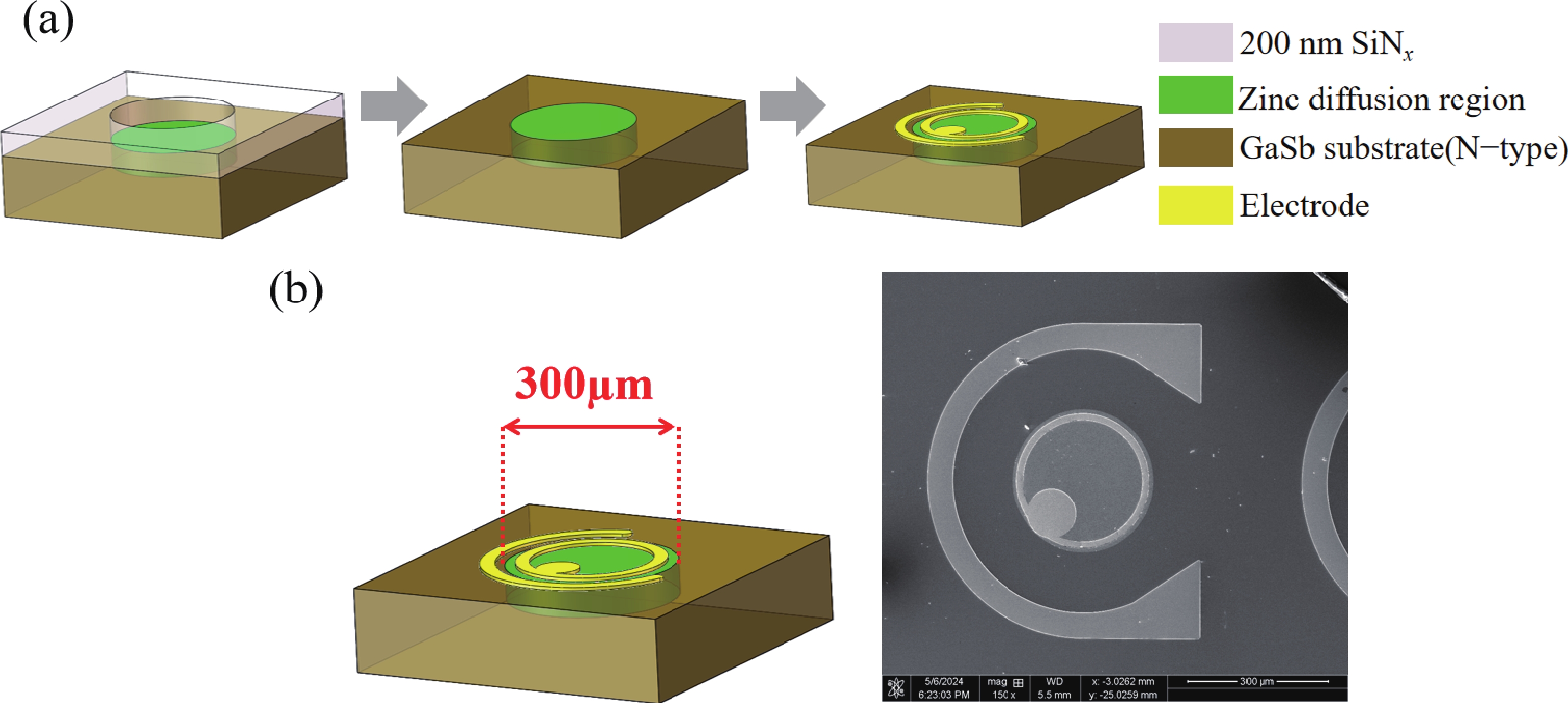
Fig. 1.
(Color online) (a) The process of planar structure photodiode fabrication through diffusion and the final device structure. (b) SEM diagram of the fabricated devices.
ARTICLES
Yuanzhi Cui1, 2, Hongyue Hao2, 3, , Shihao Zhang2, Shuo Wang2, Jing Zhang1, Yifan Shan2, 3, Ruoyu Xie2, 3, Xiaoyu Wang1, Chuang Wang1, Mengchen Liu1, Dongwei Jiang2, 3, Yingqiang Xu2, 3, Guowei Wang2, 3, Donghai Wu2, 3, Zhichuan Niu2, 3 and Derang Cao1
Corresponding author: Hongyue Hao, haohongyue@semi.ac.cn
Abstract: This paper examines GaSb short-wavelength infrared detectors employing planar PN junctions. The fabrication was based on the Zn diffusion process and the diffusion temperature was optimized. Characterization revealed a 50% cut-off wavelength of 1.73 μm, a maximum detectivity of 8.73 × 1010 cm·Hz1/2/W, and a minimum dark current density of 1.02 × 10⁻⁵ A/cm2. Additionally, a maximum quantum efficiency of 60.3% was achieved. Subsequent optimization of fabrication enabled the realization of a 320 × 256 focal plane array that exhibited satisfactory imaging results. Remarkably, the GaSb planar detectors demonstrated potential in low-cost short wavelength infrared imaging, without requiring material epitaxy or deposition.
Keywords: antimonide, short-wave infrared, planar junction, zinc diffusion
| [1] |
Zhang D, Lee D J, Desai A. Using short-wave infrared imaging for fruit quality evaluation. Intelligent Robots and Computer Vision XXXI: Algorithms and Techniques, 2014, 9025, 89 doi: 10.1117/12.2045406
|
| [2] |
Mo C, Kim G, Kim M S, et al. Discrimination methods for biological contaminants in fresh-cut lettuce based on VNIR and NIR hyperspectral imaging. Infrared Phys Technol, 2017, 85, 1 doi: 10.1016/j.infrared.2017.05.003
|
| [3] |
Jenal A, Bareth G, Bolten A, et al. Development of a VNIR/SWIR multispectral imaging system for vegetation monitoring with unmanned aerial vehicles. Sensors, 2019, 19, 5507 doi: 10.3390/s19245507
|
| [4] |
Hou F, Zhang Y, Zhou Y, et al. Review on infrared imaging technology. Sustainability, 2022, 14, 11161 doi: 10.3390/su141811161
|
| [5] |
Kütük M, Geneci İ, Özdemir O B, et al. Ground-based hyperspectral image surveillance system for explosive detection: methods, experiments, and comparisons. IEEE J Sel Top Appl Earth Obs Remote Sens, 2023, 16, 8747 doi: 10.1109/JSTARS.2023.3299730
|
| [6] |
Yang D, Lin J, Lin C, et al. Improved responsivity and detectivity of LPE HgCdTe short-wavelength infrared photodetector by tuning the composition gradient. Solid State Electron, 2023, 205, 108665 doi: 10.1016/j.sse.2023.108665
|
| [7] |
Dolas M H, Atesal O, Caliskan M D, et al. Low dark current diffusion limited planar type InGaAs photodetectors. Infrared Sensors, Devices, and Applications IX, 2019, 11129, 91 doi: 10.1117/12.2528666
|
| [8] |
Hoang A, Chen G, Haddadi A, et al. Demonstration of shortwavelength infrared photodiodes based on type-II InAs/GaSb/AlSb superlattices. Appl Phys Lett, 2012, 100, 211101 doi: 10.1063/1.4720094
|
| [9] |
Yan B, Liu W, Yu Z, et al. Temperature dynamic compensation vertical bridgman method growth of high-quality GaSb single crystals. J Cryst Growth, 2023, 602, 126988 doi: 10.1016/j.jcrysgro.2022.126988
|
| [10] |
Nunna K C, Tan S L, Reyner C J, et al. Short-wave infrared GaInAsSb photodiodes grown on GaAs substrate by interfacial misfit array technique. IEEE Photonics Technol Lett, 2011, 24, 218 doi: 10.1109/LPT.2011.2177253
|
| [11] |
Li J, Saroj R, Slivken S, et al. High performance planar antimony-based superlattice photodetectors using zinc diffusion grown by MBE. Photonics, 2022, 9, 664 doi: 10.3390/photonics9090664
|
| [12] |
Gray N W, Prax A, Johnson D, et al. Rapid development of high-volume manufacturing methods for epi-ready GaSb wafers up to 6” diameter for IR imaging applications. Infrared Technology and Applications XLII, 2016, 9819, 274 doi: 10.1117/12.2223998
|
| [13] |
Li Z H, Li H Y, Du H Y, et al. Study of InSb IRFPA with planar PN junctions. Laser Infrared, 2015, 45, 814 (in Chinese) doi: 10.3969/j.issn.1001-5078.2015.07.017
|
| [14] |
Lim K, Pham H, Yoon S, et al. InSb1-xNx/InSb/GaAs alloys by thermal annealing for midinfrared photodetection. Appl Phys Lett, 2010, 97, 221112 doi: 10.1063/1.3524228
|
| [15] |
Kang Z, Qiu G C. InSb IRFPA detector chip with planar PN junction based on thermal diffusion method. Laser Infrared, 2014, 44, 757 (in Chinese) doi: 10.3969/j.issn.1001-5078.2014.06.011
|
| [16] |
Simcock M N, Santailler J L, Dusserre P, et al. Zinc diffusion in GaSb for thermophotovoltaic cell applications. AIP Conf Proc, 2004, 738, 303 doi: 10.1063/1.1841907
|
| [17] |
Newell A, Logan J, Carrasco R, et al. Effects of doping and minority carrier lifetime on mid-wave infrared InGaAs/InAsSb superlattice nBn detector performance. Appl Phys Lett, 2023, 122, 171102 doi: 10.1063/5.0136409
|
| [18] |
Hao H, Wang G, Xiang W, et al. Fabrication of type-II InAs/GaSb superlattice long-wavelength infrared focal plane arrays. Infrared Phys Technol, 2015, 72, 276 doi: 10.1016/j.infrared.2015.07.025
|
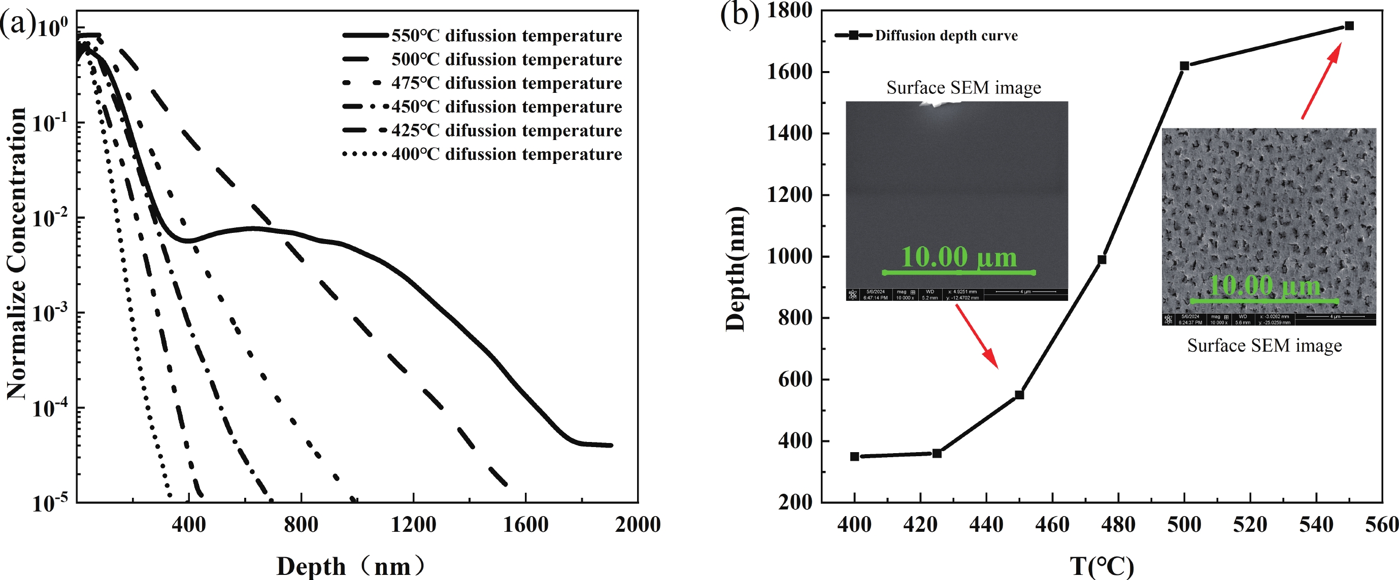
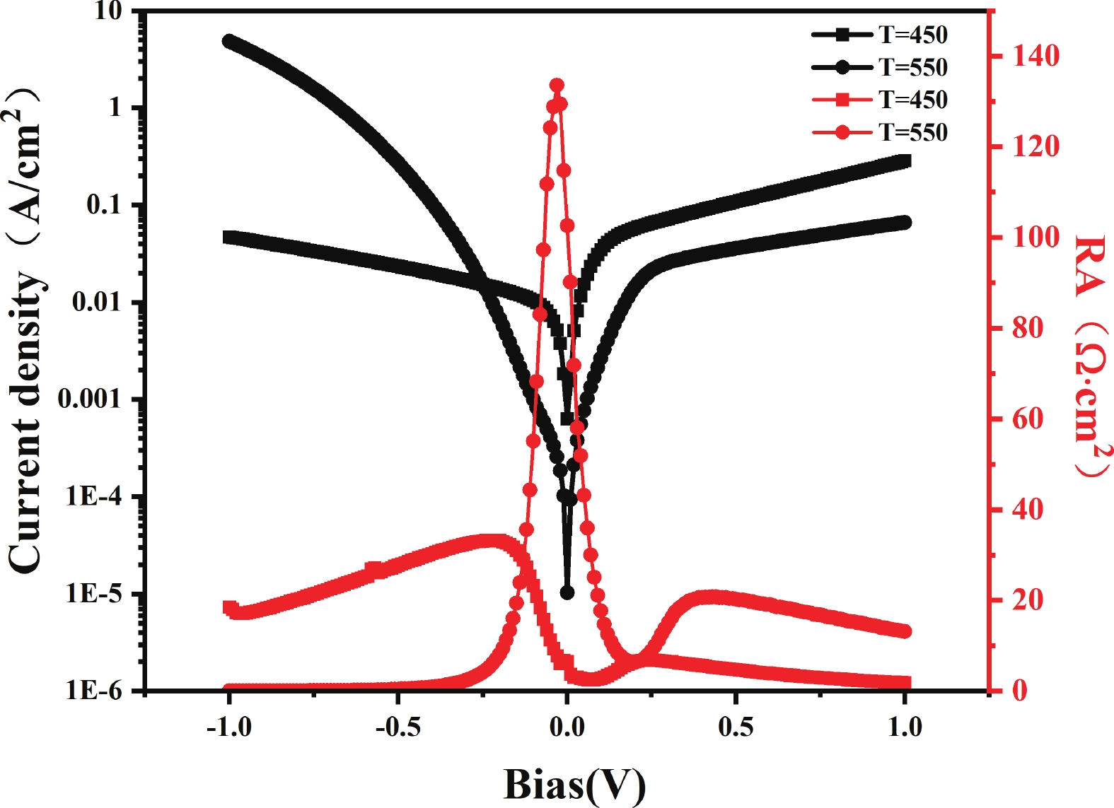
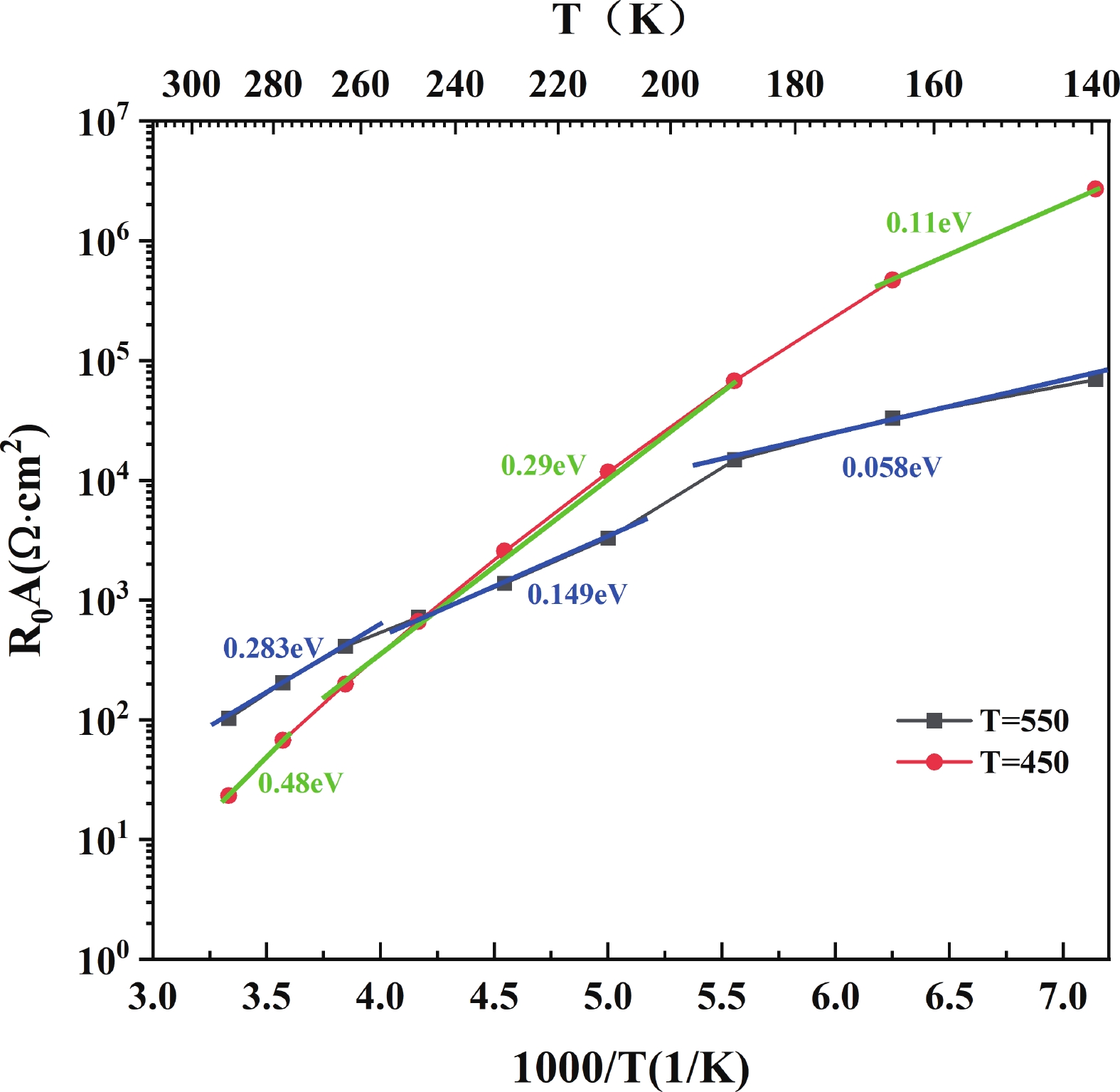
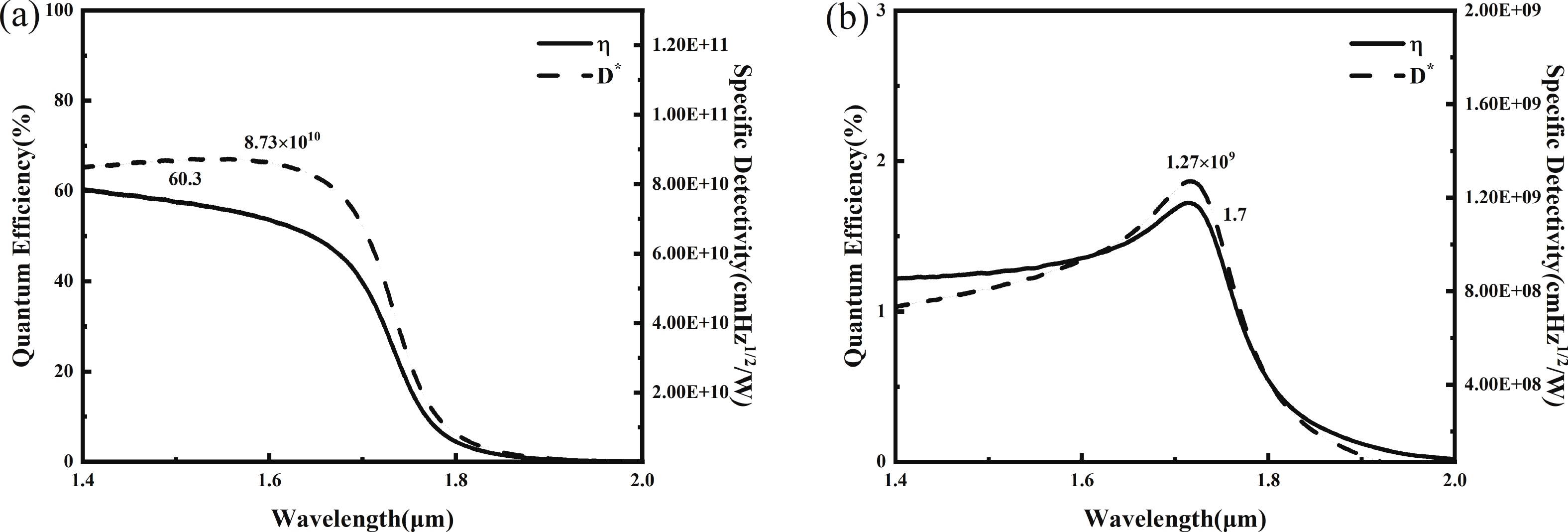
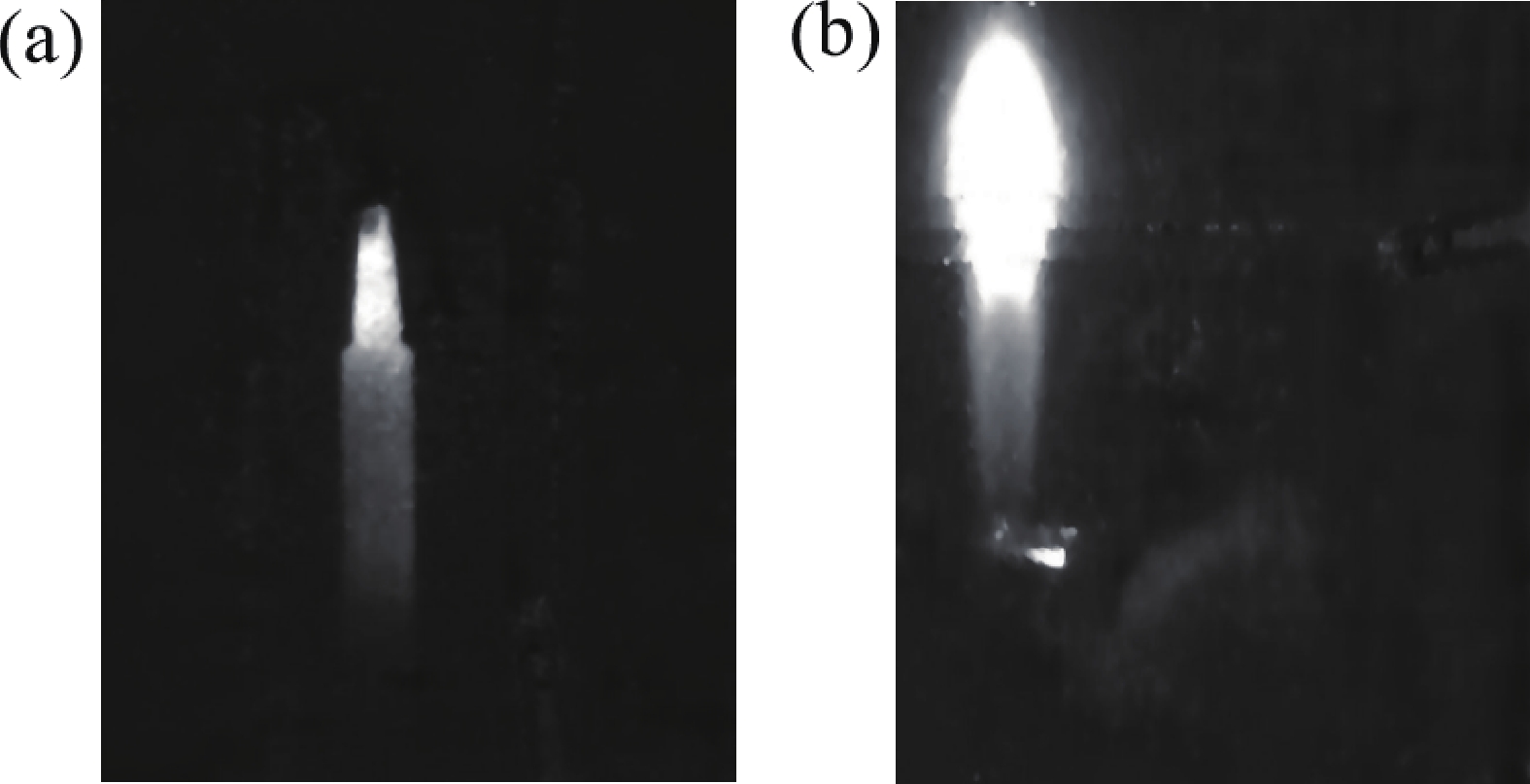
Table 1. Performance comparison of planar junction detectors at different diffusion temperatures.
| Diffusion temperature (°C) | Test temperature (K) | R0A (Ω·cm2) | η (%) | D* (cm·Hz1/2/W) |
| 450 | 300 | 30.3 | 1.7 | 1.27 × 10⁹ |
| 550 | 300 | 133.5 | 60.3 | 8.73 × 10¹⁰ |
 DownLoad: CSV
| [1] |
Zhang D, Lee D J, Desai A. Using short-wave infrared imaging for fruit quality evaluation. Intelligent Robots and Computer Vision XXXI: Algorithms and Techniques, 2014, 9025, 89 doi: 10.1117/12.2045406
|
| [2] |
Mo C, Kim G, Kim M S, et al. Discrimination methods for biological contaminants in fresh-cut lettuce based on VNIR and NIR hyperspectral imaging. Infrared Phys Technol, 2017, 85, 1 doi: 10.1016/j.infrared.2017.05.003
|
| [3] |
Jenal A, Bareth G, Bolten A, et al. Development of a VNIR/SWIR multispectral imaging system for vegetation monitoring with unmanned aerial vehicles. Sensors, 2019, 19, 5507 doi: 10.3390/s19245507
|
| [4] |
Hou F, Zhang Y, Zhou Y, et al. Review on infrared imaging technology. Sustainability, 2022, 14, 11161 doi: 10.3390/su141811161
|
| [5] |
Kütük M, Geneci İ, Özdemir O B, et al. Ground-based hyperspectral image surveillance system for explosive detection: methods, experiments, and comparisons. IEEE J Sel Top Appl Earth Obs Remote Sens, 2023, 16, 8747 doi: 10.1109/JSTARS.2023.3299730
|
| [6] |
Yang D, Lin J, Lin C, et al. Improved responsivity and detectivity of LPE HgCdTe short-wavelength infrared photodetector by tuning the composition gradient. Solid State Electron, 2023, 205, 108665 doi: 10.1016/j.sse.2023.108665
|
| [7] |
Dolas M H, Atesal O, Caliskan M D, et al. Low dark current diffusion limited planar type InGaAs photodetectors. Infrared Sensors, Devices, and Applications IX, 2019, 11129, 91 doi: 10.1117/12.2528666
|
| [8] |
Hoang A, Chen G, Haddadi A, et al. Demonstration of shortwavelength infrared photodiodes based on type-II InAs/GaSb/AlSb superlattices. Appl Phys Lett, 2012, 100, 211101 doi: 10.1063/1.4720094
|
| [9] |
Yan B, Liu W, Yu Z, et al. Temperature dynamic compensation vertical bridgman method growth of high-quality GaSb single crystals. J Cryst Growth, 2023, 602, 126988 doi: 10.1016/j.jcrysgro.2022.126988
|
| [10] |
Nunna K C, Tan S L, Reyner C J, et al. Short-wave infrared GaInAsSb photodiodes grown on GaAs substrate by interfacial misfit array technique. IEEE Photonics Technol Lett, 2011, 24, 218 doi: 10.1109/LPT.2011.2177253
|
| [11] |
Li J, Saroj R, Slivken S, et al. High performance planar antimony-based superlattice photodetectors using zinc diffusion grown by MBE. Photonics, 2022, 9, 664 doi: 10.3390/photonics9090664
|
| [12] |
Gray N W, Prax A, Johnson D, et al. Rapid development of high-volume manufacturing methods for epi-ready GaSb wafers up to 6” diameter for IR imaging applications. Infrared Technology and Applications XLII, 2016, 9819, 274 doi: 10.1117/12.2223998
|
| [13] |
Li Z H, Li H Y, Du H Y, et al. Study of InSb IRFPA with planar PN junctions. Laser Infrared, 2015, 45, 814 (in Chinese) doi: 10.3969/j.issn.1001-5078.2015.07.017
|
| [14] |
Lim K, Pham H, Yoon S, et al. InSb1-xNx/InSb/GaAs alloys by thermal annealing for midinfrared photodetection. Appl Phys Lett, 2010, 97, 221112 doi: 10.1063/1.3524228
|
| [15] |
Kang Z, Qiu G C. InSb IRFPA detector chip with planar PN junction based on thermal diffusion method. Laser Infrared, 2014, 44, 757 (in Chinese) doi: 10.3969/j.issn.1001-5078.2014.06.011
|
| [16] |
Simcock M N, Santailler J L, Dusserre P, et al. Zinc diffusion in GaSb for thermophotovoltaic cell applications. AIP Conf Proc, 2004, 738, 303 doi: 10.1063/1.1841907
|
| [17] |
Newell A, Logan J, Carrasco R, et al. Effects of doping and minority carrier lifetime on mid-wave infrared InGaAs/InAsSb superlattice nBn detector performance. Appl Phys Lett, 2023, 122, 171102 doi: 10.1063/5.0136409
|
| [18] |
Hao H, Wang G, Xiang W, et al. Fabrication of type-II InAs/GaSb superlattice long-wavelength infrared focal plane arrays. Infrared Phys Technol, 2015, 72, 276 doi: 10.1016/j.infrared.2015.07.025
|


Article views: 1636 Times PDF downloads: 112 Times Cited by: 0 Times
Received: 16 April 2024 Revised: 21 May 2024 Online: Accepted Manuscript: 11 June 2024Uncorrected proof: 11 June 2024Published: 15 September 2024
| Citation: |
Yuanzhi Cui, Hongyue Hao, Shihao Zhang, Shuo Wang, Jing Zhang, Yifan Shan, Ruoyu Xie, Xiaoyu Wang, Chuang Wang, Mengchen Liu, Dongwei Jiang, Yingqiang Xu, Guowei Wang, Donghai Wu, Zhichuan Niu, Derang Cao. High-performance GaSb planar PN junction detector[J]. Journal of Semiconductors, 2024, 45(9): 092403. doi: 10.1088/1674-4926/24040024
****
Y Z Cui, H Y Hao, S H Zhang, S Wang, J Zhang, Y F Shan, R Y Xie, X Y Wang, C Wang, M C Liu, D W Jiang, Y Q Xu, G W Wang, D H Wu, Z C Niu, and D R Cao, High-performance GaSb planar PN junction detector[J]. J. Semicond., 2024, 45(9), 092403 doi: 10.1088/1674-4926/24040024

|
 Yuanzhi Cui received a bachelor’s degree from North China University of Technology, Beijing, China, in 2021. He is currently pursuing a master’s degree with the Qingdao University, Qingdao, China. His present research interests include short−wave infrared detector of antimonide
 Hongyue Hao received her doctoral degree from the Institute of Semiconductors, Chinese Academy of Sciences in 2018. Following her PhD, she worked as a postdoctoral researcher in the Juelich Research Center in Germany. She is currently a Youth Researcher at the Institute of Semiconductors, Chinese Academy of Sciences. Her research focused on the Sb-based infrared detectors, especially including the broadband and multi-band detectors with meta-surface, low-cost, low noise and high sensitivity detectors
| [1] |
Zhang D, Lee D J, Desai A. Using short-wave infrared imaging for fruit quality evaluation. Intelligent Robots and Computer Vision XXXI: Algorithms and Techniques, 2014, 9025, 89 doi: 10.1117/12.2045406
|
| [2] |
Mo C, Kim G, Kim M S, et al. Discrimination methods for biological contaminants in fresh-cut lettuce based on VNIR and NIR hyperspectral imaging. Infrared Phys Technol, 2017, 85, 1 doi: 10.1016/j.infrared.2017.05.003
|
| [3] |
Jenal A, Bareth G, Bolten A, et al. Development of a VNIR/SWIR multispectral imaging system for vegetation monitoring with unmanned aerial vehicles. Sensors, 2019, 19, 5507 doi: 10.3390/s19245507
|
| [4] |
Hou F, Zhang Y, Zhou Y, et al. Review on infrared imaging technology. Sustainability, 2022, 14, 11161 doi: 10.3390/su141811161
|
| [5] |
Kütük M, Geneci İ, Özdemir O B, et al. Ground-based hyperspectral image surveillance system for explosive detection: methods, experiments, and comparisons. IEEE J Sel Top Appl Earth Obs Remote Sens, 2023, 16, 8747 doi: 10.1109/JSTARS.2023.3299730
|
| [6] |
Yang D, Lin J, Lin C, et al. Improved responsivity and detectivity of LPE HgCdTe short-wavelength infrared photodetector by tuning the composition gradient. Solid State Electron, 2023, 205, 108665 doi: 10.1016/j.sse.2023.108665
|
| [7] |
Dolas M H, Atesal O, Caliskan M D, et al. Low dark current diffusion limited planar type InGaAs photodetectors. Infrared Sensors, Devices, and Applications IX, 2019, 11129, 91 doi: 10.1117/12.2528666
|
| [8] |
Hoang A, Chen G, Haddadi A, et al. Demonstration of shortwavelength infrared photodiodes based on type-II InAs/GaSb/AlSb superlattices. Appl Phys Lett, 2012, 100, 211101 doi: 10.1063/1.4720094
|
| [9] |
Yan B, Liu W, Yu Z, et al. Temperature dynamic compensation vertical bridgman method growth of high-quality GaSb single crystals. J Cryst Growth, 2023, 602, 126988 doi: 10.1016/j.jcrysgro.2022.126988
|
| [10] |
Nunna K C, Tan S L, Reyner C J, et al. Short-wave infrared GaInAsSb photodiodes grown on GaAs substrate by interfacial misfit array technique. IEEE Photonics Technol Lett, 2011, 24, 218 doi: 10.1109/LPT.2011.2177253
|
| [11] |
Li J, Saroj R, Slivken S, et al. High performance planar antimony-based superlattice photodetectors using zinc diffusion grown by MBE. Photonics, 2022, 9, 664 doi: 10.3390/photonics9090664
|
| [12] |
Gray N W, Prax A, Johnson D, et al. Rapid development of high-volume manufacturing methods for epi-ready GaSb wafers up to 6” diameter for IR imaging applications. Infrared Technology and Applications XLII, 2016, 9819, 274 doi: 10.1117/12.2223998
|
| [13] |
Li Z H, Li H Y, Du H Y, et al. Study of InSb IRFPA with planar PN junctions. Laser Infrared, 2015, 45, 814 (in Chinese) doi: 10.3969/j.issn.1001-5078.2015.07.017
|
| [14] |
Lim K, Pham H, Yoon S, et al. InSb1-xNx/InSb/GaAs alloys by thermal annealing for midinfrared photodetection. Appl Phys Lett, 2010, 97, 221112 doi: 10.1063/1.3524228
|
| [15] |
Kang Z, Qiu G C. InSb IRFPA detector chip with planar PN junction based on thermal diffusion method. Laser Infrared, 2014, 44, 757 (in Chinese) doi: 10.3969/j.issn.1001-5078.2014.06.011
|
| [16] |
Simcock M N, Santailler J L, Dusserre P, et al. Zinc diffusion in GaSb for thermophotovoltaic cell applications. AIP Conf Proc, 2004, 738, 303 doi: 10.1063/1.1841907
|
| [17] |
Newell A, Logan J, Carrasco R, et al. Effects of doping and minority carrier lifetime on mid-wave infrared InGaAs/InAsSb superlattice nBn detector performance. Appl Phys Lett, 2023, 122, 171102 doi: 10.1063/5.0136409
|
| [18] |
Hao H, Wang G, Xiang W, et al. Fabrication of type-II InAs/GaSb superlattice long-wavelength infrared focal plane arrays. Infrared Phys Technol, 2015, 72, 276 doi: 10.1016/j.infrared.2015.07.025
|

 WeChat ID
Journal of Semiconductors © 2017 All Rights Reserved 京ICP备05085259号-2


