


Fig. 1.
(Color online) (a) Schematic illustration of the device structure and fabrication process flow. (b) Schematic diagram of the synaptic information transmission in neurons. (c) The X-ray photoelectron spectroscopy (XPS).
ARTICLES
Jieru Song1, Jialin Meng1, , Tianyu Wang2, 3, Changjin Wan4, Hao Zhu1, Qingqing Sun1, David Wei Zhang1 and Lin Chen1, 3, 5,
Corresponding author: Jialin Meng, jlmeng@fudan.edu.cn; Lin Chen, linchen@fudan.edu.cn
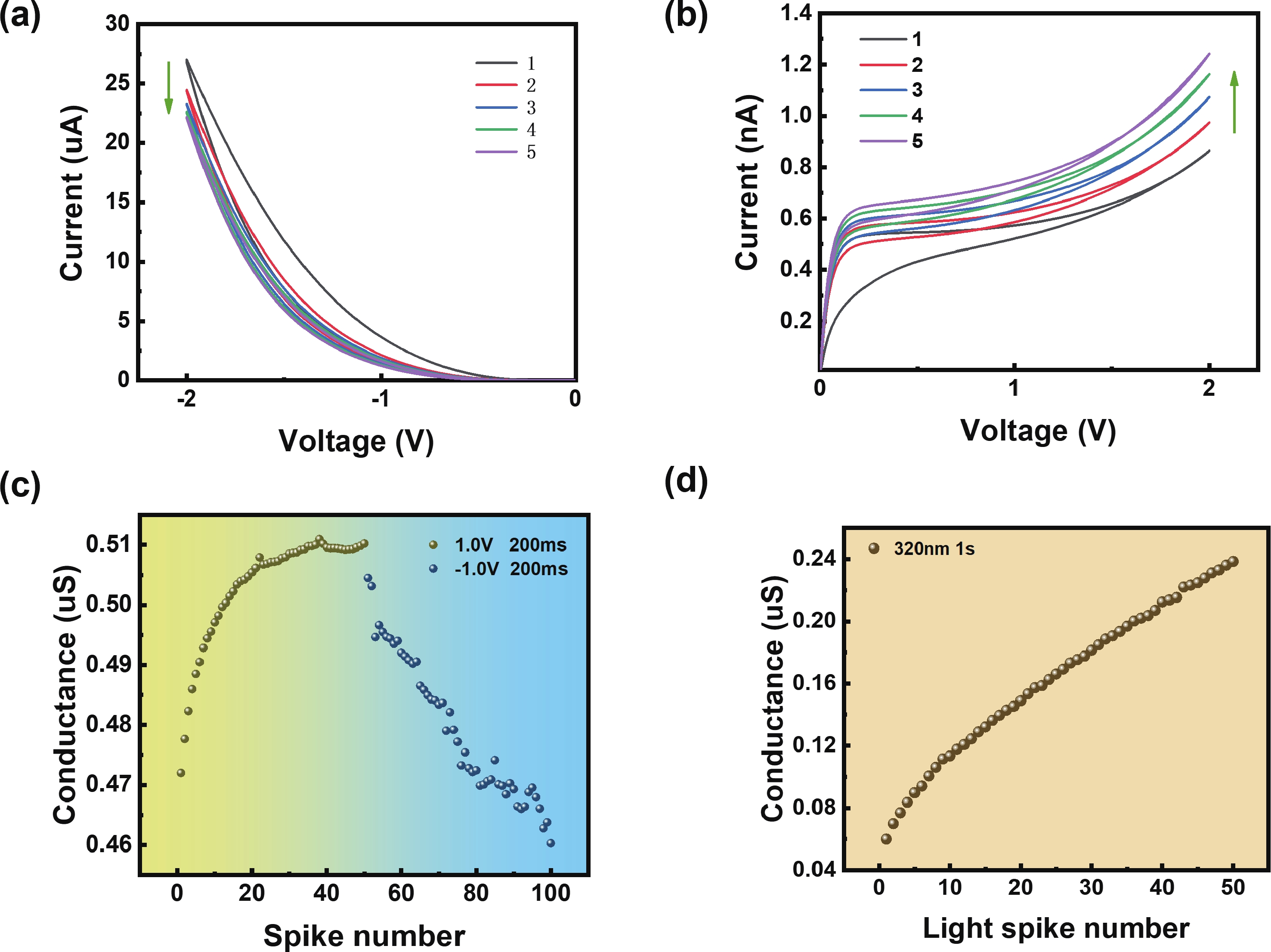
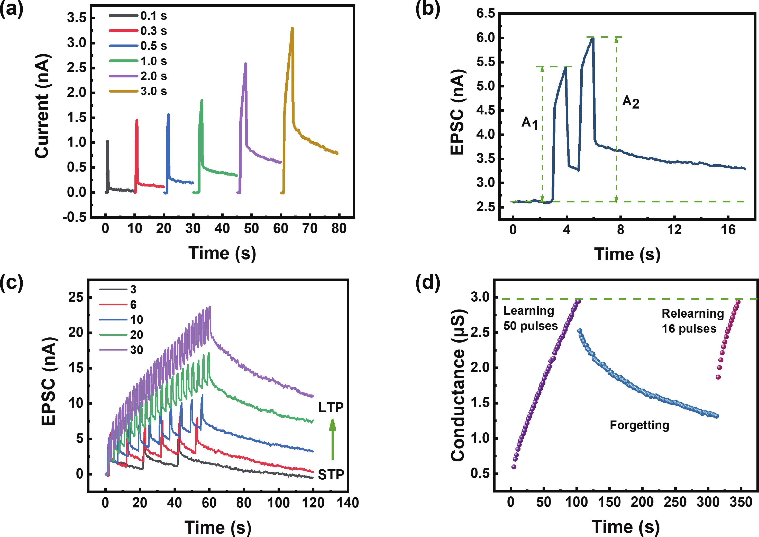
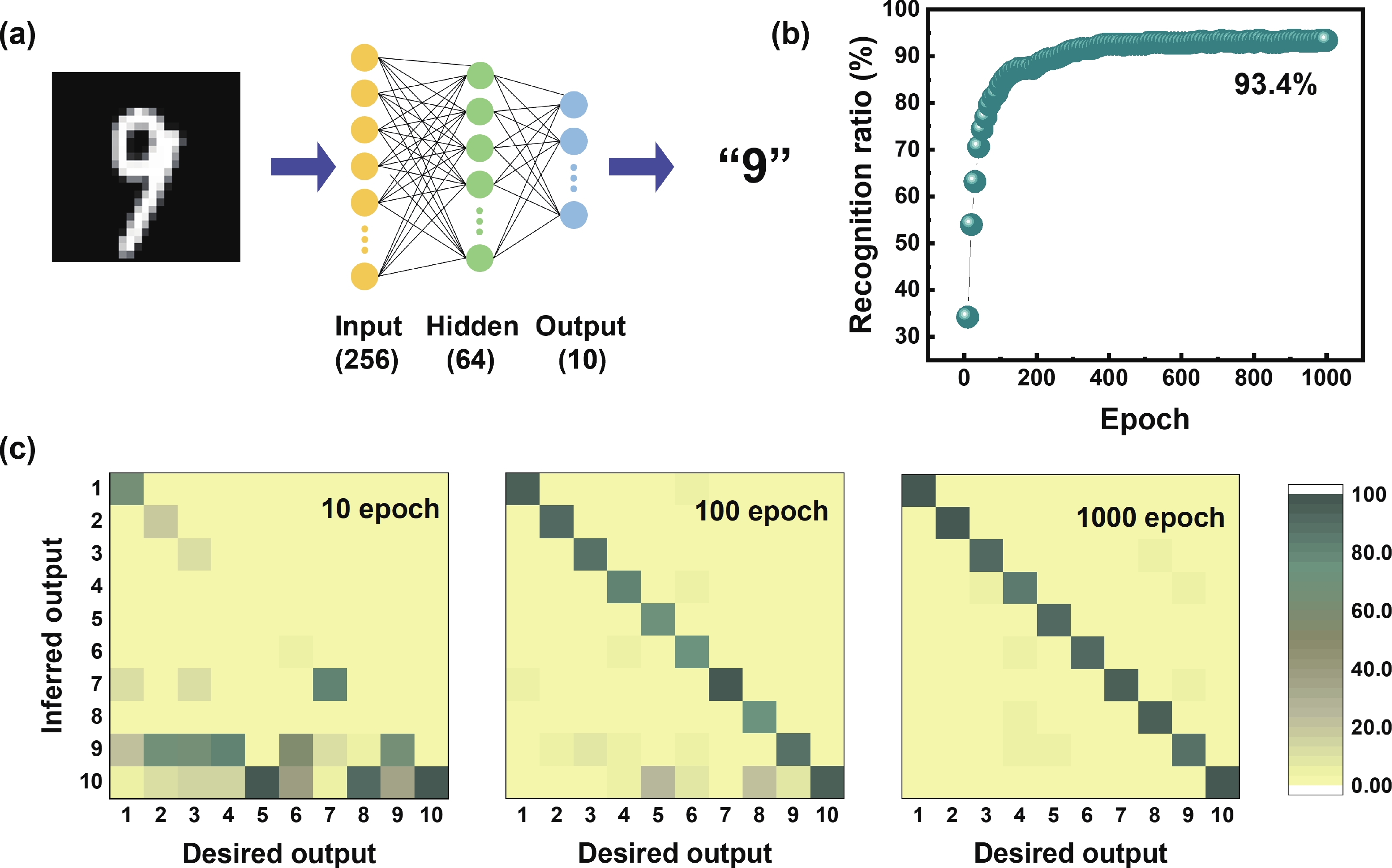
Abstract: Photoelectric synaptic devices could emulate synaptic behaviors utilizing photoelectric effects and offer promising prospects with their high-speed operation and low crosstalk. In this study, we introduced a novel InGaZnO-based photoelectric memristor. Under both electrical and optical stimulation, the device successfully emulated synaptic characteristics including excitatory postsynaptic current (EPSC), paired-pulse facilitation (PPF), long-term potentiation (LTP), and long-term depression (LTD). Furthermore, we demonstrated the practical application of our synaptic devices through the recognition of handwritten digits. The devices have successfully shown their ability to modulate synaptic weights effectively through light pulse stimulation, resulting in a recognition accuracy of up to 93.4%. The results illustrated the potential of IGZO-based memristors in neuromorphic computing, particularly their ability to simulate synaptic functionalities and contribute to image recognition tasks.
Keywords: InGaZnO, artificial synapse, neuromorphic computing, photoelectric memristor
| [1] |
Shastri B J, Tait A N, Ferreira de Lima T, et al. Photonics for artificial intelligence and neuromorphic computing. Nat Photonics, 2021, 15, 102 doi: 10.1038/s41566-020-00754-y
|
| [2] |
Tian B B, Xie Z Z, Chen L Q, et al. Ultralow-power in-memory computing based on ferroelectric memcapacitor network. Exploration, 2023, 3, 20220126 doi: 10.1002/EXP.20220126
|
| [3] |
Schuman C D, Kulkarni S R, Parsa M, et al. Opportunities for neuromorphic computing algorithms and applications. Nat Comput Sci, 2022, 2, 10 doi: 10.1038/s43588-021-00184-y
|
| [4] |
Furber S B, Lester D R, Plana L A, et al. Overview of the SpiNNaker system architecture. IEEE Trans Comput, 2013, 62, 2454 doi: 10.1109/TC.2012.142
|
| [5] |
Meng J L, Wang T Y, Zhu H, et al. Integrated In-sensor computing optoelectronic device for environment-adaptable artificial retina perception application. Nano Lett, 2022, 22, 81 doi: 10.1021/acs.nanolett.1c03240
|
| [6] |
Wang T Y, Meng J L, Zhou X F, et al. Reconfigurable neuromorphic memristor network for ultralow-power smart textile electronics. Nat Commun, 2022, 13, 7432 doi: 10.1038/s41467-022-35160-1
|
| [7] |
Zhang J Y, Dai S L, Zhao Y W, et al. Recent progress in photonic synapses for neuromorphic systems. Adv Intell Syst, 2020, 2, 1900136 doi: 10.1002/aisy.201900136
|
| [8] |
Ma F M, Zhu Y B, Xu Z W, et al. Optoelectronic perovskite synapses for neuromorphic computing. Adv Funct Materials, 2020, 30, 1908901 doi: 10.1002/adfm.201908901
|
| [9] |
Meng J L, Wang T Y, Chen L, et al. Energy-efficient flexible photoelectric device with 2D/0D hybrid structure for bio-inspired artificial heterosynapse application. Nano Energy, 2021, 83, 105815 doi: 10.1016/j.nanoen.2021.105815
|
| [10] |
Liu Y, Wang T, Xu K, et al. Low-power and high-speed HfLaO-based FE-TFTs for artificial synapse and reconfigurable logic applications. Mater Horiz, 2024, 11, 490 doi: 10.1039/D3MH01461D
|
| [11] |
Kwon J Y, Kim J E, Kim J S, et al. Artificial sensory system based on memristive devices. Exploration, 2024, 4, 20220162 doi: 10.1002/EXP.20220162
|
| [12] |
Fang Y Q, Meng J L, Li Q X, et al. Two-terminal photoelectric dual modulation synaptic devices for face recognition. IEEE Electron Device Lett, 2023, 44, 241 doi: 10.1109/LED.2022.3228944
|
| [13] |
Cheng Y C, Li H, Liu B, et al. Vertical 0D-perovskite/2D-MoS2 van der waals heterojunction phototransistor for emulating photoelectric-synergistically classical Pavlovian conditioning and neural coding dynamics. Small, 2020, 16, 2005217 doi: 10.1002/smll.202005217
|
| [14] |
Wang T Y, Meng J L, He Z Y, et al. Ultralow power wearable heterosynapse with photoelectric synergistic modulation. Adv Sci, 2020, 7, 1903480 doi: 10.1002/advs.201903480
|
| [15] |
Jeon J H, Gong T K, Kong Y M, et al. Effect of post-deposition annealing on the structural, optical and electrical properties of IGZO films. Electron Mater Lett, 2015, 11, 481 doi: 10.1007/s13391-014-4410-1
|
| [16] |
Kumar N, Patel M, Nguyen T T, et al. All-oxide-based and metallic electrode-free artificial synapses for transparent neuromorphic computing. Materials Today Chemistry, 2022, 23, 100681 doi: 10.1016/j.mtchem.2021.100681
|
| [17] |
Wang J Y, Leng Y M, Zhao T C, et al. SnO2-based optoelectronic synapses for artificial visual applications. J Phys: Conf Ser, 2023, 2524, 012011 doi: 10.1088/1742-6596/2524/1/012011
|
| [18] |
Wang T Y, Meng J L, He Z Y, et al. Fully transparent, flexible and waterproof synapses with pattern recognition in organic environments. Nanoscale Horizons, 2019, 4, 1293 doi: 10.1039/C9NH00341J
|
| [19] |
Wang T Y, He Z Y, Chen L, et al. An organic flexible artificial bio-synapses with long-term plasticity for neuromorphic computing. Micromachines, 2018, 9, 239 doi: 10.3390/mi9050239
|
| [20] |
Cheng Z G, Ríos C, Pernice W H P, et al. On-chip photonic synapse. Sci Adv, 2017, 3, e1700160 doi: 10.1126/sciadv.1700160
|
| [21] |
Li G, Xie D G, Zhong H, et al. Photo-induced non-volatile VO2 phase transition for neuromorphic ultraviolet sensors. Nat Commun, 2022, 13, 1729 doi: 10.1038/s41467-022-29456-5
|
| [22] |
Pérez-Tomás A. Functional oxides for photoneuromorphic engineering: Toward a solar brain. Adv Materials Inter, 2019, 6, 1900471 doi: 10.1002/admi.201900471
|
| [23] |
Wang Y, Yin L, Huang W, et al. Optoelectronic synaptic devices for neuromorphic computing. Adv Intell Syst, 2021, 3, 2000099 doi: 10.1002/aisy.202000099
|
| [24] |
Hara Y, Kikuchi T, Kitagawa H, et al. IGZO-TFT technology for large-screen 8K display. J Soc Info Display, 2018, 26, 169 doi: 10.1002/jsid.648
|
| [25] |
Kamiya T, Hosono H. Material characteristics and applications of transparent amorphous oxide semiconductors. NPG Asia Mater, 2010, 2, 15 doi: 10.1038/asiamat.2010.5
|
| [26] |
Hsieh H H, Lu H H, Ting H C, et al. Development of IGZO TFTs and their applications to next-generation flat-panel displays. J Inf Disp, 2010, 11, 160 doi: 10.1080/15980316.2010.9665845
|
| [27] |
Zhu Y X, Peng B C, Zhu L, et al. IGZO nanofiber photoelectric neuromorphic transistors with indium ratio tuned synaptic plasticity. Appl Phys Lett, 2022, 121, 133502 doi: 10.1063/5.0109772
|
| [28] |
Ke S, He Y L, Zhu L Q, et al. Indium-gallium-zinc-oxide based photoelectric neuromorphic transistors for modulable photoexcited corneal nociceptor emulation. Adv Electron Mater, 2021, 7, 2100487 doi: 10.1002/aelm.202100487
|
| [29] |
Tran M D, Kim H, Kim J S, et al. Two-terminal multibit optical memory via van der waals heterostructure. Adv Mater, 2019, 31, 1807075 doi: 10.1002/adma.201807075
|
| [30] |
Tuchman Y, Mangoma T N, Gkoupidenis P, et al. Organic neuromorphic devices: Past, present, and future challenges. MRS Bull, 2020, 45, 619 doi: 10.1557/mrs.2020.196
|
| [31] |
LeCun Y, Bottou L, Bengio Y, et al. Gradient-based learning applied to document recognition. Proc IEEE, 1998, 86, 2278 doi: 10.1109/5.726791
|


Article views: 2566 Times PDF downloads: 163 Times Cited by: 0 Times
Received: 26 April 2024 Revised: 10 May 2024 Online: Accepted Manuscript: 04 June 2024Uncorrected proof: 05 June 2024Published: 15 September 2024
| Citation: |
Jieru Song, Jialin Meng, Tianyu Wang, Changjin Wan, Hao Zhu, Qingqing Sun, David Wei Zhang, Lin Chen. InGaZnO-based photoelectric synaptic devices for neuromorphic computing[J]. Journal of Semiconductors, 2024, 45(9): 092402. doi: 10.1088/1674-4926/24040038
****
J R Song, J L Meng, T Y Wang, C J Wan, H Zhu, Q Q Sun, D W Zhang, and L Chen, InGaZnO-based photoelectric synaptic devices for neuromorphic computing[J]. J. Semicond., 2024, 45(9), 092402 doi: 10.1088/1674-4926/24040038

|
 Jieru Song is currently a master's student at the School of Microelectronics, Fudan University, under the supervision of Prof. Lin Chen. She received her bachelor's degree in 2022 from the School of Electronic Science and Engineering, Nanjing University. Her research focuses on photoelectric memristors and neuromorphic computing
 Jialin Meng received her Ph.D degree in microelectronics and solid-state electronics from Fudan University, Shanghai, China in 2022. She is currently a Postdoctor in the School of Microelectronics, Fudan University. Her research focuses on the optoelectronic neuromorphic devices, in-sensor computing, and flexible electronics
 Lin Chen (February 1986) received the Ph.D degree in microelectronics and solid-state electronics from Fudan University, Shanghai, China in 2012. He is currently a Professor in the School of Microelectronics, Fudan University. His research interests include semiconductor devices, as well as advanced CMOS process and 3D IC technology. He has (co) authored over 150 articles in international refereed journals
| [1] |
Shastri B J, Tait A N, Ferreira de Lima T, et al. Photonics for artificial intelligence and neuromorphic computing. Nat Photonics, 2021, 15, 102 doi: 10.1038/s41566-020-00754-y
|
| [2] |
Tian B B, Xie Z Z, Chen L Q, et al. Ultralow-power in-memory computing based on ferroelectric memcapacitor network. Exploration, 2023, 3, 20220126 doi: 10.1002/EXP.20220126
|
| [3] |
Schuman C D, Kulkarni S R, Parsa M, et al. Opportunities for neuromorphic computing algorithms and applications. Nat Comput Sci, 2022, 2, 10 doi: 10.1038/s43588-021-00184-y
|
| [4] |
Furber S B, Lester D R, Plana L A, et al. Overview of the SpiNNaker system architecture. IEEE Trans Comput, 2013, 62, 2454 doi: 10.1109/TC.2012.142
|
| [5] |
Meng J L, Wang T Y, Zhu H, et al. Integrated In-sensor computing optoelectronic device for environment-adaptable artificial retina perception application. Nano Lett, 2022, 22, 81 doi: 10.1021/acs.nanolett.1c03240
|
| [6] |
Wang T Y, Meng J L, Zhou X F, et al. Reconfigurable neuromorphic memristor network for ultralow-power smart textile electronics. Nat Commun, 2022, 13, 7432 doi: 10.1038/s41467-022-35160-1
|
| [7] |
Zhang J Y, Dai S L, Zhao Y W, et al. Recent progress in photonic synapses for neuromorphic systems. Adv Intell Syst, 2020, 2, 1900136 doi: 10.1002/aisy.201900136
|
| [8] |
Ma F M, Zhu Y B, Xu Z W, et al. Optoelectronic perovskite synapses for neuromorphic computing. Adv Funct Materials, 2020, 30, 1908901 doi: 10.1002/adfm.201908901
|
| [9] |
Meng J L, Wang T Y, Chen L, et al. Energy-efficient flexible photoelectric device with 2D/0D hybrid structure for bio-inspired artificial heterosynapse application. Nano Energy, 2021, 83, 105815 doi: 10.1016/j.nanoen.2021.105815
|
| [10] |
Liu Y, Wang T, Xu K, et al. Low-power and high-speed HfLaO-based FE-TFTs for artificial synapse and reconfigurable logic applications. Mater Horiz, 2024, 11, 490 doi: 10.1039/D3MH01461D
|
| [11] |
Kwon J Y, Kim J E, Kim J S, et al. Artificial sensory system based on memristive devices. Exploration, 2024, 4, 20220162 doi: 10.1002/EXP.20220162
|
| [12] |
Fang Y Q, Meng J L, Li Q X, et al. Two-terminal photoelectric dual modulation synaptic devices for face recognition. IEEE Electron Device Lett, 2023, 44, 241 doi: 10.1109/LED.2022.3228944
|
| [13] |
Cheng Y C, Li H, Liu B, et al. Vertical 0D-perovskite/2D-MoS2 van der waals heterojunction phototransistor for emulating photoelectric-synergistically classical Pavlovian conditioning and neural coding dynamics. Small, 2020, 16, 2005217 doi: 10.1002/smll.202005217
|
| [14] |
Wang T Y, Meng J L, He Z Y, et al. Ultralow power wearable heterosynapse with photoelectric synergistic modulation. Adv Sci, 2020, 7, 1903480 doi: 10.1002/advs.201903480
|
| [15] |
Jeon J H, Gong T K, Kong Y M, et al. Effect of post-deposition annealing on the structural, optical and electrical properties of IGZO films. Electron Mater Lett, 2015, 11, 481 doi: 10.1007/s13391-014-4410-1
|
| [16] |
Kumar N, Patel M, Nguyen T T, et al. All-oxide-based and metallic electrode-free artificial synapses for transparent neuromorphic computing. Materials Today Chemistry, 2022, 23, 100681 doi: 10.1016/j.mtchem.2021.100681
|
| [17] |
Wang J Y, Leng Y M, Zhao T C, et al. SnO2-based optoelectronic synapses for artificial visual applications. J Phys: Conf Ser, 2023, 2524, 012011 doi: 10.1088/1742-6596/2524/1/012011
|
| [18] |
Wang T Y, Meng J L, He Z Y, et al. Fully transparent, flexible and waterproof synapses with pattern recognition in organic environments. Nanoscale Horizons, 2019, 4, 1293 doi: 10.1039/C9NH00341J
|
| [19] |
Wang T Y, He Z Y, Chen L, et al. An organic flexible artificial bio-synapses with long-term plasticity for neuromorphic computing. Micromachines, 2018, 9, 239 doi: 10.3390/mi9050239
|
| [20] |
Cheng Z G, Ríos C, Pernice W H P, et al. On-chip photonic synapse. Sci Adv, 2017, 3, e1700160 doi: 10.1126/sciadv.1700160
|
| [21] |
Li G, Xie D G, Zhong H, et al. Photo-induced non-volatile VO2 phase transition for neuromorphic ultraviolet sensors. Nat Commun, 2022, 13, 1729 doi: 10.1038/s41467-022-29456-5
|
| [22] |
Pérez-Tomás A. Functional oxides for photoneuromorphic engineering: Toward a solar brain. Adv Materials Inter, 2019, 6, 1900471 doi: 10.1002/admi.201900471
|
| [23] |
Wang Y, Yin L, Huang W, et al. Optoelectronic synaptic devices for neuromorphic computing. Adv Intell Syst, 2021, 3, 2000099 doi: 10.1002/aisy.202000099
|
| [24] |
Hara Y, Kikuchi T, Kitagawa H, et al. IGZO-TFT technology for large-screen 8K display. J Soc Info Display, 2018, 26, 169 doi: 10.1002/jsid.648
|
| [25] |
Kamiya T, Hosono H. Material characteristics and applications of transparent amorphous oxide semiconductors. NPG Asia Mater, 2010, 2, 15 doi: 10.1038/asiamat.2010.5
|
| [26] |
Hsieh H H, Lu H H, Ting H C, et al. Development of IGZO TFTs and their applications to next-generation flat-panel displays. J Inf Disp, 2010, 11, 160 doi: 10.1080/15980316.2010.9665845
|
| [27] |
Zhu Y X, Peng B C, Zhu L, et al. IGZO nanofiber photoelectric neuromorphic transistors with indium ratio tuned synaptic plasticity. Appl Phys Lett, 2022, 121, 133502 doi: 10.1063/5.0109772
|
| [28] |
Ke S, He Y L, Zhu L Q, et al. Indium-gallium-zinc-oxide based photoelectric neuromorphic transistors for modulable photoexcited corneal nociceptor emulation. Adv Electron Mater, 2021, 7, 2100487 doi: 10.1002/aelm.202100487
|
| [29] |
Tran M D, Kim H, Kim J S, et al. Two-terminal multibit optical memory via van der waals heterostructure. Adv Mater, 2019, 31, 1807075 doi: 10.1002/adma.201807075
|
| [30] |
Tuchman Y, Mangoma T N, Gkoupidenis P, et al. Organic neuromorphic devices: Past, present, and future challenges. MRS Bull, 2020, 45, 619 doi: 10.1557/mrs.2020.196
|
| [31] |
LeCun Y, Bottou L, Bengio Y, et al. Gradient-based learning applied to document recognition. Proc IEEE, 1998, 86, 2278 doi: 10.1109/5.726791
|

 WeChat ID
Journal of Semiconductors © 2017 All Rights Reserved 京ICP备05085259号-2

 DownLoad:

