| [1] |
Ma C, Yuan S, Cheung P, et al. Intelligent infrared sensing enabled by tunable moiré quantum geometry. Nature, 2022, 604(7905), 266 doi: 10.1038/s41586-022-04548-w |
| [2] |
Mu G, Tan Y, Bi C, et al. Visible to mid-wave infrared PbS/HgTe colloidal quantum dot imagers. Nat Photonics, 2024, 18, 1147 doi: 10.1038/s41566-024-01492-1 |
| [3] |
Yu X, Ji Y, Shen X, et al. Progress in advanced infrared optoelectronic sensors. Nanomaterials, 2024, 14(2), 845 doi: 10.3390/nano14100845 |
| [4] |
Delli E, Hodgson P D, Bentley M, et al. Mid-infrared type-II InAs/InAsSb quantum wells integrated on silicon. Appl Phys Lett, 2020, 117(13), 131103 doi: 10.1063/5.0022235 |
| [5] |
Liu S, Han, Q, Luo W, et al. Recent progress of innovative infrared avalanche photodetectors. Infrared Phys Technol, 2024, 137, 105114 doi: 10.1016/j.infrared.2023.105114 |
| [6] |
Jiao J, Zhao L, Pan W, et al. Development and core technologies for intelligent SWaP 3 infrared cameras: A comprehensive review and analysis. Sensors, 2023, 23(9), 4189 doi: 10.3390/s23094189 |
| [7] |
Zhu Y, Wang Y, Pang X, et al. Non-volatile 2D MoS 2/black phosphorus heterojunction photodiodes in the near- to mid-infrared region. Nat Commun, 2024, 15(1), 6015 doi: 10.1038/s41467-024-50353-6 |
| [8] |
Guan X, Yu X, Periyanagounder D, et al. Recent progress in short- to long-wave infrared photodetection using 2D materials and heterostructures. Adv Optical Mater, 2021, 9(4), 2001708 doi: 10.1002/adom.202001708 |
| [9] |
Tian Y, Luo H, Chen M, et al. Mercury chalcogenide colloidal quantum dots for infrared photodetection: from synthesis to device applications. Nanoscale, 2023, 15(14), 6476 doi: 10.1039/D2NR07309A |
| [10] |
Wu Z, Ou Y, Cai M, et al. Short-wave infrared photodetectors and imaging sensors based on lead chalcogenide colloidal quantum dots. Adv Optical Mater, 2023, 11(1), 2201577 doi: 10.1002/adom.202201577 |
| [11] |
Cai Y, Wei Z, Song C H, et al. Optical nano-agents in the second near-infrared window for biomedical applications. Chem Soc Rev, 2019, 48(1), 22 doi: 10.1039/C8CS00494C |
| [12] |
Zhang S, Bi, C, Tan, Y, et al. Direct optical lithography enabled multispectral colloidal quantum-dot imagers from ultraviolet to short-wave infrared. ACS Nano, 2022, 16(11), 18822 doi: 10.1021/acsnano.2c07586 |
| [13] |
Leslie P, Furxhi O, Short R, et al. Mid-wave and long-wave infrared signature model and measurement of power lines against atmospheric path radiance. Opt Express, 2022, 30(1), 563 doi: 10.1364/OE.439461 |
| [14] |
Tonkin S J, Pham L N, Gascooke J R, et al. Thermal imaging and clandestine surveillance using low-cost polymers with long-wave infrared transparency. Adv Optical Mater, 2023, 11(16), 2300058 doi: 10.1002/adom.202300058 |
| [15] |
Jiang D W, Han X, Hao H Y, et al. Significantly extended cutoff wavelength of very long-wave infrared detectors based on InAs/GaSb/InSb/GaSb superlattices. Appl Phys Lett, 2017, 111(16), 161101 doi: 10.1063/1.4998502 |
| [16] |
Knight C, Peeters E, Wolfire M, et al. Characterizing spatial variations of PAH emission in the reflection nebula NGC 1333. Mon Not R Astron Soc, 2022, 510(4), 4888 doi: 10.1093/mnras/stab3295 |
| [17] |
Bai Y, Yin J, Cheng J X. Bond-selective imaging by optically sensing the mid-infrared photothermal effect. Sci Adv, 2021, 7(20), eabg1559 doi: 10.1126/sciadv.abg1559 |
| [18] |
Dai M, Zhang X, Wang Q J. 2D materials for photothermoelectric detectors: mechanisms, materials, and devices. Adv Funct Mater, 2024, 34(21), 2312872 doi: 10.1002/adfm.202312872 |
| [19] |
Simcoe R A, Fűrész G, Sullivan P W, et al. Background-limited imaging in the near infrared with warm InGaAs sensors: Applications for time-domain astronomy. Astron J, 2019, 157(2), 46 doi: 10.3847/1538-3881/aae094 |
| [20] |
Saini A K, Singh A, Meena V S, et al. Design and development of double-layer anti-reflection coating for HgCdTe based mid-wave infrared detector. Mater Sci Semicond Process, 2022, 147, 106749 doi: 10.1016/j.mssp.2022.106749 |
| [21] |
|
| [22] |
|
| [23] |
Rogalski A, Kopytko M, Hu W, et al. Infrared HOT photodetectors: status and outlook. Sensors, 2023, 23(17), 7564 doi: 10.3390/s23177564 |
| [24] |
Pelton M, Andrews J J, Fedin I, et al. Nonmonotonic dependence of Auger recombination rate on shell thickness for CdSe/CdS core/shell nanoplatelets. Nano Lett, 2017, 17(11), 6900 doi: 10.1021/acs.nanolett.7b03294 |
| [25] |
Vinnichenko M, Makhov I, Balagula R, et al. The effect of Auger recombination on the nonequilibrium carrier recombination rate in the InGaAsSb/AlGaAsSb quantum wells. Superlattices Microstruct, 2017, 109, 743 doi: 10.1016/j.spmi.2017.05.065 |
| [26] |
Martyniuk P, Wojtas J, Michalczewski K, et al. Demonstration of the long wavelength InAs/InAsSb type-II superlattice based methane sensor. Sens Actuat A Phys, 2021, 332(1), 113107 doi: 10.1016/j.sna.2021.113107 |
| [27] |
Oguz F, Ulker E, Arslan Y, et al. High performance 15- µm pitch 640 × 512 MWIR InAs/GaSb type-II superlattice sensors. IEEE J Quantum Electron, 2022, 58(1), 1 doi: 10.1109/jqe.2021.3129535 |
| [28] |
Liang Y, Lu Q, Wu W, et al. A universal fabrication strategy for high-resolution perovskite-based photodetector arrays. Small Methods 2023, 7(9), 2300, 339 doi: 10.1002/smtd.202300339 |
| [29] |
Lee W, Lee J, Yun H, et al. High-resolution spin-on-patterning of perovskite thin films for a multiplexed image sensor array. Adv Mater, 2017, 29(40), 1702902 doi: 10.1002/adma.201702902 |
| [30] |
Someya T, Kato Y, Shingo I, et al. Integration of organic FETs with organic photodiodes for a large area, flexible, and lightweight sheet image scanners. IEEE Trans Electron Devices, 2005, 52(11), 2502 doi: 10.1109/TED.2005.857935 |
| [31] |
Zalar P, Matsuhisa N, Suzuki T, et al. A monolithically processed rectifying pixel for high-resolution organic imagers. Adv Electron Mater, 2018, 4(6), 1700601 doi: 10.1002/aelm.201700601 |
| [32] |
Gasparini N, Gregori A, Salvador M, et al. Visible and near-infrared imaging with nonfullerene-based photodetectors. Adv Mater Technol, 2018, 3(7), 1800104 doi: 10.1002/admt.201800104 |
| [33] |
Wang H, Liu H, Zhao Q, et al. Three-component integrated ultrathin organic photosensors for plastic optoelectronics. Adv Mater, 2016, 28(4), 624 doi: 10.1002/adma.201503953 |
| [34] |
Kim J, Kim J, Jo S, et al. Ultrahigh detective heterogeneous photosensor arrays with in-pixel signal boosting capability for large-area and skin-compatible electronics. Adv Mater, 2016, 28(16), 3078 doi: 10.1002/adma.201505149 |
| [35] |
An S, Park H, Kim M. Recent advances in single crystal narrow band-gap semiconductor nanomembranes and their flexible optoelectronic device applications: Ge, GeSn, InGaAs, and 2D materials. J Mater Chem C, 2023, 11(7), 2430 doi: 10.1039/D2TC05041B |
| [36] |
Li L, Li L, Ding B, et al. Fabrication of Ge/graphene heterojunction on polyethylene terephthalate by using electron beam evaporation. Opt Mater, 2023, 135, 113328 doi: 10.1016/j.optmat.2022.113328 |
| [37] |
Fu L, He Y, Zheng J, et al. Te xSe 1–x photodiode shortwave infrared detection and imaging. Adv Mater, 2023, 35(24), 2211522 doi: 10.1002/adma.202211522 |
| [38] |
Li R, Yao F, Xu Y, et al. Optimizing the charge carrier dynamics of thermal evaporated Te xSe 1−x films for high-performance short-wavelength infrared photodetection. Adv Funct Mater, 2024, 34(3), 2307005 doi: 10.1002/adfm.202307005 |
| [39] |
Tan C, Amani M, Zhao C, et al. Evaporated Se xTe 1−x thin films with tunable bandgaps for short-wave infrared photodetectors. Adv Mater, 2020, 32(38), 2001329 doi: 10.1002/adma.202001329 |
| [40] |
Yang C, Yu H, Lian Y, et al. High-speed short infrared detector based on vertical Gr/Se 0.2Te 0.8/GaAs heterojunction. Laser Photonics Rev, 2024 ,18 (12), 2400561 doi: 10.1002/lpor.202400561 |
| [41] |
Ye Y, M, H, Wu J, et al. Flexible InGaAs photodetector with high-speed detection and long-term stability. IEEE J Sel Top Quantum Electron, 2024, 30(3), 1 doi: 10.1109/jstqe.2024.3350431 |
| [42] |
Wang Z, Li H, Chen Y, et al. Ultrathin flexible inorganic device for long-term monitoring of light and temperature. IEEE Trans Electron Devices, 2021, 68(7), 3558 doi: 10.1109/TED.2021.3080658 |
| [43] |
Tang H, Lu D, Zhou Q, et al. Self-powered and broadband flexible photodetectors based on vapor deposition grown antimony film. Appl Surf Sci, 2022, 571, 151335 doi: 10.1016/j.apsusc.2021.151335 |
| [44] |
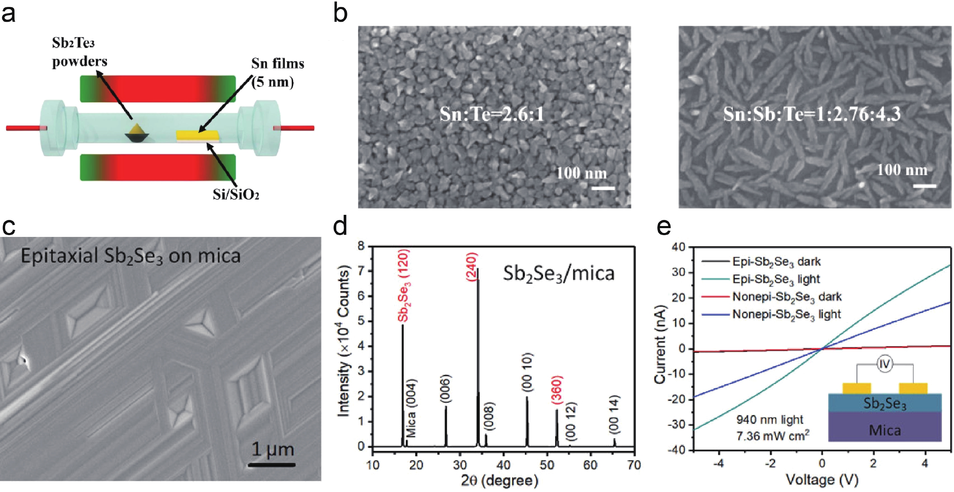
Wen X, Lu Z, Valdman L, et al. High-crystallinity epitaxial Sb 2Se 3 thin films on mica for flexible near-infrared photodetectors. ACS Appl Mater Interfaces, 2020, 12(31), 35222 doi: 10.1021/acsami.0c08467 |
| [45] |
An S, Liao Y, Kim M. Flexible titanium nitride/germanium-tin photodetectors based on sub-bandgap absorption. ACS Appl Mater Interfaces, 2021, 13(51), 61396 doi: 10.1021/acsami.1c15181 |
| [46] |
Woo S, Ryu G, Kang S S, et al. High-performance flexible InAs thin-film photodetector arrays with heteroepitaxial growth using an abruptly graded In xAl 1–xAs buffer. ACS Appl Mater Interfaces, 2021, 13(46), 55648 doi: 10.1021/acsami.1c14687 |
| [47] |
Woo S, Yeon E, Chu R J, et al. Flexible p-i-n InAs thin-film photodetector with low dark current enabled by an InAlAs barrier. Opt Mater Express, 2022, 12(6), 2374 doi: 10.1364/OME.457345 |
| [48] |
|
| [49] |
Zhu D, Ji D, Li L, et al. Recent progress in polymer-based infrared photodetectors. J Mater Chem C, 2022, 10(37), 13312 doi: 10.1039/D2TC00646D |
| [50] |
Ge Z, Xu N, Zhu Y, et al. Visible to mid-infrared photodetection based on flexible 3D graphene/organic hybrid photodetector with ultrahigh responsivity at ambient conditions. ACS Photonics, 2022, 9(1), 59 doi: 10.1021/acsphotonics.1c01690 |
| [51] |
Xu X, Chueh C C, Jing P, et al. High-performance near-IR photodetector using low-bandgap MA 0.5FA 0.5Pb 0.5Sn 0.5I 3 perovskite. Adv Funct Mater, 2017, 27(28), 1701053 doi: 10.1002/adfm.201701053 |
| [52] |
Dou L, Liu Y, Hong Z, et al. Low-bandgap near-IR conjugated polymers/molecules for organic electronics. Chem Rev, 2015, 115(23), 12633 doi: 10.1021/acs.chemrev.5b00165 |
| [53] |
Liu C, Wang K, Gong X, et al. Low bandgap semiconducting polymers for polymeric photovoltaics. Chem Soc Rev, 2016, 45(17), 4825 doi: 10.1039/C5CS00650C |
| [54] |
Simone G, Dyson M J, Meskers S C J, et al. Organic photodetectors and their application in large area and flexible image sensors: the role of dark current. Adv Funct Mater, 2020, 30(20), 1904205 doi: 10.1002/adfm.201904205 |
| [55] |
Dahiya H, Agrawal A, Sharma G D, et al. Organic bulk heterojunction enabled with nanocapsules of hydrate vanadium pentaoxide layer for high responsivity self−powered photodetector. J Semicond, 2022, 43(9), 092302 doi: 10.1088/1674-4926/43/9/092302 |
| [56] |
Siegmund B, Mischok A, Benduhn J, et al. Organic narrowband near-infrared photodetectors based on intermolecular charge−transfer absorption. Nat Commun, 2017, 8, 15421 doi: 10.1038/ncomms15421 |
| [57] |
Xiang H, Hu Z, Billot L, et al. Heavy-metal-free flexible hybrid polymer-nanocrystal photodetectors sensitive to 1.5 µm wavelength. ACS Appl Mater Interfaces, 2019, 11(45), 42571 doi: 10.1021/acsami.9b14034 |
| [58] |
Lv L, Dang W, Wu X, et al. Flexible short-wave infrared image sensors enabled by high-performance polymeric photodetectors. Macromolecules, 1063, 53(23), 10636 doi: 10.1021/acs.macromol.0c01988 |
| [59] |
Cho S, Yang Y, Soljačić M, et al. Submicrometer perovskite plasmonic lasers at room temperature. Sci Adv, 2021, 7(35), eabf3362 doi: 10.1126/sciadv.abf3362 |
| [60] |
Guo J, Liu T, Li M, et al. Ultrashort laser pulse doubling by metal-halide perovskite multiple quantum wells. Nat Commun, 2020, 11(1), 3361 doi: 10.1038/s41467-020-17096-6 |
| [61] |
Li Y, Zhou H, Xia M, et al. Phase-pure 2D tin halide perovskite thin flakes for stable lasing. Sci Adv, 2023, 9(32), eadh0517 doi: 10.1126/sciadv.adh0517 |
| [62] |
Jiang Q, Zhu K. Rapid advances enabling high-performance inverted perovskite solar cells. Nat Rev Mater, 2024, 9(6), 399 doi: 10.1038/s41578-024-00678-x |
| [63] |
Lin R, Wang Y, Lu Q, et al. All-perovskite tandem solar cells with 3D/3D bilayer perovskite heterojunction. Nature, 2023, 620(7976), 994 doi: 10.1038/s41586-023-06278-z |
| [64] |
Liu C, Yang Y, Chen H, et al. Two-dimensional perovskitoids enhance stability in perovskite solar cells. Nature, 2024633, 359 doi: 10.1038/s41586-024-07764-8 |
| [65] |
Kong L, Sun Y, Zhao B, et al. Fabrication of red-emitting perovskite LEDs by stabilizing their octahedral structure. Nature, 2024, 631(8019), 73 doi: 10.1038/s41586-024-07531-9 |
| [66] |
Li H, Zhu X, Zhang D, et al. Thermal management towards ultra-bright and stable perovskite nanocrystal-based pure red light-emitting diodes. Nat Commun, 2024, 15(1), 6561 doi: 10.1038/s41467-024-50634-0 |
| [67] |
Ooi Z Y, Jiménez S A, Gałkowski K, et al. Strong angular and spectral narrowing of electroluminescence in an integrated Tamm-plasmon-driven halide perovskite LED. Nat Commun, 2024, 15(1), 5802 doi: 10.1038/s41467-024-49838-1 |
| [68] |
Wang Y K, Jia F, Li X, et al. Self-assembled monolayer-based blue perovskite LEDs. Sci Adv, 2023, 9(36), eadh2140 doi: 10.1126/sciadv.adh2140 |
| [69] |
Pecunia V, Yuan Y, Zhao J, et al. Perovskite-inspired lead-free Ag 2BiI 5 for self−powered NIR-blind visible light photodetection. Nanomicro Lett, 2020, 12(1), 27 doi: 10.1007/s40820-020-0371-0 |
| [70] |
Mei L, Huang R, Shen C, et al. Hybrid halide perovskite-based near-infrared photodetectors and imaging arrays. Adv Optical Mater, 2022, 10(9), 2102656 doi: 10.1002/adom.202102656 |
| [71] |
Hu X, Wu J, Wu M, et al. Recent developments of infrared photodetectors with low-dimensional inorganic nanostructures. Nano Res, 2022, 15(2), 805 doi: 10.1007/s12274-021-3634-2 |
| [72] |
Guo H, Qi W. New materials and designs for 2D-based infrared photodetectors. Nano Res, 2023, 16(2), 3074 doi: 10.1007/s12274-022-4971-5 |
| [73] |
Liu C, Guo J, Yu L, et al. Silicon/2D-material photodetectors: from near-infrared to mid-infrared. Light Sci Appl, 2021, 10(1), 123 doi: 10.1038/s41377-021-00551-4 |
| [74] |
Du L, Wang C, Fang J, et al. A ternary SnS 1.26Se 0.76 alloy for flexible broadband photodetectors. RSC Adv, 2019, 9(25), 14352 doi: 10.1039/C9RA01734H |
| [75] |
Liu J, Li X, Wang H, et al. Ultrathin high−quality SnTe nanoplates for fabricating flexible near-infrared photodetectors. ACS Appl Mater Interfaces, 2020, 12(28), 31810 doi: 10.1021/acsami.0c07847 |
| [76] |
Liu J. L, Wang H, Li X, et al. Ultrasensitive flexible near-infrared photodetectors based on Van der Waals Bi 2Te 3 nanoplates. Appl Surf Sci, 2019, 484, 542 doi: 10.1016/j.apsusc.2019.03.295 |
| [77] |
Gupta N, Wang S, Higashitarumizu N, et al. Large-scale efficient mid-wave infrared optoelectronics based on black phosphorus ink. Sci Adv, 2023, 9(49), eadi9384 doi: 10.1126/sciadv.adi9384 |
| [78] |
Wang S, Wang G, Zhang Z, et al. Paper-based MoS 2/Bi 2S 3 heterojunction photodetectors for broadband detection and fast response. Mater Res Bull, 2024, 171, 112606 doi: 10.1016/j.materresbull.2023.112606 |
| [79] |
Long M, Gao A, Wang P, et al. Room temperature high-detectivity mid-infrared photodetectors based on black arsenic phosphorus. Sci Adv, 2017, 3(6), e1700589 doi: 10.1126/sciadv.1700589 |
| [80] |
Tong L, Huang X, Wang P, et al. Stable mid-infrared polarization imaging based on quasi-2D tellurium at room temperature. Nat Commun, 2020, 11(1), 2308 doi: 10.1038/s41467-020-16125-8 |
| [81] |
Li J, Niu L, Zheng Z, et al. Photosensitive graphene transistors. Adv Mater, 2014, 26(31), 5239 doi: 10.1002/adma.201400349 |
| [82] |
Li M, Yin B, Gao C, et al. Graphene: Preparation, tailoring, and modification. Exploration, 2023, 3(1), 20210233 doi: 10.1002/EXP.20210233 |
| [83] |
Xu H, Hao L, Liu H, et al. Flexible SnSe photodetectors with ultrabroad spectral response up to 10.6 µm enabled by photobolometric effect. ACS Appl Mater Interfaces, 2020, 12, 35250 doi: 10.1021/acsami.0c09561 |
| [84] |
Velusamy D B, Kim R. H, Cha S, et al. Flexible transition metal dichalcogenide nanosheets for band−selective photodetection. Nat Commun, 2015, 6, 8063 doi: 10.1038/ncomms9063 |
| [85] |
Ye Z, Tan C, Huang X, et al. Emerging MoS 2 wafer-scale technique for integrated circuits. Nanomicro Lett, 2023, 15(1), 38 doi: 10.1007/s40820-022-01010-4 |
| [86] |
Wang Y, Jiang K, Du J, et al. Green and near-infrared dual-mode afterglow of carbon dots and their applications for confidential information readout. Nanomicro Lett, 2021, 13(1), 198 doi: 10.1007/s40820-021-00718-z |
| [87] |
Wang Z, Gu Y, Li X, et al. Recent progress of quantum dot infrared photodetectors. Adv Optical Mater, 2023, 11(19), 2300970 doi: 10.1002/adom.202300970 |
| [88] |
Liu J, Liu P, Shi T, et al. Flexible and broadband colloidal quantum dots photodiode array for pixel-level X-ray to near-infrared image fusion. Nat Commun, 2023, 14(1), 5352 doi: 10.1038/s41467-023-40620-3 |
| [89] |
|
| [90] |
Zhou W, Shang Y, García A F P, et al. Solution-processed upconversion photodetectors based on quantum dots. Nat Electron, 2020, 3(5), 251 doi: 10.1038/s41928-020-0388-x |
| [91] |
Sa Z, Liu F, Liu D, et al. Ag-catalyzed GaSb nanowires for flexible near-infrared photodetectors. J Semicond, 2022, 43(11), 112302 doi: 10.1088/1674-4926/43/11/112302 |
| [92] |
Wang W, Lu X, Li Z, et al. Weak-acceptor-polyacrylonitrile/ donor-polyaniline core-shell nanofibers: A novel 1D polymeric heterojunction with high photoconductive properties. Org Electron, 2012, 13(11), 2319 doi: 10.1016/j.orgel.2012.06.033 |
| [93] |
Ran W, Wang L, Zhao S, et al. An integrated flexible all-nanowire infrared sensing system with record photosensitivity. Adv Mater, 2020, 32(16), 1908419 doi: 10.1002/adma.201908419 |
| [94] |
Meng Y, Li X, Kang X, et al. Van der Waals nanomesh electronics on arbitrary surfaces. Nat Commun, 2023, 14(1), 2431 doi: 10.1038/s41467-023-38090-8 |
| [95] |
Liu X, Ji X, Liu M, et al. High-performance Ge quantum dot decorated graphene/zinc-oxide heterostructure infrared photodetector. ACS Appl Mater Interfaces, 2015, 7(4), 2452 doi: 10.1021/am5072173 |
| [96] |
Mukherjee S, Jana S, Sinha T K, et al. Infrared tunable, two colour-band photodetectors on flexible platforms using 0D/2D PbS-MoS 2 hybrids. Nanoscale Adv, 2019, 1(8), 3279 doi: 10.1039/C9NA00302A |
| [97] |
Zhao X, Song L, Zhao R, et al. High-performance and flexible shortwave infrared photodetectors using composites of rare earth−doped nanoparticles. ACS Appl Mater Interfaces, 2019, 11(2), 2344 doi: 10.1021/acsami.8b16978 |
| [98] |
Shen C, Zhan W, Li M, et al. Development of in situ characterization techniques in molecular beam epitaxy. J Semicond, 2024, 45(3), 031301 doi: 10.1088/1674-4926/45/3/031301 |
| [99] |
Pan W, Zhang Z, Gu R, et al. Van der Waals epitaxy of HgCdTe thin films for flexible infrared optoelectronics. Adv Mater Interfaces, 2023, 10(4), 2201932 doi: 10.1002/admi.202201932 |
| [100] |
Yang Q, Wang X, He Z, et al. A centimeter-scale type-II weyl semimetal for flexible and fast ultra-broadband photodetection from ultraviolet to sub−millimeter wave regime. Adv Sci, 2023, 10(17), 2205609 doi: 10.1002/advs.202205609 |
| [101] |
Lei Y, Luo J, Yang X, et al. Thermal evaporation of large-area SnS 2 thin films with a UV-to-NIR photoelectric response for flexible photodetector applications. ACS Appl Mater Interfaces, 2020, 12(22), 24940 doi: 10.1021/acsami.0c01781 |
| [102] |
Yu H, Xie Y, Wei J, et al. Highly-bendable MoS 2/SnS flexible photodetector with broadband infrared response. Adv Mater Interfaces, 2022, 9(25), 2200896 doi: 10.1002/admi.202200896 |
| [103] |
Zhou H, Liu S, Yang M, et al. Flexible Sb 0.405Te 0.595 photodetectors with broadband spectral response up to 4.5 µm. Acta Mater, 2022, 226, 117631 doi: 10.1016/j.actamat.2022.117631 |
| [104] |
Wang Y, Zhang T, Samigullina D, et al. Semitransparent near-infrared organic photodetectors: flexible, large-area, and physical-vapor-deposited for versatile advanced optical applications. Adv Funct Mater, 2024, 34(23), 2313689 doi: 10.1002/adfm.202313689 |
| [105] |
Zhou Q, Lu D, Tang H, et al. Self-powered ultra-broadband and flexible photodetectors based on the bismuth films by vapor deposition. ACS Appl Electron Mater, 2020, 2(5), 1254 doi: 10.1021/acsaelm.0c00058 |
| [106] |
Li D, Yip S, Li F, et al. Flexible near-infrared InGaSb nanowire array detectors with ultrafast photoconductive response below 20 µs. Adv Optical Mater, 2020, 8(22), 2001201 doi: 10.1002/adom.202001201 |
| [107] |
Yin Y, Guo Y, Liu D, et al. Substrate-free chemical vapor deposition of large-scale III-V nanowires for high-performance transistors and broad-spectrum photodetectors. Adv Optical Mater, 2022, 10(6), 2102291 doi: 10.1002/adom.202102291 |
| [108] |
Choi J M, Jang H Y, Kim A R, et al. Ultra-flexible and rollable 2D-MoS 2/Si heterojunction-based near-infrared photodetector via direct synthesis. Nanoscale, 2021, 13(2), 672 doi: 10.1039/D0NR07091B |
| [109] |
Hoang A T, Hu L, Kim B J, et al. Low-temperature growth of MoS 2 on polymer and thin glass substrates for flexible electronics. Nat Nanotechnol, 2023, 18(12), 1439 doi: 10.1038/s41565-023-01460-w |
| [110] |
Lee W Y, Ha S, Lee H, et al. High-detectivity flexible near-infrared photodetector based on chalcogenide Ag 2Se nanoparticles. Adv Optical Mater, 2019, 7(22), 1900812 doi: 10.1002/adom.201900812 |
| [111] |
Hu J, Yang S, Zhang Z, et al. Solution-processed, flexible and broadband photodetector based on CsPbBr 3/PbSe quantum dot heterostructures. J Mater Sci Technol, 2021, 68, 216 doi: 10.1016/j.jmst.2020.06.047 |
| [112] |
Peng M, Wang Y, Shen Q, et al. High-performance flexible and broadband photodetectors based on PbS quantum dots/ZnO nanoparticles heterostructure. Sci China Mater, 2019, 62(2), 225 doi: 10.1007/s40843-018-9311-9 |
| [113] |
Akhavan S, Ruocco A, Soavi G, et al. Graphene-black phosphorus printed photodetectors. 2D Mater, 2023, 10(3), 035015 doi: 10.1088/2053-1583/acc74c |
| [114] |
Wang J, Pan Q, Xie H, et al. Printed chalcogenide/metal heterostructured photodetectors for flexible near-infrared sensing. Adv Optical Mater, 2022, 10(13), 2200173 doi: 10.1002/adom.202200173 |
| [115] |
Shi B, Wang P, Feng J, et al. Split-ring structured all-inorganic perovskite photodetector arrays for masterly internet of things. Nanomicro Lett, 2022, 15(1), 3 doi: 10.1007/s40820-022-00961-y |
| [116] |
Thabit M Y H, Kaawash N M S, Halge D I, et al. Flexible infrared photodetector based on polyethylene terephthalate (PET) supported lead sulfide thin film. Physica B, 2023, 669, 415314 doi: 10.1016/j.physb.2023.415314 |
| [117] |
Li L, Ye G, Luo T, et al. Centimeter-sized stable zero-dimensional Cs 3Bi 2I 9 single crystal for mid-infrared lead-free perovskite photodetector. J Phys Chem C, 2022, 126(7), 3646 doi: 10.1021/acs.jpcc.1c08815 |
| [118] |
Xia Y, Geng C, Bi X, et al. Biomimetic flexible high-sensitivity near-infrared II organic photodetector for photon detection and imaging. Adv Optical Mater, 2024, 12(3), 2301518 doi: 10.1002/adom.202301518 |
| [119] |
Feng X, He Y, Qu W, et al. Spray-coated perovskite hemispherical photodetector featuring narrow-band and wide-angle imaging. Nat Commun, 2022, 13(1), 6106 doi: 10.1038/s41467-022-33934-1 |
| [120] |
Zhang K, Wang Y, Wang H, et al. Sulfur-passivated InSb nanowires for infrared photodetectors. ACS Appl Nano Mater, 2023, 6(8), 6810 doi: 10.1021/acsanm.3c00519 |
| [121] |
Huang Z, Gao M, Pan T, et al. Interface engineered carbon nanotubes with SiO 2 for flexible infrared detectors. Appl Surf Sci, 2017, 413, 308 doi: 10.1016/j.apsusc.2017.04.059 |
| [122] |
Jang W, Rehman Z U, Haris M, et al. Oxide vacancy passivation through interface engineering of tetraphenylethylene-based small-molecule with sulfonate functional group for efficient organic photodetector. Chem Eng J, 2023, 472, 144847 doi: 10.1016/j.cej.2023.144847 |
| [123] |
Liu Y, Hu H, Yuan M, et al. Red-sensitive image array based on defect-engineered PBDB-T/WSe 1.5-WSe 2/graphene heterostructure. Adv Electron Mater, 2023, 9(7), 2300115 doi: 10.1002/aelm.202300115 |
| [124] |
Hu C, Chai R, Wei Z, et al. ZnSb/Ti 3C 2T x MXene van der Waals heterojunction for flexible near-infrared photodetector arrays. J Semicond, 2024, 45(5), 052601 doi: 10.1088/1674-4926/45/5/052601 |
| [125] |
Zhang Z, Ji P, Li S, et al. High-performance broadband flexible photodetector based on Gd 3Fe 5O 12-assisted double van der Waals heterojunctions. Microsyst Nanoeng, 2023, 9(1), 84 doi: 10.1038/s41378-023-00548-6 |
| [126] |
Su W, Zhang S, Liu C, et al. Interlayer transition induced infrared response in ReS 2/2D perovskite van der Waals heterostructure photodetector. Nano Lett, 2022, 22(24), 10192 doi: 10.1021/acs.nanolett.2c04328 |
| [127] |
Zheng T, Yang M, Pan Y, et al. Self-powered pphotodetector with high efficiency and polarization sensitivity enabled by WSe 2/Ta 2NiSe 5/WSe 2 van der Waals dual heterojunction. ACS Appl Mater Interfaces, 2023, 15(24), 29363 doi: 10.1021/acsami.3c04147 |
| [128] |
Sahatiya P, Reddy K C S, Badhulika S. Discretely distributed 1D V 2O 5 nanowires over 2D MoS 2 nanoflakes for an enhanced broadband flexible photodetector covering the ultraviolet to near infrared region. J Mater Chem C, 2017, 5(48), 12728 doi: 10.1039/C7TC05036D |
| [129] |
Park S, Fukuda K, Wang M, et al. Ultraflexible near-infrared organic photodetectors for conformal photoplethysmogram sensors. Adv Mater, 2018, 30(34), 1802359 doi: 10.1002/adma.201802359 |
| [130] |
Wang C, Xiao M, Qiao J, et al. High stability of dark current enables stretchable near-infrared self-powered organic photodetectors. Appl Phys Lett, 2024, 124(18), 183301 doi: 10.1063/5.0202910 |
| [131] |
Yu W, Li S, Zhang Y, et al. Near-infrared photodetectors based on MoTe 2/graphene heterostructure with high responsivity and flexibility. Small, 2017, 13(24), 1700268 doi: 10.1002/smll.201700268 |
| [132] |
Shafa M, Wu D, Chen X, et al. Flexible infrared photodetector based on indium antimonide nanowire arrays. Nanotechnology, 2021, 32(27), 27LT01 doi: 10.1088/1361-6528/abe965 |
| [133] |
Tao Y, Wu X, Wang W, et al. Flexible photodetector from ultraviolet to near infrared based on a SnS 2 nanosheet microsphere film. J Mater Chem C, 2015, 3(6), 1347 doi: 10.1039/C4TC02325K |
| [134] |
Ji Y, Zhou D, Wang N, et al. Flexible double narrowband near-infrared photodetector based on PMMA/core-shell upconversion nanoparticle composites. J Rare Earths, 2022, 40(2), 211 doi: 10.1016/j.jre.2020.12.001 |
| [135] |
Liu S, Huang Z, Qiao H, et al. Two-dimensional Bi 2Se 3 nanosheet based flexible infrared photodetector with pencil-drawn graphite electrodes on paper. Nanoscale, Adv, 2020, 2(2), 906 doi: 10.1039/C9NA00745H |
| [136] |
Sun H, Lei T, Tian W, et al. Self-powered, flexible, and dolution-processable perovskite photodetector based on low-cost carbon cloth. Small, 2017, 13(28), 1701042 doi: 10.1002/smll.201701042 |
| [137] |
Tsai S Y, Lin C C, Yu C T, et al. Screen-printable silver paste material for semitransparent and flexible metal-semiconductor-metal photodetectors with liquid-phase procedure. Nanomaterials, 2022, 12(24), 2428 doi: 10.3390/nano12142428 |
| [138] |
Sheng L, Yi C, Zheng L, et al. Solution-processed broadband photodetectors without transparent conductive oxide electrodes. J Mater Chem C, 2022, 10(7), 2783 doi: 10.1039/D1TC04278E |
| [139] |
Bai S, Zhang S, Zhou W, et al. Laser-assisted reduction of highly conductive circuits based on copper nitrate for flexible printed sensors. Nanomicro Lett, 2017, 9(4), 42 doi: 10.1007/s40820-017-0139-3 |
| [140] |
Lei Y, Gu L, Yang X, et al. Ductile-metal Ag as buffer layer for flexible self-powered Ag 2S photodetectors. Adv Mater Interfaces, 2021, 8(9), 2002255 doi: 10.1002/admi.202002255 |
| [141] |
Hu C, Li L, Shen G. Flexible transparent near-infrared photodetector based on 2D TiC MXene-Te van Der Waals heterostructures†. Chin J Chem, 2021, 39(8), 2141 doi: 10.1002/cjoc.202100229 |
| [142] |
Wang Z, Shen G. Flexible optoelectronic sensors: status and prospects. Mater Chem Front, 2023, 7(8), 1496 doi: 10.1039/D2QM01319C |
| [143] |
Liang Y, Ding Q, Wang H, et al. Humidity sensing of stretchable and transparent hydrogel films for wireless respiration monitoring. Nanomicro Lett, 2022, 14(1), 183 doi: 10.1007/s40820-022-00934-1 |
| [144] |
Chang S, Koo J H, Yoo J, et al. Flexible and stretchable light-emitting diodes and photodetectors for human-centric optoelectronics. Chem Rev, 2024, 124(3), 768 doi: 10.1021/acs.chemrev.3c00548 |
| [145] |
Li H, Ma Y, Huang Y. Material innovation and mechanics design for substrates and encapsulation of flexible electronics: A review. Mater Horiz, 2021, 8(2), 383 doi: 10.1039/D0MH00483A |
| [146] |
Zhang Y, Yan Z, Nan K, et al. A mechanically driven form of Kirigami as a route to 3D mesostructures in micro/nanomembranes. Proc Natl Acad Sci USA, 2015, 112(38), 11757 doi: 10.1073/pnas.1515602112 |
| [147] |
Zhao J, Zhang C, Zou D, et al. A structured design for highly stretchable rlectronic dkin. Adv Mater Technol, 2019, 4(10), 1900492 doi: 10.1002/admt.201900492 |
| [148] |
Morikawa Y, Yamagiwa S, Sawahata H, et al. Ultrastretchable kirigami bioprobes. Adv Healthcare Mater, 2018, 7(3), 1701100 doi: 10.1002/adhm.201701100 |
| [149] |
Qiu Y, Zhang B, Yang J, et al. Wafer-scale integration of stretchable semiconducting polymer microstructures via capillary gradient. Nat Commun, 2021, 12(1), 7038 doi: 10.1038/s41467-021-27370-w |
| [150] |
Ko H C, Stoykovich M P, Song J, et al. A hemispherical electronic eye camera based on compressible silicon optoelectronics. Nature, 2008, 454(7205), 748 doi: 10.1038/nature07113 |
| [151] |
Kim D. W, Kong M, Jeong U. Interface design for stretchable electronic devices. Adv Sci, 2021, 8(8), 2004170 doi: 10.1002/advs.202004170 |
| [152] |
Lee J, Wu J, Shi M, et al. Stretchable GaAs photovoltaics with designs that enable high areal coverage. Adv Mater, 2011, 23(8), 986 doi: 10.1002/adma.201003961 |
| [153] |
Tang Y, Lin G, Han L, et al. Design of hierarchically cut hinges for highly stretchable and reconfigurable metamaterials with enhanced strength. Adv Mater, 2015, 27(44), 7181 doi: 10.1002/adma.201502559 |
| [154] |
Gu M, Song W J, Hong J, et al. Stretchable batteries with gradient multilayer conductors. Sci Adv, 2019, 5(7), eaaw1879 doi: 10.1126/sciadv.aaw1879 |
| [155] |
Zhuang Q, Yao K, Zhang C, et al. Permeable, three-dimensional integrated electronic skins with stretchable hybrid liquid metal solders. Nat Electron, 2024, 7(7), 598 doi: 10.1038/s41928-024-01189-x |
| [156] |
Wang X, Dong S, Huang S, et al. Near-infrared InGaAs intelligent spectral sensor by 3D heterogeneous hybrid integration. Adv Photonics Res, 2023, 4(8), 2300043 doi: 10.1002/adpr.202300043 |
| [157] |
Hua Q, Shen G. Low−dimensional nanostructures for monolithic 3D-integrated flexible and stretchable electronics. Chem Soc Rev, 2024, 53(3), 1316 doi: 10.1039/D3CS00918A |
| [158] |
Kang J H, Shin H, Kim K S, et al. Monolithic 3D integration of 2D materials-based electronics towards ultimate edge computing solutions. Nat Mater, 2023, 22(12), 1470 doi: 10.1038/s41563-023-01704-z |
| [159] |
Wang H, Zhen H L, Li S L, et al. Self-rolling and light-trapping in flexible quantum well-embedded nanomembranes for wide-angle infrared photodetectors. Sci Adv, 2016, 2(8), e1600027 doi: 10.1126/sciadv.1600027 |
| [160] |
Zhu Y, Geng C, Hu L G, et al. Skin-like near-infrared II photodetector with high performance for optical communication, imaging, and proximity sensing. Chem Mater, 2023, 35(5), 2114 doi: 10.1021/acs.chemmater.2c03701 |
| [161] |
Shen Y C, Lee C Y, Wang H H, et al. Embedded integration of Sb 2Se 3 film by low-temperature plasma-assisted chemical vapor reaction with polycrystalline Si transistor for high-performance flexible visible-to-near-infrared photodetector. ACS Nano, 2023, 17(3), 2019 doi: 10.1021/acsnano.2c07288 |
| [162] |
Kim J, Kwon S M, Kang Y. K, et al. A skin-like two-dimensionally pixelized full-color quantum dot photodetector. Sci Adv, 2019, 5(11), eaax8801 doi: 10.1126/sciadv.aax8801 |
| [163] |
Degenstein L M, Sameoto D, Hogan J D, et al. Smart textiles for visible and IR camouflage application: state-of-the-art and microfabrication path forward. Micromachines, 2021, 12(7), 773 doi: 10.3390/mi12070773 |
| [164] |
Tian T, Wei X, Elhassan A, et al. Highly flexible, efficient, and wearable infrared radiation heating carbon fabric. Chem Eng J, 2021, 417, 128114 doi: 10.1016/j.cej.2020.128114 |
| [165] |
Simões J, Dong T, Yang Z. Non−fullerene acceptor organic photodetector for skin−conformable photoplethysmography applications. Adv Mater Interfaces, 2022, 9(10), 2101897 doi: 10.1002/admi.202101897 |
| [166] |
Xin Q, Ma H, Wang H, et al. Tracking tumor heterogeneity and progression with near-infrared II fluorophores. Exploration, 2023, 3(2), 2022001 doi: 10.1002/exp.20220011 |
| [167] |
Ollearo R, Ma X, Akkerman H B, et al. Vitality surveillance at distance using thin-film tandem-like narrowband near-infrared photodiodes with light-enhanced responsivity. Sci Adv, 2023, 9(7), eadf9861 doi: 10.1126/sciadv.adf9861 |
| [168] |
Liu S, Wang X, Xu N, et al. A flexible and wearable photodetector enabling ultra-broadband imaging from ultraviolet to millimeter-mave regimes. Adv Sci, 2024, 11(26), 2401631 doi: 10.1002/advs.202401631 |
| [169] |
Kim T H, Zhou Z, Choi Y S, et al. Flexible biomimetic block copolymer composite for temperature and long-wave infrared sensing. Sci Adv, 2023, 9(6), eade0423 doi: 10.1126/sciadv.ade0423 |
| [170] |
Hao Q, Tang X, Cheng Y, et al. Development of flexible and curved infrared detectors with HgTe colloidal quantum dots. Infrared Phys Technol, 2020, 108, 103344 doi: 10.1016/j.infrared.2020.103344 |
| [171] |
He Z P, Han X, Wu W Q, et al. Recent advances in bioinspired vision systems with curved imaging structures. Rare Met, 2024, 43(4), 1407 doi: 10.1007/s12598-023-02573-w |
| [172] |
Ding Y, Liu G, Long Z, et al. Uncooled self-powered hemispherical biomimetic pit organ for mid- to long-infrared imaging. Sci Adv, 2022, 8(35), eabq8432 doi: 10.1126/sciadv.abq8432 |
| [173] |
Tang X, Ackerman M M, Shen G, et al. Towards infrared electronic eyes: flexible colloidal quantum dot photovoltaic detectors enhanced by resonant cavity. Small, 2019, 15(12), 1804920 doi: 10.1002/smll.201804920 |
| [174] |
Gao W, Xu Z, Han X, et al. Recent advances in curved image sensor arrays for bioinspired vision system. Nano Today, 2022, 42, 101366 doi: 10.1016/j.nantod.2021.101366 |
| [175] |
Choi C, Choi M K, Liu S, et al. Human eye-inspired soft optoelectronic device using high-density MoS 2-graphene curved image sensor array. Nat Commun, 2017, 8, 1664 doi: 10.1038/s41467-017-01824-6 |
| [176] |
Jung I, Xiao J, Malyarchuk V, et al. Dynamically tunable hemispherical electronic eye camera system with adjustable zoom capability. Proc Natl Acad Sci USA, 2011, 108(5), 1788 doi: 10.1073/pnas.1015440108 |
| [177] |
Lee E K, Baruah R K, Leem J W, et al. Fractal web design of a hemispherical photodetector array with organic-dye-sensitized graphene hybrid composites. Adv Mater, 2020, 32(46), 2004456 doi: 10.1002/adma.202004456 |
| [178] |
Gu L, Poddar S, Lin Y, et al. A biomimetic eye with a hemispherical perovskite nanowire array retina. Nature, 2020, 581(7808), 278 doi: 10.1038/s41586-020-2285-x |
| [179] |
Yang X. Enhanced performance of near-infrared- photodetector with PbS-QD-sensitised field-effect transistor. Opt Mater, 2024, 154, 115634 doi: 10.1016/j.optmat.2024.115634 |
| [180] |
Long Z, Ding Y, Qiu X, et al. A dual-mode image sensor using an all−inorganic perovskite nanowire array for standard and neuromorphic imaging. J Semicond, 2023, 44(9), 092604 doi: 10.1088/1674-4926/44/9/092604 |
| [181] |
Tian B, Xie Z, Chen L, et al. Ultralow-power in-memory computing based on ferroelectric memcapacitor network. Exploration, 2023, 3(3), 20220126 doi: 10.1002/EXP.20220126 |
| [182] |
Wu G, Zhang X, Feng G, et al. Ferroelectric-defined reconfigurable homojunctions for in-memory sensing and computing. Nat Mater, 2023, 22, 1499 doi: 10.1038/s41563-023-01676-0 |
| [183] |
Zhou G, Li J, Song Q, et al. Full hardware implementation of neuromorphic visual system based on multimodal optoelectronic resistive memory arrays for versatile image processing. Nat Commun, 2023, 14(1), 8489 doi: 10.1038/s41467-023-43944-2 |
| [184] |
Cai Y, Jiang Y, Sheng C, et al. In-situ artificial retina with all-in-one reconfigurable photomemristor networks. NPJ Flex Electron, 2023, 7(1), 29 doi: 10.1038/s41528-023-00262-3 |
| [185] |
Yu R, He L, Gao C, et al. Programmable ferroelectric bionic vision hardware with selective attention for high-precision image classification. Nat Commun, 2022, 13(1), 7019 doi: 10.1038/s41467-022-34565-2 |
| [186] |
Liu Q, Wei Q, Ren H, et al. Circular polarization-resolved ultraviolet photonic artificial synapse based on chiral perovskite. Nat Commun, 2023, 14(1), 7179 doi: 10.1038/s41467-023-43034-3 |
| [187] |
Wang Y, Zha Y, Bao C, et al. Monolithic 2D perovskites enabled artificial photonic synapses for neuromorphic vision sensors. Adv Mater, 2024, 36(18), 2311524 doi: 10.1002/adma.202311524 |
| [188] |
Hong S, Cho H, Kang B. H, et al. Neuromorphic active pixel image sensor array for visual memory. ACS Nano, 2021, 15(9), 15362 doi: 10.1021/acsnano.1c06758 |
| [189] |
Han C, Han J, He M, et al. Photonic synaptic transistor with memory mode switching for neuromorphic visual system. Laser Photonics Rev, 2024, 18(7), 2300976 doi: 10.1002/lpor.202300976 |
| [190] |
Xie Y, Yu H, Wei J, et al. Bending strain-modulated flexible photodetection of tellurene in the long wavelength infrared region. J Alloys Compd, 2023, 968, 171899 doi: 10.1016/j.jallcom.2023.171899 |
| [191] |
Pu K, Xu Z, Gao Y, et al. A flexible sensitive visible-NIR organic photodetector with high durability. Adv Mater Technol, 2023, 8(16), 2300207 doi: 10.1002/admt.202300207 |
| [192] |
Qin S, Du Q, Dong R, et al. Robust, flexible and broadband photodetectors based on van der Waals graphene/C 60 heterostructures. Carbon, 2020, 167, 668 doi: 10.1016/j.carbon.2020.06.056 |
| [193] |
Li W, Chen J, Lin H, et al. The UV-vis-NIR broadband ultrafast flexible Sn-Pb perovskite photodetector for multispectral imaging to distinguish substance and foreign-body in biological tissues. Adv Optical Mater, 2024, 12(2), 2301373 doi: 10.1002/adom.202301373 |
| [194] |
Xu X, Wang Y, Ji Y, et al. High-performance flexible broadband photoelectrochemical photodetector based on molybdenum telluride. Small, 2024, 20(27), 2308590. doi: 10.1002/smll.202308590 |
| [195] |
Zhang R, Yang Z, Liu, L, et al. Highly sensitive broadband bolometric photodetectors based on 2D PdSe 2 thin film. Adv Optical Mater, 2023, 11(23), 2301055 doi: 10.1002/adom.202301055 |
| [196] |
Zhang S, Zhang T, Liu Z, et al. Flexible and robust 3D a-SiGe radial junction near-infrared photodetectors for rapid sphygmic signal monitoring. Adv Funct Mater, 2022, 32(2), 2107040 doi: 10.1002/adfm.202107040 |
| [197] |
Yang H, Pan L, Wang X, et al. Mixed-valence-driven quasi-1D Sn IISn IVS 3 with highly polarization-sensitive UV-vis-NIR photoresponse. Adv Funct Mater, 2019, 29(38), 1904416 doi: 10.1002/adfm.201904416 |
| [198] |
Wu W, Wang Y, Niu Y, et al. Thermal localization enhanced fast photothermoelectric response in a quasi-one-dimensional flexible NbS 3 photodetector. ACS Appl Mater Interfaces, 2020, 12(12), 14165 doi: 10.1021/acsami.0c00764 |
| [199] |
Kwon J B, Kim S W, Kang B H, et al. Air-stable and ultrasensitive solution-cast SWIR photodetectors utilizing modified core/shell colloidal quantum dots. Nano Converg, 2020, 7(1), 28 doi: 10.1186/s40580-020-00238-3 |
| [200] |
Wu D, Du G, Liu H, et al. Flexible microcomb printed PbS quantum dot film enables scalable fabrication of near infrared photodetector. Adv Optical Mater, 2023, 11(23), 2300945 doi: 10.1002/adom.202300945 |


 Yegang Liang received his bachelor's degree in 2020 and his master's degree in 2023, both from Guangxi University. He is currently a doctoral student at Beijing Institute of Technology, focusing on the research of flexible and curved infrared sensors.
 Wenhao Ran received his PhD in the Institute of Semiconductors, Chinese Academy of Sciences in 2022. He is currently a postdoctoral researcher at the School of Integrated Circuits and Electronics, Beijing Institute of Technology, Beijing. His current research focuses on flexible biomimic vision system with in-memory sensing and computing.
 Dan Kuang received her doctoral degree from Beijing institute of technology, China, in 2023. She is currently an experimentalist with school of integrated circuits and electronics, Beijing institute of technology, China. Her current research focuses on semiconductor nanomaterials and flexible devices.
 Zhuoran Wang received his PhD in the Mining and Materials Engineering from McGill University, QC, Canada in 2017. In 2019 he joined the Institute of Photonic Sciences (ICFO), Barcelona, as a postdoctoral/Marie-Curie research fellow. He is currently a professor at the School of Integrated Circuits and Electronics, Beijing Institute of Technology, Beijing. His current research focuses on flexible optoelectronic sensors for biomimic vision.
 DownLoad: