| [1] |
Schroder D K. Semiconductor material and device characterization. Wiley, 2005, 12 doi: 10.1002/0471749095 |
| [2] |
Diasso A, Sam R, Zouma B, et al. Experimental measurement of minority carriers effective lifetime in silicon solar cell using open circuit voltage decay under magnetic field in transient mode. Smart Grid Renew Energy, 2020, 11(11), 181 doi: 10.4236/sgre.2020.1111011 |
| [3] |
Li X X, He J H. A simplified formulation for calculation of minority-carrier effective lifetime. Results Phys, 2018, 11, 623 doi: 10.1016/j.rinp.2018.10.008 |
| [4] |
Lemaire A, Perona A, Caussanel M, et al. Open-circuit voltage decay simulations on silicon and gallium arsenide p-n homojunctions: Design influences on bulk lifetime extraction. Microelectron J, 2020, 101, 104735 doi: 10.1016/j.mejo.2020.104735 |
| [5] |
Gossick B R. On the transient behavior of semiconductor rectifiers. J Appl Phys, 1955, 26(11), 1356 doi: 10.1063/1.1721908 |
| [6] |
Choo S C, Mazur R G. Open circuit voltage decay behavior of junction devices. Solid State Electron, 1970, 13(5), 553 doi: 10.1016/0038-1101(70)90136-X |
| [7] |
|
| [8] |
Davies L W. The use of P-L-N structures in investigations of transient recombination from high injection levels in semiconductors. Proc IEEE, 1963, 51(11), 1637 doi: 10.1109/PROC.1963.2639 |
| [9] |
Ko W H. The reverse transient behavior of semiconductor junction diodes. IRE Trans Electron Devices, 1961, 8(2), 123 doi: 10.1109/T-ED.1961.14719 |
| [10] |
Bassett R J, Eulop W, Hogarth C A. Determination of the bulk carrier lifetime in the low-doped region of a silicon power diode, by the method of open circuit voltage decay. Int J Electron, 1973, 35(2), 177 doi: 10.1080/00207217308938533 |
| [11] |
Bassett R J. Observations on a method of determining the carrier lifetime in p +-ν-n + diodes. Solid State Electron, 1969, 12(5), 385 doi: 10.1016/0038-1101(69)90094-X |
| [12] |
Davies L W. Electron-hole scattering at high injection-levels in germanium. Nature, 1962, 194, 762 doi: 10.1038/194762a0 |
| [13] |
Howard N R, Johnson G W. P + IN + silicon diodes at high forward current densities. Solid State Electron, 1965, 8(3), 275 doi: 10.1016/0038-1101(65)90143-7 |
| [14] |
Lindholm F A, Sah C T. Normal modes of semiconductor p-n–junction devices for material-parameter determination. J Appl Phys, 1976, 47(9), 4203 doi: 10.1063/1.323290 |
| [15] |
Liu S L, Fei G T, Xu S H, et al. High-performance visible-near IR photodetectors based on high-quality Sn 2+ -sensitized PbS films. J Alloys Compd, 2021, 883, 160860 doi: 10.1016/j.jallcom.2021.160860 |
| [16] |
Yin X T, Zhang C, Guo Y X, et al. PbS QD-based photodetectors: Future-oriented near-infrared detection technology. J Mater Chem C, 2021, 9(2), 417 doi: 10.1039/D0TC04612D |
| [17] |
Gao L F, Chen H L, Wang R, et al. Ultra-small 2D PbS nanoplatelets: Liquid-phase exfoliation and emerging applications for photo-electrochemical photodetectors. Small, 2021, 17(5), 2005913 doi: 10.1002/smll.202005913 |
| [18] |
Kumar S, Sharma T P, Zulfequar M, et al. Characterization of vacuum evaporated PbS thin films. Phys B: Condens Matter, 2003, 325, 8 doi: 10.1016/S0921-4526(02)01272-3 |
| [19] |
Williamson G K, Hall W H. X-ray line broadening from filed aluminium and wolfram. Acta Metall, 1953, 1(1), 22 doi: 10.1016/0001-6160(53)90006-6 |
| [20] |
Van T N, Laborde E, Champeaux C, et al. Tunability of optical properties of InSb films developed by pulsed laser deposition. Appl Surf Sci, 2023, 619, 156756 doi: 10.1016/j.apsusc.2023.156756 |
| [21] |
Nanda K K, Sahu S N, Soni R K, et al. Raman spectroscopy of PbS nanocrystalline semiconductors. Phys Rev B, 1998, 58(23), 15405 doi: 10.1103/PhysRevB.58.15405 |
| [22] |
Xiong S L, Xi B J, Xu D C, et al. L-cysteine-assisted tunable synthesis of PbS of various morphologies. J Phys Chem C, 2007, 111(45), 16761 doi: 10.1021/jp075096z |
| [23] |
Smith G D, Firth S, Clark R J H, et al. First- and second-order Raman spectra of galena (PbS). J Appl Phys, 2002, 92, 4375 doi: 10.1063/1.1505670 |
| [24] |
Krauss T D, Wise F W. Raman-scattering study of exciton-phonon coupling in PbS nanocrystals. Phys Rev B, 1997, 55(15), 9860 doi: 10.1103/PhysRevB.55.9860 |
| [25] |
Cao H Q, Wang G Z, Zhang S C, et al. Growth and photoluminescence properties of PbS nanocubes. Nanotechnology, 2006, 17(13), 3280 doi: 10.1088/0957-4484/17/13/034 |
| [26] |
Krauss T D, Wise F W, Tanner D B. Observation of coupled vibrational modes of a semiconductor nanocrystal. Phys Rev Lett, 1996, 76(8), 1376 doi: 10.1103/PhysRevLett.76.1376 |
| [27] |
Rivera-Nieblas J O, Alvarado-Rivera J, Acosta-Enríquez M C, et al. Resistance and resistivities of pbs thin films using polyethylenimine by chemical bath deposition. Chalcogenide Lett, 2013, 10, 349
|
| [28] |
|
| [29] |
Shahane G S, More B M, Rotti C B, et al. Studies on chemically deposited CdS 1−xSe x mixed thin films. Mater Chem Phys, 1997, 47(2/3), 263 doi: 10.1016/S0254-0584(97)80062-4 |
| [30] |
Lee W, Dasgupta N P, Jung H J, et al. Scanning tunneling spectroscopy of lead sulfide quantum wells fabricated by atomic layer deposition. Nanotechnology, 2010, 21(48), 485402 doi: 10.1088/0957-4484/21/48/485402 |
| [31] |
Ahrenkiel, Richard K, Lundstrom M S. Chapter 2 minority-carrier lifetime in III–V semiconductors ed. Academic Press Semiconductors and Semimetals, 1993, 39, 39 doi: 10.1016/S0080-8784(08)62594-6 |
| [32] |
Donahoe F J. Electronic semiconductors. J Frankl Inst, 1958, 266(5), 419
|
| [33] |
Connelly B C, Metcalfe G D, Shen H E, et al. Direct minority carrier lifetime measurements and recombination mechanisms in long-wave infrared type II superlattices using time-resolved photoluminescence. Appl Phys Lett, 2010, 97(25), 251117 doi: 10.1063/1.3529458 |
| [34] |
Keitel R C, Brechbühler R, Cocina A, et al. Fluctuations in the photoluminescence excitation spectra of individual semiconductor nanocrystals. J Phys Chem Lett, 2024, 15(18), 4844 doi: 10.1021/acs.jpclett.4c00516 |
| [35] |
Bhosale J S, Moore J E, Wang X, et al. Steady-state photoluminescent excitation characterization of semiconductor carrier recombination. Review of Scientific Instruments, 2016, 87(1), 013104 doi: 10.1063/1.4939047 |
| [36] |
Hariharan A, Schäfer S, Heise S J. Decay of excess carriers in a two-defect model semiconductor: A time-resolved photoluminescence study. J Appl Phys, 2021, 130(23), 235702 doi: 10.1063/5.0065600 |
| [37] |
Krückemeier L, Krogmeier B, Liu Z F, et al. Understanding transient photoluminescence in halide perovskite layer stacks and solar cells. Adv Energy Mater, 2021, 11(19), 2003489 doi: 10.1002/aenm.202003489 |
| [38] |
Endale G. Effects of transition energy on intra-band photoluminescence of zinc oxide (ZnO) semiconductor under low injection level. Ujms, 2019, 7(3), 35 doi: 10.13189/ujms.2019.070301 |
| [39] |
Semyonov O, Subashiev A V, Chen Z C, et al. Photon assisted Lévy flights of minority carriers in n-InP. J Lumin, 2012, 132(8), 1935 doi: 10.1016/j.jlumin.2012.03.035 |
| [40] |
Nguyen H T, Phang S P, Wong-Leung J, et al. Photoluminescence excitation spectroscopy of diffused layers on crystalline silicon wafers. IEEE J Photovolt, 2016, 6(3), 746 doi: 10.1109/JPHOTOV.2016.2532460 |
| [41] |
Kirchartz T, Márquez J A, Stolterfoht M, et al. Photoluminescence-based characterization of halide perovskites for photovoltaics. Adv Energy Mater, 2020, 10(26), 1904134 doi: 10.1002/aenm.201904134 |
| [42] |
Dev S, Wang Y N, Kim K, et al. Measurement of carrier lifetime in micron-scaled materials using resonant microwave circuits. Nat Commun, 2019, 10(1), 1625 doi: 10.1038/s41467-019-09602-2 |
| [43] |
Lemaire A, Perona A, Caussanel M, et al. Open-circuit voltage decay: Moving to a flexible method of characterisation. IET Circuits Devices Syst, 2020, 14(7), 947 doi: 10.1049/iet-cds.2020.0123 |
| [44] |
Sakata I, Hayashi Y. Open-circuit voltage decay (OCVD) measurement applied to hydrogenated amorphous silicon solar cells. Jpn J Appl Phys, 1990, 29(1A), L27 doi: 10.1143/JJAP.29.L27 |
| [45] |
Gupta G K, Garg A, Dixit A. Electrical and impedance spectroscopy analysis of Sol-gel derived spin coated Cu 2ZnSnS 4 solar cell. J Appl Phys, 2018, 123(1), 013101 doi: 10.1063/1.5002619 |
| [46] |
Price K, Cooper K, Lacy C. Open-circuit voltage decay in CdTe/CdS solar cells. MRS Online Proc Libr, 2005, 865(1), 533 doi: 10.1557/PROC-865-F5.33 |
| [47] |
Balarin M. Properties of silicon. EMIS datareviews series No. 4. einführung: C. hilsum, vorwort: T. H. Ning, INSPEC, the institution of electrical engineering, london, New York 1988, 31 kapitel, 1100 seiten, 260 datareviews, £ 195, ISBN 0-85296-4757. Cryst Res Technol, 1989, 24(4), 386 doi: 10.1002/crat.2170240410 |
| [48] |
Yablonovitch E, Gmitter T. Auger recombination in silicon at low carrier densities. Appl Phys Lett, 1986, 49(10), 587 doi: 10.1063/1.97049 |
| [49] |
Bothe K, Sinton R, Schmidt J. Fundamental boron–oxygen-related carrier lifetime limit in mono- and multicrystalline silicon. Progress Photovoltaics, 2005, 13(4), 287 doi: 10.1002/pip.586 |
| [50] |
Lifshitz E, Sirota M, Porteanu H. Continuous and time-resolved photoluminescence study of lead sulfide nanocrystals, ebmedded in polymer film. J Cryst Growth, 1999, 196(1), 126 doi: 10.1016/S0022-0248(98)00783-0 |
| [51] |
Speirs M J, Dirin D N, Abdu-Aguye M, et al. Temperature dependent behaviour of lead sulfide quantum dot solar cells and films. Energy Environ Sci, 2016, 9(9), 2916. doi: 10.1039/C6EE01577H |
| [52] |
Rath A K, Lasanta T, Bernechea M, et al. Determination of carrier lifetime and mobility in colloidal quantum dot films via impedance spectroscopy. Appl Phys Lett, 2014, 104(6), 063504 doi: 10.1063/1.4865089 |
| [53] |
Kotadiya N B, Kothari A J, Tiwari D, et al. Photoconducting nanocrystalline lead sulphide thin films obtained by chemical bath deposition. Appl Phys A, 2012, 108(4), 819 doi: 10.1007/s00339-012-6974-7 |
| [54] |
Espevik S, Wu C, Bube R H. Mechanism of photoconductivity in chemically deposited lead sulfide layers. 1971, 42(9), 3513
|
| [55] |
Batukova L M, Karpovich I A. Carrier lifetime in single-crystal PbS films. Sov Phys J, 1970, 13(6), 741 doi: 10.1007/BF00836692 |
| [56] |
Scanlon W W. Lifetime of carriers in lead sulfide crystals. Phys Rev, 1957, 106(4), 718 doi: 10.1103/PhysRev.106.718 |
| [57] |
Mahan J E, Barnes D L. Depletion layer effects in the open-circuit- voltage-decay lifetime measurement. Solid State Electron, 1981, 24(10), 989 doi: 10.1016/0038-1101(81)90124-6 |


 Bao Quy Le received the B.E. (2008), M.E. (2010), degrees in mechanical engineering from Hanoi University of Science and Technology HUST, Vietnam. He is now a Ph.D student at HUST. He is interested in researching optical thin films and their applications in thermal imaging. He has experience working on interdisciplinary projects and wishes to contribute to the development of materials science and photonics.
 Tuan Nguyen Van received the Ph.D. degree from Université de Limoges et Institut Néel-France, in 2021. He is currently a senior lecturer and researcher at Le Quy Don Technical University, Hanoi, Vietnam. His current research interests include research and applications of multiphase high-performance magnets, spintronics, magnetic sensors, and semiconductor devices.
 Dat Tran Quang received his Ph.D. in 2018 from the Institute of Military Science and Technology, Vietnam. He is currently a Senior Lecturer and Head of the Laboratory at the Faculty of Technical Physics and Chemistry, Le Quy Don Technical University, Vietnam. His research focuses on advanced material synthesis and characterization using evaporation, sputtering, and CVD. He specializes in semiconductor optics and electronics, as well as materials for heavy metal ion adsorption and electromagnetic wave absorption.
 Vi Le Dinh graduated with a Bachelor's degree in Engineering in 2011 from Belarusian State University of Informatics and Radioelectronics. He then earned his Master's degree in 2017 and his Ph.D. in 2020 from the same institution. Currently, Le Dinh Vi is a lecturer at Le Quy Don Technical University in Hanoi, Vietnam. His research focuses on semiconductor materials, nanoporous materials, and electronic devices.
 Thin Pham Van obtained the Bachelor, Master, and Doctor degrees from VNU University of Science, in 1999, 2004, and 2015 respectively. He is now head of Department of Physics at Le Quy Don Technical University in Hanoi, Vietnam. He currently focuses on various topics including electronic devices, wide-range microwave absorbing materials, and infrared photodectors.
 Nguyen Cuc Thi Kim received the B.E. (2008), M.E. (2011), and Ph.D. (2019) degrees in mechanical engineering from Hanoi University of Science and Technology (HUST), Vietnam. She is currently a lecturer in the Department of Precision Mechanical and Optical Engineering, School of Mechanical Engineering of HUST. Her current interests include 3D accurate measurement, laser applications, semiconductor optics and devices, and medical instrument fabrication.
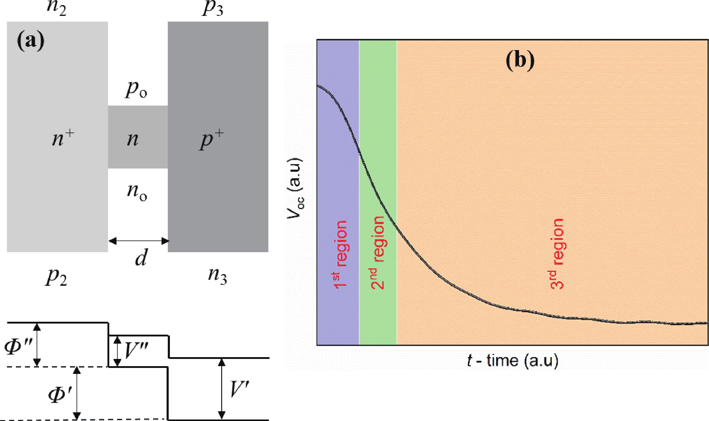
 DownLoad: