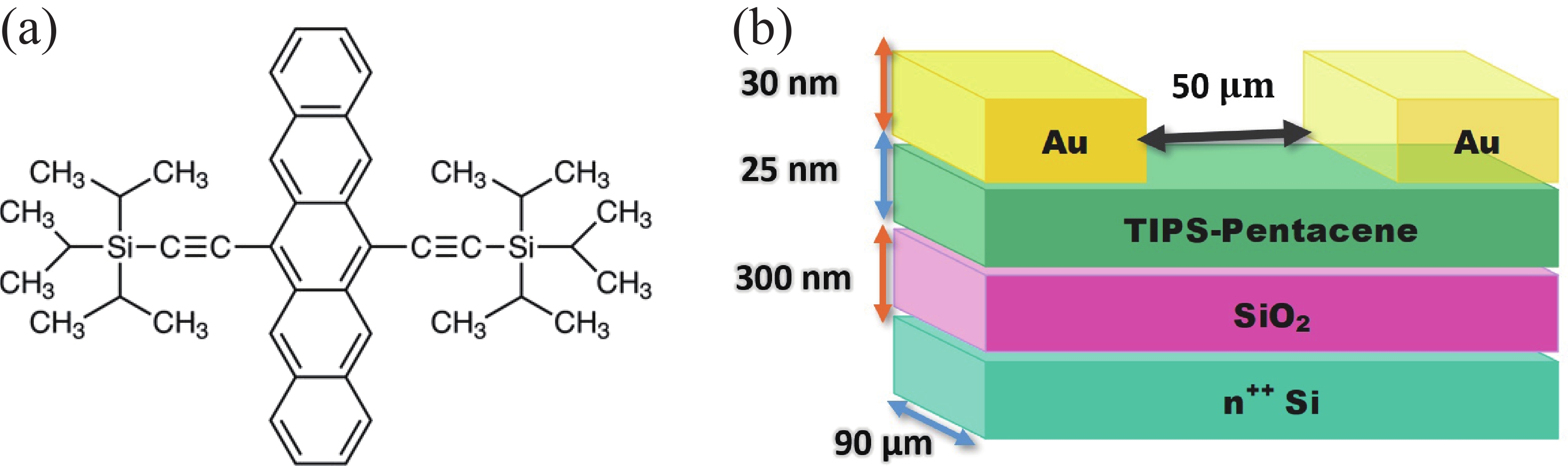
Fig. 1.
(Color online) (a) Chemical structure of Tips Pentacene, (b) structure and dimensions of device.
ARTICLES
Shubham Dadhich1, , Vivek Upadhyaya2 and Garima Mathur3
Corresponding author: Shubham Dadhich, saytoshubham@gmail.com
Abstract: As organic thin film transistors (OTFTs) are set to play a crucial role in flexible and cost-effective electronic applications, this paper investigates a high-mobility 6,13-bis(triisopropylsilylethynyl) Pentacene (TIPS-Pentacene) OTFT for use in flexible electronics. The development of such high-mobility devices necessitates precise device modeling to support technology optimisation and circuit design. The details of numerical simulation technique is discussed, in which, the electrical behavior of the device is well captured by fine tuning basic semiconductor equations. This technology computer-aided design (TCAD) has been validated with eprimental data. In addition, we have discussed about compact model fitting of the devices as well as parameter extraction procedure employed. This includes verification of ATLAS FEM based results against experimental data gained from fabricated OTFT devices. Simulations for p-type TFT-based inverter are also performed to assess the performance of compact model in simple circuit simulation.
Key words: TIPS-pentacene, organic semiconductor, compact modeling, TCAD modeling, OTFT, organic electronics
| [1] |
Lu M F, Huang M C, Lin J J. Emission distribution of volatile organic compounds of semiconductor and photovoltaic (TFT-LCD) industries. 2011 International Conference on Consumer Electronics, Communications and Networks (CECNet), 2011, 1206
|
| [2] |
Liu K, Ouyang B, Guo X J, et al. Advances in flexible organic field-effect transistors and their applications for flexible electronics. NPJ Flex Electron, 2022, 6, 1 doi: 10.1038/s41528-022-00133-3
|
| [3] |
Singh S, Takeda Y, Matsui H, et al. Flexible inkjet-printed dual-gate organic thin film transistors and PMOS inverters: Noise margin control by top gate. Org Electron, 2020, 85, 105847 doi: 10.1016/j.orgel.2020.105847
|
| [4] |
Chen C T, Yang H H. Inkjet printing of composite hole transport layers and bulk heterojunction structure for organic solar cells. Thin Solid Films, 2022, 751, 139217 doi: 10.1016/j.tsf.2022.139217
|
| [5] |
Zschieschang U, Klauk H. Organic transistors on paper: A brief review. J Mater Chem C, 2019, 7(19), 5522 doi: 10.1039/C9TC00793H
|
| [6] |
Tai Y H, Chou L S, Chiu H L, et al. Three-transistor AMOLED pixel circuit with threshold voltage compensation function using dual-gate IGZO TFT. IEEE Electron Device Lett, 2012, 33(3), 393 doi: 10.1109/LED.2011.2179282
|
| [7] |
Fu Y, Kong L A, Chen Y, et al. Flexible neuromorphic architectures based on self-supported multiterminal organic transistors. ACS Appl Mater Interfaces, 2018, 10(31), 26443 doi: 10.1021/acsami.8b07443
|
| [8] |
Khalil A, Ahmed Z, Touati F, et al. Review on organic solar cells. 2016 13th International Multi-Conference on Systems, Signals & Devices (SSD). Leipzig, Germany. IEEE, 2016, 342
|
| [9] |
Wang W, Ma D G, Gao Q. Optical programming/electrical erasing memory device based on low-voltage organic thin-film transistor. IEEE Trans Electron Devices, 2012, 59(5), 1510 doi: 10.1109/TED.2012.2187296
|
| [10] |
Sherwood CP, Elkington DC, Dickinson MR, et al. Organic Semiconductors for Optically Triggered Neural Interfacing: The Impact of Device Architecture in Determining Response Magnitude and Polarity. IEEE J Select Topics Quantum Electron, 2021, 27, 1
|
| [11] |
Chen G X, Peng G, Yu X P, et al. Multifunctional memory-synaptic hybrid optoelectronic transistors for neuromorphic computing. IEEE Trans Electron Devices, 2022, 69(7), 3997 doi: 10.1109/TED.2022.3173246
|
| [12] |
Wang S Y, Zhou S J, Tong Y H, et al. Dielectric selection for solution-processed high-mobility TIPS-pentacene microwire field-effect transistors. Adv Materials Inter, 2019, 6(13), 1801984 doi: 10.1002/admi.201801984
|
| [13] |
Kim J, Kim J, Ahn B, et al. Optimization and improvement of TIPS–pentacene transistors (OTFT) with UV–ozone and chemical treatments using an all-step solution process. Curr Appl Phys, 2015, 15(10), 1238 doi: 10.1016/j.cap.2015.07.012
|
| [14] |
Lee W, Park Y. Organic semiconductor/insulator polymer blends for high-performance organic transistors. Polymers, 2014, 6(4), 1057 doi: 10.3390/polym6041057
|
| [15] |
Chou L H, Na Y, Park C H, et al. Semiconducting small molecule/polymer blends for organic transistors. Polymer, 2020, 191, 122208 doi: 10.1016/j.polymer.2020.122208
|
| [16] |
Tang W, Li J H, Zhao J Q, et al. High-performance solution-processed low-voltage polymer thin-film transistors with low- $k$/high- $k$ bilayer gate dielectric. IEEE Electron Device Lett, 2015, 36(9), 950 doi: 10.1109/LED.2015.2462833
|
| [17] |
Boubaker A, Hafsi B, Lmimouni K, et al. A comparative TCAD simulations of a P-and N-type organic field effect transistors: Field-dependent mobility, bulk and interface traps models. J Mater Sci Mater Electron, 2017, 28(11), 7834 doi: 10.1007/s10854-017-6480-y
|
| [18] |
Montenegro Benavides C, Biele M, Schmidt O, et al. TIPS pentacene as a beneficial interlayer for organic photodetectors in imaging applications. IEEE Trans Electron Devices, 2018, 65(4), 1516 doi: 10.1109/TED.2018.2799705
|
| [19] |
Mustafa H A M, Jameel D A. Modeling and the main stages of spin coating process: A review. J Appl Sci Technol Trends, 2021, 2(2), 119 doi: 10.38094/jastt203109
|
| [20] |
Baccarani G, Gnani E, Gnudi A, et al. Theoretical foundations of the quantum drift-diffusion and density-gradient models. Solid State Electron, 2008, 52(4), 526 doi: 10.1016/j.sse.2007.10.051
|
| [21] |
Physics of Semiconductor Devices, Wiley Online Books, 2023
|
| [22] |
Khemissi S, Merabtine N, Azizi C, et al. An analytical model for the transconductance and drain conductance of GaAs MESFETs. 2010 XIth International Workshop on Symbolic and Numerical Methods, Modeling and Applications to Circuit Design (SM2ACD), 2010, 1
|
| [23] |
Estrada M, Cerdeira A, Mejia I, et al. Modeling the behavior of charge carrier mobility with temperature in thin-film polymeric transistors. Microelectron Eng, 2010, 87(12), 2565 doi: 10.1016/j.mee.2010.07.018
|
| [24] |
Cerdeira A, Estrada M, Soto-Cruz B S, et al. Modeling the behavior of amorphous oxide thin film transistors before and after bias stress. Microelectron Reliab, 2012, 52(11), 2532 doi: 10.1016/j.microrel.2012.04.017
|
| [25] |
Estrada M, Mejía I, Cerdeira A, et al. Mobility model for compact device modeling of OTFTs made with different materials. Solid State Electron, 2008, 52(5), 787 doi: 10.1016/j.sse.2007.11.007
|
| [26] |
Cerdeira A, Estrada M, Garcı́a R, et al. New procedure for the extraction of basic a-Si: H TFT model parameters in the linear and saturation regions. Solid State Electron, 2001, 45(7), 1077 doi: 10.1016/S0038-1101(01)00143-5
|
| [27] |
Iñiguez B, Picos R, Veksler D, et al. Universal compact model for long- and short-channel thin-film transistors. Solid State Electron, 2008, 52(3), 400 doi: 10.1016/j.sse.2007.10.027
|
| [28] |
Radha Krishnan R K, Dahal D, Paudel P R, et al. The influence of contact material and flat-band voltage on threshold voltage of organic field-effect transistors. Org Electron, 2022, 105, 106483 doi: 10.1016/j.orgel.2022.106483
|
| [29] |
Benson J, D’Halleweyn N V, Redman-White W, et al. A physically based relation between extracted threshold voltage and surface potential flat band voltage for MOSFET compact modeling. IEEE Trans Electron Devices, 2001, 48(5), 1019 doi: 10.1109/16.918258
|
| [30] |
Hankin A, Bedoya-Lora F E, Alexander J C, et al. Flat band potential determination: Avoiding the pitfalls. J Mater Chem A, 2019, 7(45), 26162 doi: 10.1039/C9TA09569A
|
| [31] |
Zhang P Y, Wan Q, Feng C H, et al. All regimes parasitic capacitances extraction using a multi-channel CBCM technique. IEEE Trans Semicond Manuf, 2017, 30(2), 121 doi: 10.1109/TSM.2017.2669317
|
| [32] |
Krishna R A, Suresh LP. A brief review on multi level inverter topologies. In: 2016 International Conference on Circuit, Power and Computing Technologies (ICCPCT), 2016, 1
|
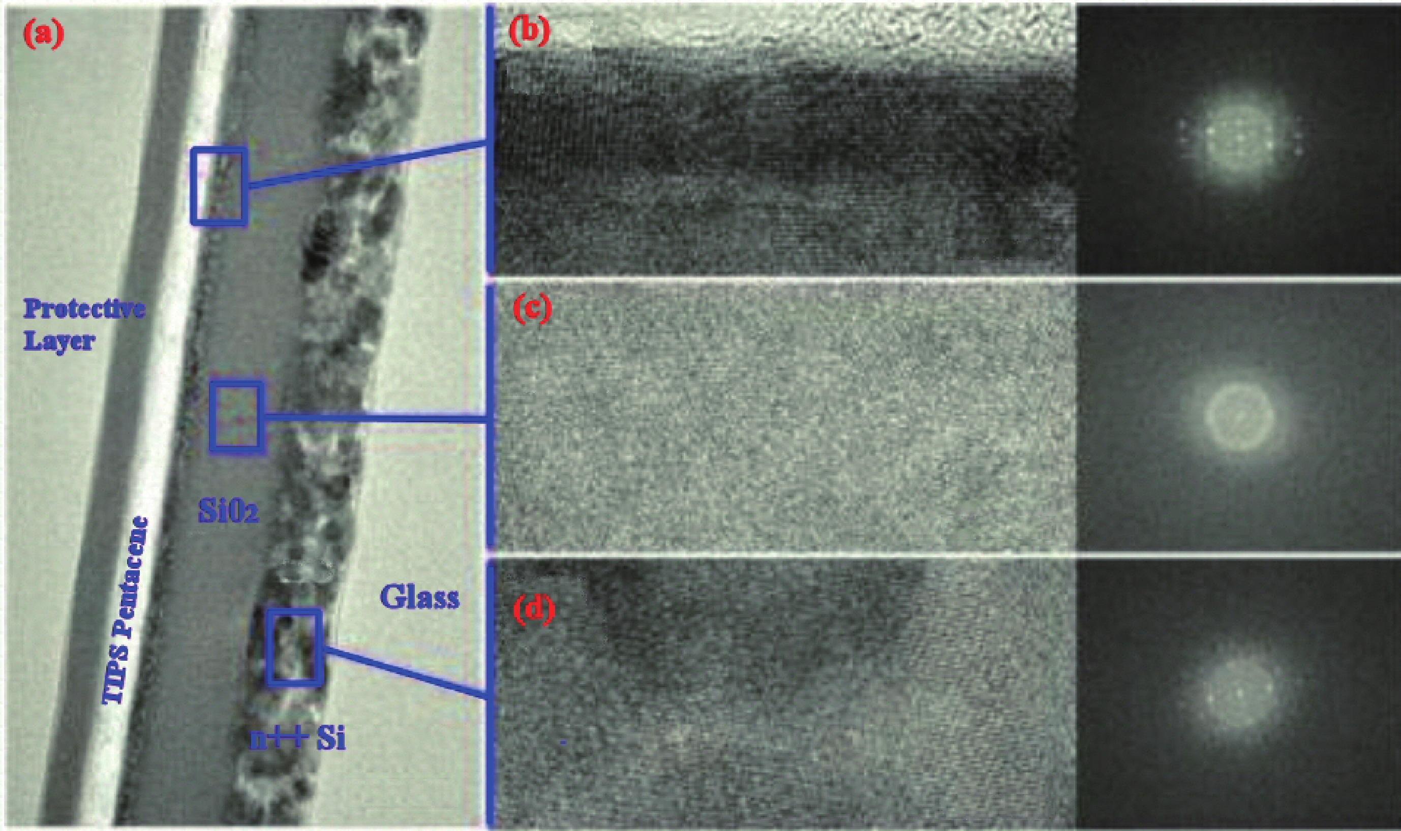
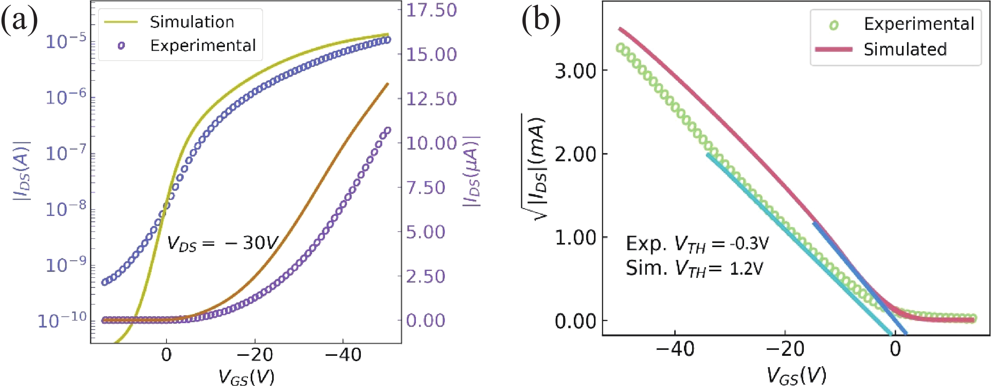
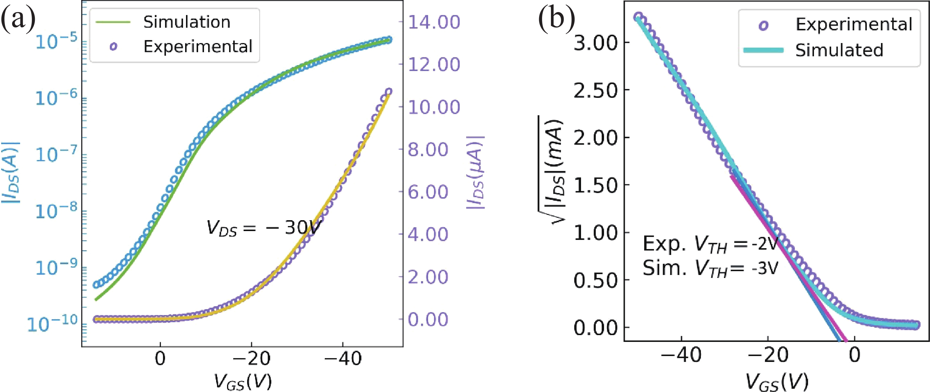
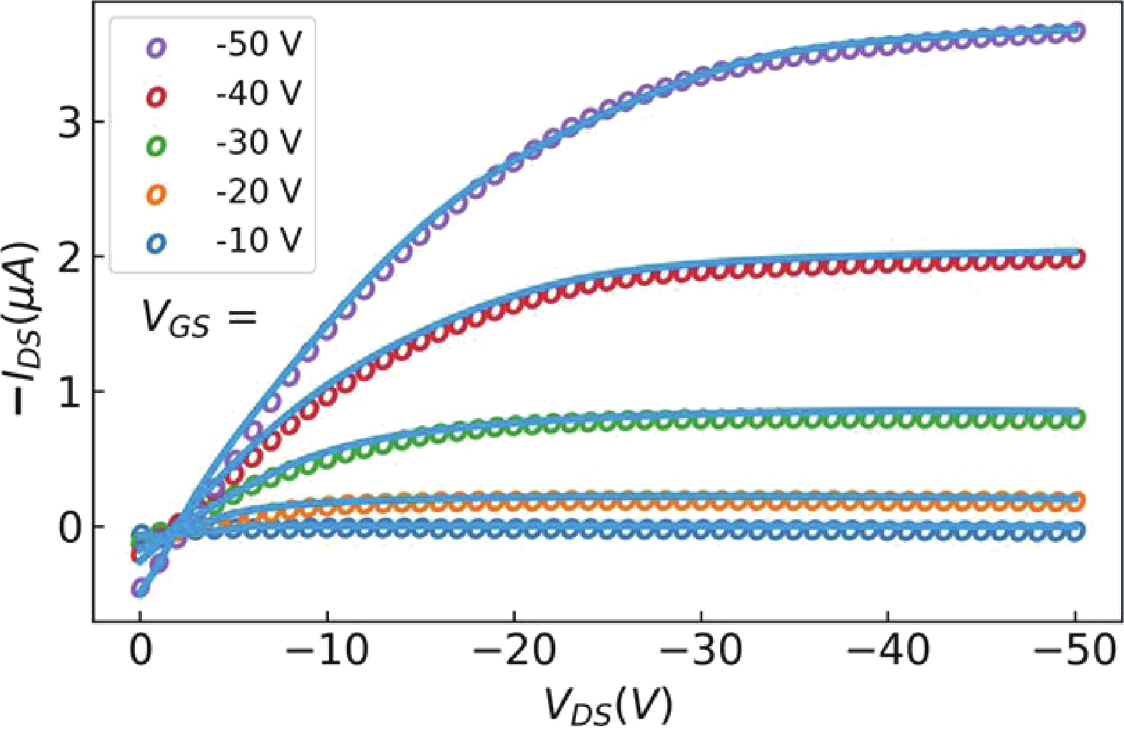
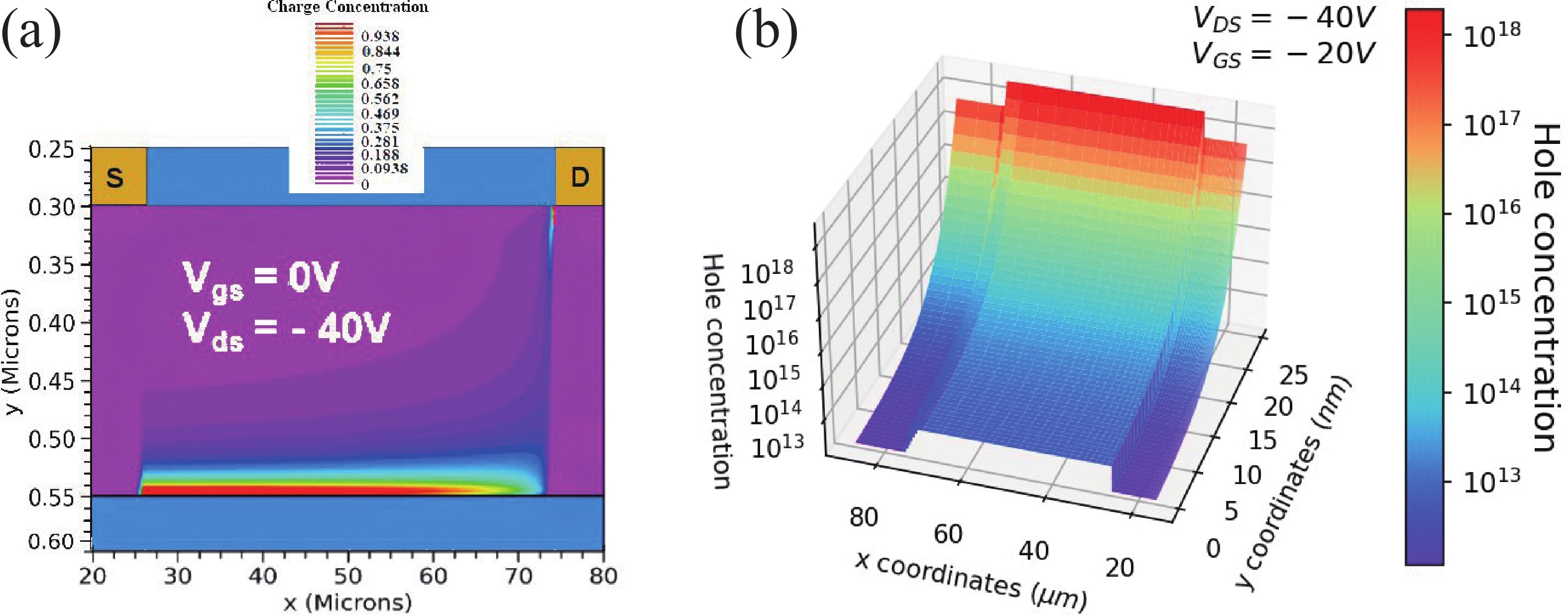
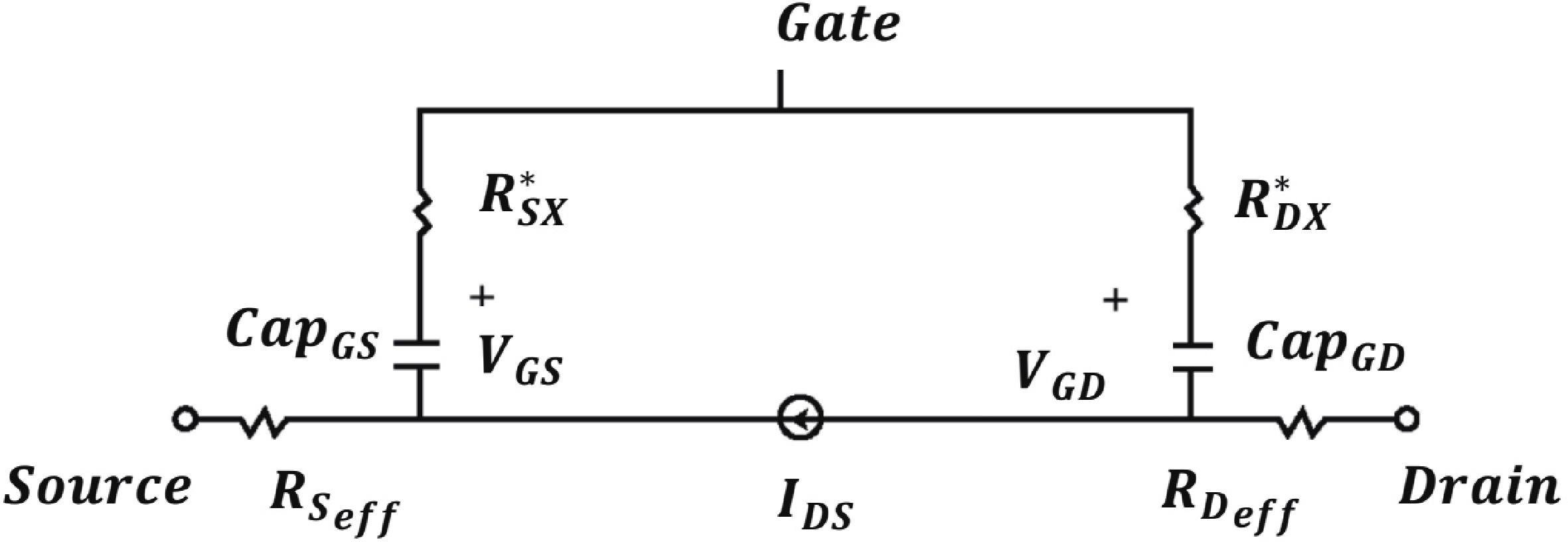
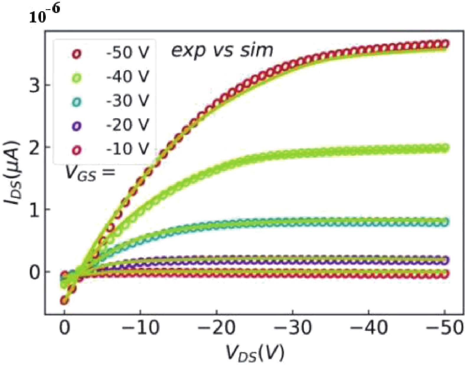
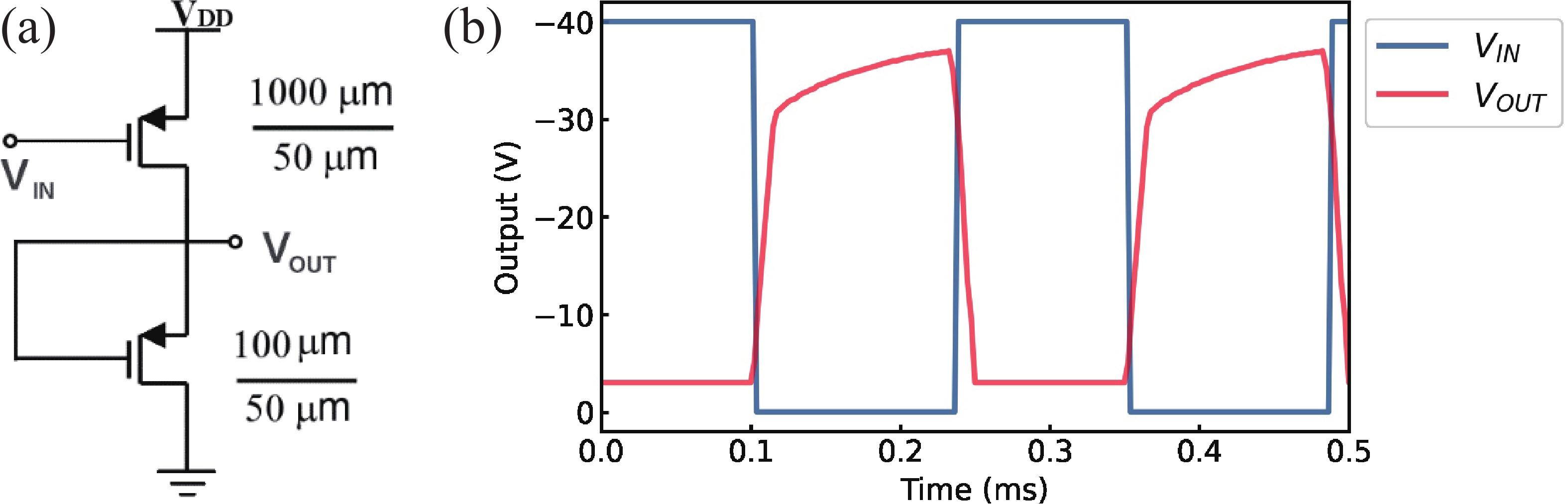
Table 1. Performance parameters comparison between simulated and experimented data of TIPS-Pentacene.
| Parameter | Experimented | Simulated | Unit |
| $ {\text{μ}}_{\mathrm{l}\mathrm{i}\mathrm{n}} $ ($ {\mathrm{V}}_{\mathrm{G}\mathrm{S}} $= 3 V) | 1.75 × 10⁻¹ | 1.96 × 10⁻² | cm2/(V·s) |
| $ {\mathrm{G}}_{\mathrm{m}} $ ($ {\mathrm{V}}_{\mathrm{G}\mathrm{S}}=3\mathrm{ }\mathrm{V}) $ | 4.20 × 10⁻⁷ | 4.42 × 10⁻⁷ | Siemens |
| $ {\text{μ}}_{\mathrm{s}\mathrm{a}\mathrm{t}} $($ {\mathrm{V}}_{\mathrm{G}\mathrm{S}}= $−30.0 V) | 8.37 × 10⁻¹ | 7.627 × 10⁻¹ | cm2/(V·s) |
| Sub-threshold slop (SS) | 5.40 | 6.83 | V/dec |
| $ {\mathrm{V}}_{\mathrm{T}\mathrm{H}} $ (Threshold) | −2.0 | −3.0 | Volt |
| $ {\mathrm{I}}_{\mathrm{o}\mathrm{n}}/{\mathrm{I}}_{\mathrm{o}\mathrm{f}\mathrm{f}} $ | 7.35 × 10⁶ | 7.56 × 10⁶ | (Ratio) |
 DownLoad: CSV
Table 2. Compact model fitting parameters of TIPS-Pentacene OTFT.
| Parameter | Description | Value | Unit |
| $ \lambda $ | Output conductance parameter | 3.0 × 10⁻⁶ | 1/V |
| $ M $ | Knee shape parameter | 1.32 | - |
| $ {\alpha }_{SAT} $ | Saturation modulation parameter | 0.69 | - |
| $ {V}_{MIN} $ | Minimum Value of $ {\mathrm{V}}_{\mathrm{g}\mathrm{t}\mathrm{e}} $ | −2.1 | V |
| $ \Delta $ | Transition width parameter | 2.8 | - |
| $ {V}_{TO} $ | Zero-bias threshold voltage | −0.89 | V |
| $ {\mu }_{0} $ | Conduction band mobility | 8.2 × 10⁻⁵ | m2/(V·s) |
| $ {T}_{OX} $ | Thin-oxide thickness | 3.0 × 10⁻⁷ | m |
| $ {V}_{AA} $ | Characteristic voltage for gate voltage | 1.0 | V |
| $ \Gamma $ | Power law mobility parameter | 1.05 | - |
| $ {V}_{0} $ | Characteristic voltage for deep states | 2.51×10⁻² | V |
| $ {G}_{MIN} $ | Minimum density of deep states | 1.0×10⁸ | m−3eV−1 |
| $ {N}_{C} $ | Effective conduction band DOS | 1.3 × 10¹⁵ | m−3 |
| $ {V}_{FB} $ | Flat band voltage (type-dependent) | −0.39 | V |
| $ {K}_{VT} $ | Threshold voltage temperature coefficient | -1.5 × 10⁻² | V/°C |
DownLoad: CSV
| [1] |
Lu M F, Huang M C, Lin J J. Emission distribution of volatile organic compounds of semiconductor and photovoltaic (TFT-LCD) industries. 2011 International Conference on Consumer Electronics, Communications and Networks (CECNet), 2011, 1206
|
| [2] |
Liu K, Ouyang B, Guo X J, et al. Advances in flexible organic field-effect transistors and their applications for flexible electronics. NPJ Flex Electron, 2022, 6, 1 doi: 10.1038/s41528-022-00133-3
|
| [3] |
Singh S, Takeda Y, Matsui H, et al. Flexible inkjet-printed dual-gate organic thin film transistors and PMOS inverters: Noise margin control by top gate. Org Electron, 2020, 85, 105847 doi: 10.1016/j.orgel.2020.105847
|
| [4] |
Chen C T, Yang H H. Inkjet printing of composite hole transport layers and bulk heterojunction structure for organic solar cells. Thin Solid Films, 2022, 751, 139217 doi: 10.1016/j.tsf.2022.139217
|
| [5] |
Zschieschang U, Klauk H. Organic transistors on paper: A brief review. J Mater Chem C, 2019, 7(19), 5522 doi: 10.1039/C9TC00793H
|
| [6] |
Tai Y H, Chou L S, Chiu H L, et al. Three-transistor AMOLED pixel circuit with threshold voltage compensation function using dual-gate IGZO TFT. IEEE Electron Device Lett, 2012, 33(3), 393 doi: 10.1109/LED.2011.2179282
|
| [7] |
Fu Y, Kong L A, Chen Y, et al. Flexible neuromorphic architectures based on self-supported multiterminal organic transistors. ACS Appl Mater Interfaces, 2018, 10(31), 26443 doi: 10.1021/acsami.8b07443
|
| [8] |
Khalil A, Ahmed Z, Touati F, et al. Review on organic solar cells. 2016 13th International Multi-Conference on Systems, Signals & Devices (SSD). Leipzig, Germany. IEEE, 2016, 342
|
| [9] |
Wang W, Ma D G, Gao Q. Optical programming/electrical erasing memory device based on low-voltage organic thin-film transistor. IEEE Trans Electron Devices, 2012, 59(5), 1510 doi: 10.1109/TED.2012.2187296
|
| [10] |
Sherwood CP, Elkington DC, Dickinson MR, et al. Organic Semiconductors for Optically Triggered Neural Interfacing: The Impact of Device Architecture in Determining Response Magnitude and Polarity. IEEE J Select Topics Quantum Electron, 2021, 27, 1
|
| [11] |
Chen G X, Peng G, Yu X P, et al. Multifunctional memory-synaptic hybrid optoelectronic transistors for neuromorphic computing. IEEE Trans Electron Devices, 2022, 69(7), 3997 doi: 10.1109/TED.2022.3173246
|
| [12] |
Wang S Y, Zhou S J, Tong Y H, et al. Dielectric selection for solution-processed high-mobility TIPS-pentacene microwire field-effect transistors. Adv Materials Inter, 2019, 6(13), 1801984 doi: 10.1002/admi.201801984
|
| [13] |
Kim J, Kim J, Ahn B, et al. Optimization and improvement of TIPS–pentacene transistors (OTFT) with UV–ozone and chemical treatments using an all-step solution process. Curr Appl Phys, 2015, 15(10), 1238 doi: 10.1016/j.cap.2015.07.012
|
| [14] |
Lee W, Park Y. Organic semiconductor/insulator polymer blends for high-performance organic transistors. Polymers, 2014, 6(4), 1057 doi: 10.3390/polym6041057
|
| [15] |
Chou L H, Na Y, Park C H, et al. Semiconducting small molecule/polymer blends for organic transistors. Polymer, 2020, 191, 122208 doi: 10.1016/j.polymer.2020.122208
|
| [16] |
Tang W, Li J H, Zhao J Q, et al. High-performance solution-processed low-voltage polymer thin-film transistors with low- $k$/high- $k$ bilayer gate dielectric. IEEE Electron Device Lett, 2015, 36(9), 950 doi: 10.1109/LED.2015.2462833
|
| [17] |
Boubaker A, Hafsi B, Lmimouni K, et al. A comparative TCAD simulations of a P-and N-type organic field effect transistors: Field-dependent mobility, bulk and interface traps models. J Mater Sci Mater Electron, 2017, 28(11), 7834 doi: 10.1007/s10854-017-6480-y
|
| [18] |
Montenegro Benavides C, Biele M, Schmidt O, et al. TIPS pentacene as a beneficial interlayer for organic photodetectors in imaging applications. IEEE Trans Electron Devices, 2018, 65(4), 1516 doi: 10.1109/TED.2018.2799705
|
| [19] |
Mustafa H A M, Jameel D A. Modeling and the main stages of spin coating process: A review. J Appl Sci Technol Trends, 2021, 2(2), 119 doi: 10.38094/jastt203109
|
| [20] |
Baccarani G, Gnani E, Gnudi A, et al. Theoretical foundations of the quantum drift-diffusion and density-gradient models. Solid State Electron, 2008, 52(4), 526 doi: 10.1016/j.sse.2007.10.051
|
| [21] |
Physics of Semiconductor Devices, Wiley Online Books, 2023
|
| [22] |
Khemissi S, Merabtine N, Azizi C, et al. An analytical model for the transconductance and drain conductance of GaAs MESFETs. 2010 XIth International Workshop on Symbolic and Numerical Methods, Modeling and Applications to Circuit Design (SM2ACD), 2010, 1
|
| [23] |
Estrada M, Cerdeira A, Mejia I, et al. Modeling the behavior of charge carrier mobility with temperature in thin-film polymeric transistors. Microelectron Eng, 2010, 87(12), 2565 doi: 10.1016/j.mee.2010.07.018
|
| [24] |
Cerdeira A, Estrada M, Soto-Cruz B S, et al. Modeling the behavior of amorphous oxide thin film transistors before and after bias stress. Microelectron Reliab, 2012, 52(11), 2532 doi: 10.1016/j.microrel.2012.04.017
|
| [25] |
Estrada M, Mejía I, Cerdeira A, et al. Mobility model for compact device modeling of OTFTs made with different materials. Solid State Electron, 2008, 52(5), 787 doi: 10.1016/j.sse.2007.11.007
|
| [26] |
Cerdeira A, Estrada M, Garcı́a R, et al. New procedure for the extraction of basic a-Si: H TFT model parameters in the linear and saturation regions. Solid State Electron, 2001, 45(7), 1077 doi: 10.1016/S0038-1101(01)00143-5
|
| [27] |
Iñiguez B, Picos R, Veksler D, et al. Universal compact model for long- and short-channel thin-film transistors. Solid State Electron, 2008, 52(3), 400 doi: 10.1016/j.sse.2007.10.027
|
| [28] |
Radha Krishnan R K, Dahal D, Paudel P R, et al. The influence of contact material and flat-band voltage on threshold voltage of organic field-effect transistors. Org Electron, 2022, 105, 106483 doi: 10.1016/j.orgel.2022.106483
|
| [29] |
Benson J, D’Halleweyn N V, Redman-White W, et al. A physically based relation between extracted threshold voltage and surface potential flat band voltage for MOSFET compact modeling. IEEE Trans Electron Devices, 2001, 48(5), 1019 doi: 10.1109/16.918258
|
| [30] |
Hankin A, Bedoya-Lora F E, Alexander J C, et al. Flat band potential determination: Avoiding the pitfalls. J Mater Chem A, 2019, 7(45), 26162 doi: 10.1039/C9TA09569A
|
| [31] |
Zhang P Y, Wan Q, Feng C H, et al. All regimes parasitic capacitances extraction using a multi-channel CBCM technique. IEEE Trans Semicond Manuf, 2017, 30(2), 121 doi: 10.1109/TSM.2017.2669317
|
| [32] |
Krishna R A, Suresh LP. A brief review on multi level inverter topologies. In: 2016 International Conference on Circuit, Power and Computing Technologies (ICCPCT), 2016, 1
|


Article views: 65 Times PDF downloads: 14 Times Cited by: 0 Times
Received: 15 September 2024 Revised: 18 April 2025 Online: Accepted Manuscript: 30 May 2025
| Citation: |
Shubham Dadhich, Vivek Upadhyaya, Garima Mathur. Fabrication, TCAD and compact model verification of TIPS-pentacene organic thin film transistor[J]. Journal of Semiconductors, 2025, In Press. doi: 10.1088/1674-4926/24090029
****
S Dadhich, V Upadhyaya, and G Mathur, Fabrication, TCAD and compact model verification of TIPS-pentacene organic thin film transistor[J]. J. Semicond., 2025, accepted doi: 10.1088/1674-4926/24090029

|
 Shubham Dadhich is an Assistant Professor at UPES, Dehradun, in Robotics Technology (R & D). With over 8+ years of research/teaching experience, he specializes in organic electronics, robotics and embedded systems. He has published many research papers and guided numerous student projects. A recipient of the Best Research Paper Award, he actively contributes to curriculum development, and national and international student industry skill development programs
 Vivek Upadhyaya is a Senior Member of IEEE with over 15 years of experience in academia and industry. He received his B.E. in ECE in 2009 and completed both his M.Tech and Ph.D. from MNIT Jaipur in 2016 and 2022, respectively, supported by the Visvesvaraya scholarship. His research interests include medical imaging, digital signal processing, compression techniques, AI, and machine learning. He has published extensively in journals and conferences and serves as a reviewer for reputed journals
 Garima Mathur is the Head and Professor of Electronics and Communication Engineering at Poornima College of Engineering (PCE), Jaipur, since January 2016. She holds a Ph.D. in Electrical and Electronics Engineering from MNIT Jaipur. With over two decades of academic experience, she specializes in wireless communication, MIMO-OFDM systems, and signal processing. Dr. Mathur has contributed extensively through research publications and conference participation
| [1] |
Lu M F, Huang M C, Lin J J. Emission distribution of volatile organic compounds of semiconductor and photovoltaic (TFT-LCD) industries. 2011 International Conference on Consumer Electronics, Communications and Networks (CECNet), 2011, 1206
|
| [2] |
Liu K, Ouyang B, Guo X J, et al. Advances in flexible organic field-effect transistors and their applications for flexible electronics. NPJ Flex Electron, 2022, 6, 1 doi: 10.1038/s41528-022-00133-3
|
| [3] |
Singh S, Takeda Y, Matsui H, et al. Flexible inkjet-printed dual-gate organic thin film transistors and PMOS inverters: Noise margin control by top gate. Org Electron, 2020, 85, 105847 doi: 10.1016/j.orgel.2020.105847
|
| [4] |
Chen C T, Yang H H. Inkjet printing of composite hole transport layers and bulk heterojunction structure for organic solar cells. Thin Solid Films, 2022, 751, 139217 doi: 10.1016/j.tsf.2022.139217
|
| [5] |
Zschieschang U, Klauk H. Organic transistors on paper: A brief review. J Mater Chem C, 2019, 7(19), 5522 doi: 10.1039/C9TC00793H
|
| [6] |
Tai Y H, Chou L S, Chiu H L, et al. Three-transistor AMOLED pixel circuit with threshold voltage compensation function using dual-gate IGZO TFT. IEEE Electron Device Lett, 2012, 33(3), 393 doi: 10.1109/LED.2011.2179282
|
| [7] |
Fu Y, Kong L A, Chen Y, et al. Flexible neuromorphic architectures based on self-supported multiterminal organic transistors. ACS Appl Mater Interfaces, 2018, 10(31), 26443 doi: 10.1021/acsami.8b07443
|
| [8] |
Khalil A, Ahmed Z, Touati F, et al. Review on organic solar cells. 2016 13th International Multi-Conference on Systems, Signals & Devices (SSD). Leipzig, Germany. IEEE, 2016, 342
|
| [9] |
Wang W, Ma D G, Gao Q. Optical programming/electrical erasing memory device based on low-voltage organic thin-film transistor. IEEE Trans Electron Devices, 2012, 59(5), 1510 doi: 10.1109/TED.2012.2187296
|
| [10] |
Sherwood CP, Elkington DC, Dickinson MR, et al. Organic Semiconductors for Optically Triggered Neural Interfacing: The Impact of Device Architecture in Determining Response Magnitude and Polarity. IEEE J Select Topics Quantum Electron, 2021, 27, 1
|
| [11] |
Chen G X, Peng G, Yu X P, et al. Multifunctional memory-synaptic hybrid optoelectronic transistors for neuromorphic computing. IEEE Trans Electron Devices, 2022, 69(7), 3997 doi: 10.1109/TED.2022.3173246
|
| [12] |
Wang S Y, Zhou S J, Tong Y H, et al. Dielectric selection for solution-processed high-mobility TIPS-pentacene microwire field-effect transistors. Adv Materials Inter, 2019, 6(13), 1801984 doi: 10.1002/admi.201801984
|
| [13] |
Kim J, Kim J, Ahn B, et al. Optimization and improvement of TIPS–pentacene transistors (OTFT) with UV–ozone and chemical treatments using an all-step solution process. Curr Appl Phys, 2015, 15(10), 1238 doi: 10.1016/j.cap.2015.07.012
|
| [14] |
Lee W, Park Y. Organic semiconductor/insulator polymer blends for high-performance organic transistors. Polymers, 2014, 6(4), 1057 doi: 10.3390/polym6041057
|
| [15] |
Chou L H, Na Y, Park C H, et al. Semiconducting small molecule/polymer blends for organic transistors. Polymer, 2020, 191, 122208 doi: 10.1016/j.polymer.2020.122208
|
| [16] |
Tang W, Li J H, Zhao J Q, et al. High-performance solution-processed low-voltage polymer thin-film transistors with low- $k$/high- $k$ bilayer gate dielectric. IEEE Electron Device Lett, 2015, 36(9), 950 doi: 10.1109/LED.2015.2462833
|
| [17] |
Boubaker A, Hafsi B, Lmimouni K, et al. A comparative TCAD simulations of a P-and N-type organic field effect transistors: Field-dependent mobility, bulk and interface traps models. J Mater Sci Mater Electron, 2017, 28(11), 7834 doi: 10.1007/s10854-017-6480-y
|
| [18] |
Montenegro Benavides C, Biele M, Schmidt O, et al. TIPS pentacene as a beneficial interlayer for organic photodetectors in imaging applications. IEEE Trans Electron Devices, 2018, 65(4), 1516 doi: 10.1109/TED.2018.2799705
|
| [19] |
Mustafa H A M, Jameel D A. Modeling and the main stages of spin coating process: A review. J Appl Sci Technol Trends, 2021, 2(2), 119 doi: 10.38094/jastt203109
|
| [20] |
Baccarani G, Gnani E, Gnudi A, et al. Theoretical foundations of the quantum drift-diffusion and density-gradient models. Solid State Electron, 2008, 52(4), 526 doi: 10.1016/j.sse.2007.10.051
|
| [21] |
Physics of Semiconductor Devices, Wiley Online Books, 2023
|
| [22] |
Khemissi S, Merabtine N, Azizi C, et al. An analytical model for the transconductance and drain conductance of GaAs MESFETs. 2010 XIth International Workshop on Symbolic and Numerical Methods, Modeling and Applications to Circuit Design (SM2ACD), 2010, 1
|
| [23] |
Estrada M, Cerdeira A, Mejia I, et al. Modeling the behavior of charge carrier mobility with temperature in thin-film polymeric transistors. Microelectron Eng, 2010, 87(12), 2565 doi: 10.1016/j.mee.2010.07.018
|
| [24] |
Cerdeira A, Estrada M, Soto-Cruz B S, et al. Modeling the behavior of amorphous oxide thin film transistors before and after bias stress. Microelectron Reliab, 2012, 52(11), 2532 doi: 10.1016/j.microrel.2012.04.017
|
| [25] |
Estrada M, Mejía I, Cerdeira A, et al. Mobility model for compact device modeling of OTFTs made with different materials. Solid State Electron, 2008, 52(5), 787 doi: 10.1016/j.sse.2007.11.007
|
| [26] |
Cerdeira A, Estrada M, Garcı́a R, et al. New procedure for the extraction of basic a-Si: H TFT model parameters in the linear and saturation regions. Solid State Electron, 2001, 45(7), 1077 doi: 10.1016/S0038-1101(01)00143-5
|
| [27] |
Iñiguez B, Picos R, Veksler D, et al. Universal compact model for long- and short-channel thin-film transistors. Solid State Electron, 2008, 52(3), 400 doi: 10.1016/j.sse.2007.10.027
|
| [28] |
Radha Krishnan R K, Dahal D, Paudel P R, et al. The influence of contact material and flat-band voltage on threshold voltage of organic field-effect transistors. Org Electron, 2022, 105, 106483 doi: 10.1016/j.orgel.2022.106483
|
| [29] |
Benson J, D’Halleweyn N V, Redman-White W, et al. A physically based relation between extracted threshold voltage and surface potential flat band voltage for MOSFET compact modeling. IEEE Trans Electron Devices, 2001, 48(5), 1019 doi: 10.1109/16.918258
|
| [30] |
Hankin A, Bedoya-Lora F E, Alexander J C, et al. Flat band potential determination: Avoiding the pitfalls. J Mater Chem A, 2019, 7(45), 26162 doi: 10.1039/C9TA09569A
|
| [31] |
Zhang P Y, Wan Q, Feng C H, et al. All regimes parasitic capacitances extraction using a multi-channel CBCM technique. IEEE Trans Semicond Manuf, 2017, 30(2), 121 doi: 10.1109/TSM.2017.2669317
|
| [32] |
Krishna R A, Suresh LP. A brief review on multi level inverter topologies. In: 2016 International Conference on Circuit, Power and Computing Technologies (ICCPCT), 2016, 1
|

 WeChat ID
Journal of Semiconductors © 2017 All Rights Reserved 京ICP备05085259号-2