J. Semicond. >  In Press

REVIEWS

Reconfigurable devices based on two-dimensional materials for logic and analog applications

Liutianyi Zhang1, 2, Ping-Heng Tan1, 2, and Jiangbin Wu1, 2,

+ Author Affiliations

 Corresponding author: Ping-Heng Tan, phtan@semi.ac.cn; Jiangbin Wu, jbwu@semi.ac.cn

DOI: 10.1088/1674-4926/24100005CSTR: 32376.14.1674-4926.24100005

PDF

Turn off MathJax

Abstract: In recent years, as the dimensions of the conventional semiconductor technology is approaching the physical limits, while the multifunction circuits are restricted by the relatively fixed characteristics of the traditional metal−oxide−semiconductor field-effect transistors, reconfigurable devices that can realize reconfigurable characteristics and multiple functions at device level have been seen as a promising method to improve integration density and reduce power consumption. Owing to the ultrathin structure, effective control of the electronic characteristics and ability to modulate structural defects, two-dimensional (2D) materials have been widely used to fabricate reconfigurable devices. In this review, we summarize the working principles and related logic applications of reconfigurable devices based on 2D materials, including generating tunable anti-ambipolar responses and demonstrating nonvolatile operations. Furthermore, we discuss the analog signal processing applications of anti-ambipolar transistors and the artificial intelligence hardware implementations based on reconfigurable transistors and memristors, respectively, therefore highlighting the outstanding advantages of reconfigurable devices in footprint, energy consumption and performance. Finally, we discuss the challenges of the 2D materials-based reconfigurable devices.

Key words: two-dimensional materialsreconfigurable devicesanti-ambipolar characteristicsnonvolatile devicesartificial intelligence hardware


[1]
Loubet N, Hook T, Montanini P, et al. Stacked nanosheet gate-all-around transistor to enable scaling beyond FinFET. 2017 Symposium on VLSI Technology, 2017, T230 doi: 10.23919/VLSIT.2017.7998183
[2]
Bravaix A, Hamparsoumian G, Sonzogni J, et al. CMOS scaling challenges for high performance and low power applications facing reliability criteria towards the decananometer range. J Phys: Conf Ser, 2023, 2548(1), 012003 doi: 10.1088/1742-6596/2548/1/012003
[3]
Radamson H H, He X B, Zhang Q Z, et al. Miniaturization of cmos. Micromachines, 2019, 10(5), 293 doi: 10.3390/mi10050293
[4]
Yin L, Cheng R Q, Wen Y, et al. Emerging 2D memory devices for in-memory computing. Adv Mater, 2021, 33(29), e2007081 doi: 10.1002/adma.202007081
[5]
Lee H E, Park J H, Kim T J, et al. Novel electronics for flexible and neuromorphic computing. Adv Funct Materials, 2018, 28(32), 1801690 doi: 10.1002/adfm.201801690
[6]
Heinzig A, Pregl S, Trommer J, et al. Reconfigurable NAND-NOR circuits fabricated by a CMOS printing technique. 2017 IEEE 12th Nanotechnology Materials and Devices Conference (NMDC), 2017, 179 doi: 10.1109/NMDC.2017.8350546
[7]
Peng R X, Wu Y H, Wang B L, et al. Programmable graded doping for reconfigurable molybdenum ditelluride devices. Nat Electron, 2023, 6, 852 doi: 10.1038/s41928-023-01056-1
[8]
Shingaya Y, Zulkefli A, Iwasaki T, et al. Dual-gate anti-ambipolar transistor with van der Waals ReS2/WSe2 heterojunction for reconfigurable logic operations. Adv Elect Materials, 2023, 9(1), 2200704 doi: 10.1002/aelm.202200704
[9]
Novoselov K S, Geim A K, Morozov S V, et al. Electric field effect in atomically thin carbon films. Science, 2004, 306(5696), 666 doi: 10.1126/science.1102896
[10]
Feng C Y, Wu W W, Liu H D, et al. Emerging opportunities for 2D materials in neuromorphic computing. Nanomaterials, 2023, 13(19), 2720 doi: 10.3390/nano13192720
[11]
Liu Y, Weiss N O, Duan X D, et al. Van der Waals heterostructures and devices. Nat Rev Mater, 2016, 1(9), 16042 doi: 10.1038/natrevmats.2016.42
[12]
Lemme M C, Akinwande D, Huyghebaert C, et al. 2D materials for future heterogeneous electronics. Nat Commun, 2022, 13(1), 1392 doi: 10.1038/s41467-022-29001-4
[13]
Liu C S, Chen H W, Wang S Y, et al. Two-dimensional materials for next-generation computing technologies. Nat Nanotechnol, 2020, 15(7), 545 doi: 10.1038/s41565-020-0724-3
[14]
Lukman S, Ding L, Xu L, et al. High oscillator strength interlayer excitons in two-dimensional heterostructures for mid-infrared photodetection. Nat Nanotechnol, 2020, 15(8), 675 doi: 10.1038/s41565-020-0717-2
[15]
Ye X L, Du Y N, Wang M Y, et al. Advances in the field of two-dimensional crystal-based photodetectors. Nanomaterials, 2023, 13(8), 1379 doi: 10.3390/nano13081379
[16]
Liu C Y, Guo J S, Yu L W, et al. Silicon/2D-material photodetectors: From near-infrared to mid-infrared. Light Sci Appl, 2021, 10(1), 123 doi: 10.1038/s41377-021-00551-4
[17]
Liu Z J, Gong X G, Cheng J R, et al. Wafer-scale synthesis of two-dimensional materials for integrated electronics. Chip, 2024, 3(1), 100080 doi: 10.1016/j.chip.2023.100080
[18]
Zhang L N, Dong J C, Ding F. Strategies, status, and challenges in wafer scale single crystalline two-dimensional materials synthesis. Chem Rev, 2021, 121(11), 6321 doi: 10.1021/acs.chemrev.0c01191
[19]
Chen T A, Chuu C P, Tseng C C, et al. Wafer-scale single-crystal hexagonal boron nitride monolayers on Cu (111). Nature, 2020, 579(7798), 219 doi: 10.1038/s41586-020-2009-2
[20]
Yang P F, Zhang S Q, Pan S Y, et al. Epitaxial growth of centimeter-scale single-crystal MoS2 monolayer on Au(111). ACS Nano, 2020, 14(4), 5036 doi: 10.1021/acsnano.0c01478
[21]
Fei W W, Trommer J, Lemme M C, et al. Emerging reconfigurable electronic devices based on two-dimensional materials: A review. InfoMat, 2022, 4(10), e12355 doi: 10.1002/inf2.12355
[22]
Mir S H, Yadav V K, Singh J K. Recent advances in the carrier mobility of two-dimensional materials: A theoretical perspective. ACS Omega, 2020, 5(24), 14203 doi: 10.1021/acsomega.0c01676
[23]
Gomes F O V, Pokle A, Marinkovic M, et al. High mobility solution processed MoS2 thin film transistors. Solid State Electron, 2019, 158, 75 doi: 10.1016/j.sse.2019.05.011
[24]
Cao W, Chu J H, Parto K, et al. A mode-balanced reconfigurable logic gate built in a van der Waals strata. NPJ 2D Mater Appl, 2021, 5, 20 doi: 10.1038/s41699-020-00198-6
[25]
Yan X D, Ma J H, Wu T, et al. Reconfigurable Stochastic neurons based on tin oxide/MoS2 hetero-memristors for simulated annealing and the Boltzmann machine. Nat Commun, 2021, 12, 5710 doi: 10.1038/s41467-021-26012-5
[26]
Chaves A, Azadani J G, Alsalman H, et al. Bandgap engineering of two-dimensional semiconductor materials. NPJ 2D Mater Appl, 2020, 4, 29 doi: 10.1038/s41699-020-00162-4
[27]
Jung D Y, Yang S Y, Park H, et al. Interface engineering for high performance graphene electronic devices. Nano Convergence, 2015, 2(1), 11 doi: 10.1186/s40580-015-0042-x
[28]
Sangwan V K, Beck M E, Henning A, et al. Self-aligned van der Waals heterojunction diodes and transistors. Nano Lett, 2018, 18(2), 1421 doi: 10.1021/acs.nanolett.7b05177
[29]
Xiong X, Kang J Y, Hu Q L, et al. Reconfigurable logic-in-memory and multilingual artificial synapses based on 2D heterostructures. Adv Funct Materials, 2020, 30(11), 1909645 doi: 10.1002/adfm.201909645
[30]
Liu H F, Wu J B, Ma J H, et al. A van der Waals interfacial junction transistor for reconfigurable fuzzy logic hardware. Nat Electron, 2024, 7, 876 doi: 10.1038/s41928-024-01256-3
[31]
Beck M E, Shylendra A, Sangwan V K, et al. Spiking neurons from tunable Gaussian heterojunction transistors. Nat Commun, 2020, 11(1), 1565 doi: 10.1038/s41467-020-15378-7
[32]
Meng Y, Wang W, Wang W, et al. Anti-ambipolar heterojunctions: Materials, devices, and circuits. Adv Mater, 2024, 36(17), e2306290 doi: 10.1002/adma.202306290
[33]
Chhowalla M, Jena D, Zhang H. Two-dimensional semiconductors for transistors. Nat Rev Mater, 2016, 1(11), 16052 doi: 10.1038/natrevmats.2016.52
[34]
Li H, Ling J Y, Lin J M, et al. Interface engineering in two-dimensional heterostructures towards novel emitters. J Semicond, 2023, 44(1), 011001 doi: 10.1088/1674-4926/44/1/011001
[35]
Wang H Y, Song X Y, Li Z X, et al. Recent advances in two-dimensional photovoltaic devices. J Semicond, 2024, 45(5), 051701 doi: 10.1088/1674-4926/45/5/051701
[36]
Thakar K, Lodha S. Multi-bit analog transmission enabled by electrostatically reconfigurable ambipolar and anti-ambipolar transport. ACS Nano, 2021, 15(12), 19692 doi: 10.1021/acsnano.1c07032
[37]
Jariwala D, Sangwan V K, Wu C C, et al. Gate-tunable carbon nanotube-MoS2 heterojunction p-n diode. Proc Natl Acad Sci USA, 2013, 110(45), 18076 doi: 10.1073/pnas.1317226110
[38]
Nourbakhsh A, Zubair A, Dresselhaus M S, et al. Transport properties of a MoS2/WSe2 heterojunction transistor and its potential for application. Nano Lett, 2016, 16(2), 1359 doi: 10.1021/acs.nanolett.5b04791
[39]
Roy T, Tosun M, Cao X, et al. Dual-gated MoS2/WSe2 van der Waals tunnel diodes and transistors. ACS Nano, 2015, 9(2), 2071 doi: 10.1021/nn507278b
[40]
Huo N J, Yang J H, Huang L, et al. Tunable polarity behavior and self-driven photoswitching in p-WSe2/n-WS2 heterojunctions. Small, 2015, 11(40), 5430 doi: 10.1002/smll.201501206
[41]
Huang M Q, Li S M, Zhang Z F, et al. Multifunctional high-performance van der Waals heterostructures. Nat Nanotechnol, 2017, 12(12), 1148 doi: 10.1038/nnano.2017.208
[42]
Li Y T, Wang Y, Huang L, et al. Anti-ambipolar field-effect transistors based on few-layer 2D transition metal dichalcogenides. ACS Appl Mater Interfaces, 2016, 8(24), 15574 doi: 10.1021/acsami.6b02513
[43]
Yan R S, Fathipour S, Han Y M, et al. Esaki diodes in van der Waals heterojunctions with broken-gap energy band alignment. Nano Lett, 2015, 15(9), 5791 doi: 10.1021/acs.nanolett.5b01792
[44]
Hayakawa R, Takahashi K, Zhong X H, et al. Reconfigurable logic-in-memory constructed using an organic antiambipolar transistor. Nano Lett, 2023, 23(17), 8339 doi: 10.1021/acs.nanolett.3c02726
[45]
Kobashi K, Hayakawa R, Chikyow T, et al. Multi-valued logic circuits based on organic anti-ambipolar transistors. Nano Lett, 2018, 18(7), 4355 doi: 10.1021/acs.nanolett.8b01357
[46]
Shim J, Oh S, Kang D H, et al. Phosphorene/rhenium disulfide heterojunction-based negative differential resistance device for multi-valued logic. Nat Commun, 2016, 7, 13413 doi: 10.1038/ncomms13413
[47]
Maeda K, Okabayashi N, Kano S, et al. Logic operations of chemically assembled single-electron transistor. ACS Nano, 2012, 6(3), 2798 doi: 10.1021/nn3003086
[48]
Wakayama Y, Hayakawa R. Antiambipolar transistor: A newcomer for future flexible electronics. Adv Funct Materials, 2020, 30(20), 1903724 doi: 10.1002/adfm.201903724
[49]
Yoo H, Kim C H. Multi-valued logic system: New opportunities from emerging materials and devices. J Mater Chem C, 2021, 9(12), 4092 doi: 10.1039/D1TC00148E
[50]
Kim C H, Hayakawa R, Wakayama Y. Fundamentals of organic anti-ambipolar ternary inverters. Adv Elect Materials, 2020, 6(3), 1901200 doi: 10.1002/aelm.201901200
[51]
Kim J B, Li J S, Choi Y, et al. Photosensitive graphene P-N junction transistors and ternary inverters. ACS Appl Mater Interfaces, 2018, 10(15), 12897 doi: 10.1021/acsami.8b00483
[52]
Wu E X, Xie Y, Liu Q Z, et al. Photoinduced doping to enable tunable and high-performance anti-ambipolar MoTe2/MoS2 heterotransistors. ACS Nano, 2019, 13(5), 5430 doi: 10.1021/acsnano.9b00201
[53]
Lim J H, Shim J, Kang B S, et al. Double negative differential transconductance characteristic: From device to circuit application toward quaternary inverter. Adv Funct Materials, 2019, 29(48), 1905540 doi: 10.1002/adfm.201905540
[54]
Jung K S, Heo K, Kim M J, et al. Double negative differential resistance device based on hafnium disulfide/pentacene hybrid structure. Adv Sci, 2020, 7(19), 2000991 doi: 10.1002/advs.202000991
[55]
Kim K H, Park H Y, Shim J, et al. A multiple negative differential resistance heterojunction device and its circuit application to ternary static random access memory. Nanoscale Horiz, 2020, 5(4), 654 doi: 10.1039/C9NH00631A
[56]
Yang B H, Chen J, Tu F B. Towards efficient generative AI and beyond-AI computing: New trends on ISSCC 2024 machine learning accelerators. J Semicond, 2024, 45(4), 040204 doi: 10.1088/1674-4926/45/4/040204
[57]
Zou X Q, Xu S, Chen X M, et al. Breaking the von Neumann bottleneck: Architecture-level processing-in-memory technology. Sci China Inf Sci, 2021, 64(6), 160404 doi: 10.1007/s11432-020-3227-1
[58]
Sasaki T, Ueno K, Taniguchi T, et al. Material and device structure designs for 2D memory devices based on the floating gate voltage trajectory. ACS Nano, 2021, 15(4), 6658 doi: 10.1021/acsnano.0c10005
[59]
Bertolazzi S, Bondavalli P, Roche S, et al. Nonvolatile memories based on graphene and related 2D materials. Adv Mater, 2019, 31(10), e1806663 doi: 10.1002/adma.201806663
[60]
Seo S, Lee J J, Lee H J, et al. Recent progress in artificial synapses based on two-dimensional van der Waals materials for brain-inspired computing. ACS Appl Electron Mater, 2020, 2(2), 371 doi: 10.1021/acsaelm.9b00694
[61]
Li D, Chen M Y, Sun Z Z, et al. Two-dimensional non-volatile programmable p-n junctions. Nat Nanotechnol, 2017, 12(9), 901 doi: 10.1038/nnano.2017.104
[62]
Yin L, Wang F, Cheng R Q, et al. Van der Waals heterostructure devices with dynamically controlled conduction polarity and multifunctionality. Adv Funct Materials, 2019, 29(1), 1804897 doi: 10.1002/adfm.201804897
[63]
Xiong X, Kang J Y, Liu S Y, et al. Nonvolatile logic and ternary content-addressable memory based on complementary black phosphorus and rhenium disulfide transistors. Adv Mater, 2022, 34(48), e2106321 doi: 10.1002/adma.202106321
[64]
Kumar A, Giubileo F, Sleziona S, et al. Temperature dependent black phosphorus transistor and memory. Nano Ex, 2023, 4(1), 014001 doi: 10.1088/2632-959X/acbe11
[65]
Liu L, Liu C S, Jiang L L, et al. Ultrafast non-volatile flash memory based on van der Waals heterostructures. Nat Nanotechnol, 2021, 16(8), 874 doi: 10.1038/s41565-021-00921-4
[66]
Hou X, Yan X, Liu C S, et al. Operation mode switchable charge-trap memory based on few-layer MoS2. Semicond Sci Technol, 2018, 33(3), 034001 doi: 10.1088/1361-6641/aaa79e
[67]
Zhang E Z, Wang W Y, Zhang C, et al. Tunable charge-trap memory based on few-layer MoS2. ACS Nano, 2015, 9(1), 612 doi: 10.1021/nn5059419
[68]
Zhang P F, Li D, Chen M Y, et al. Floating-gate controlled programmable non-volatile black phosphorus PNP junction memory. Nanoscale, 2018, 10(7), 3148 doi: 10.1039/C7NR08515J
[69]
Vu Q A, Shin Y S, Kim Y R, et al. Two-terminal floating-gate memory with van der Waals heterostructures for ultrahigh on/off ratio. Nat Commun, 2016, 7, 12725 doi: 10.1038/ncomms12725
[70]
Luo Z D, Zhang S Q, Liu Y, et al. Dual-ferroelectric-coupling-engineered two-dimensional transistors for multifunctional in-memory computing. ACS Nano, 2022, 16(2), 3362 doi: 10.1021/acsnano.2c00079
[71]
Sheng Z, Dong J G, Hu W N, et al. Reconfigurable logic-in-memory computing based on a polarity-controllable two-dimensional transistor. Nano Lett, 2023, 23(11), 5242 doi: 10.1021/acs.nanolett.3c01248
[72]
Sun X X, Zhu C G, Yi J L, et al. Reconfigurable logic-in-memory architectures based on a two-dimensional van der Waals heterostructure device. Nat Electron, 2022, 5, 752 doi: 10.1038/s41928-022-00858-z
[73]
Zhao Z J, Rakheja S, Zhu W J. Nonvolatile reconfigurable 2D Schottky barrier transistors. Nano Lett, 2021, 21(21), 9318 doi: 10.1021/acs.nanolett.1c03557
[74]
Seo S Y, Moon G, Okello O F N, et al. Reconfigurable photo-induced doping of two-dimensional van der Waals semiconductors using different photon energies. Nat Electron, 2021, 4, 38 doi: 10.1038/s41928-020-00512-6
[75]
Migliato Marega G, Zhao Y F, Avsar A, et al. Logic-in-memory based on an atomically thin semiconductor. Nature, 2020, 587(7832), 72 doi: 10.1038/s41586-020-2861-0
[76]
Hou X, Liu C S, Ding Y, et al. A logic-memory transistor with the integration of visible information sensing-memory-processing. Adv Sci, 2020, 7(21), 2002072 doi: 10.1002/advs.202002072
[77]
Cheng R Q, Wang F, Yin L, et al. High-performance, multifunctional devices based on asymmetric van der Waals heterostructures. Nat Electron, 2018, 1, 356 doi: 10.1038/s41928-018-0086-0
[78]
Yap W C, Jiang H, Liu J L, et al. Ferroelectric transistors with monolayer molybdenum disulfide and ultra-thin aluminum-doped hafnium oxide. Appl Phys Lett , 2017, 111(1), 013103 doi: 10.1063/1.4991877
[79]
Shekhawat A, Walters G, Yang N, et al. Data retention and low voltage operation of Al2O3/Hf0.5Zr0.5O2 based ferroelectric tunnel junctions. Nanotechnology, 2020, 31(39), 39LT01 doi: 10.1088/1361-6528/ab9cf7
[80]
Zhao R T, Zhao X Y, Liu H F, et al. Reconfigurable logic-memory hybrid device based on ferroelectric Hf0.5Zr0.5O2. IEEE Electron Device Lett, 2021, 42(8), 1164 doi: 10.1109/LED.2021.3089326
[81]
Lv L, Zhuge F W, Xie F J, et al. Reconfigurable two-dimensional optoelectronic devices enabled by local ferroelectric polarization. Nat Commun, 2019, 10(1), 3331 doi: 10.1038/s41467-019-11328-0
[82]
Zhu C C, Wang Y R, Wang F, et al. Nonvolatile reconfigurable broadband photodiodes based on BP/α-In2Se3 ferroelectric p–n junctions. Appl Phys Lett, 2022, 120(8), 083101 doi: 10.1063/5.0079535
[83]
Chen L, Wang T Y, Dai Y W, et al. Ultra-low power Hf0.5Zr0.5O2 based ferroelectric tunnel junction synapses for hardware neural network applications. Nanoscale, 2018, 10(33), 15826 doi: 10.1039/C8NR04734K
[84]
Wang Y R, Wang F, Wang Z X, et al. Reconfigurable photovoltaic effect for optoelectronic artificial synapse based on ferroelectric p-n junction. Nano Res, 2021, 14(11), 4328 doi: 10.1007/s12274-021-3833-x
[85]
Tsai M Y, Huang C T, Lin C Y, et al. A reconfigurable transistor and memory based on a two-dimensional heterostructure and photoinduced trapping. Nat Electron, 2023, 6, 755 doi: 10.1038/s41928-023-01034-7
[86]
Bae J H, Kim H, Kwon D, et al. Reconfigurable field-effect transistor as a synaptic device for XNOR binary neural network. IEEE Electron Device Lett, 2019, 40(4), 624 doi: 10.1109/LED.2019.2898448
[87]
Yin L, Cheng R Q, Wang Z X, et al. Two-dimensional unipolar memristors with logic and memory functions. Nano Lett, 2020, 20(6), 4144 doi: 10.1021/acs.nanolett.0c00002
[88]
Liu C S, Chen H W, Hou X, et al. Small footprint transistor architecture for photoswitching logic and in situ memory. Nat Nanotechnol, 2019, 14(7), 662 doi: 10.1038/s41565-019-0462-6
[89]
Liu C S, Yan X, Song X F, et al. A semi-floating gate memory based on van der Waals heterostructures for quasi-non-volatile applications. Nat Nanotechnol, 2018, 13(5), 404 doi: 10.1038/s41565-018-0102-6
[90]
Li J Y, Zhang H, Ding Y, et al. A non-volatile AND gate based on Al2O3/HfO2/Al2O3 charge-trap stack for in situ storage applications. Sci Bull, 2019, 64(20), 1518 doi: 10.1016/j.scib.2019.08.012
[91]
Zhang X H, Peng B. The twisted two-dimensional ferroelectrics. J Semicond, 2023, 44(1), 011002 doi: 10.1088/1674-4926/44/1/011002
[92]
Yao H, Wu E X, Liu J. Frequency doubler based on a single MoTe2/MoS2 anti-ambipolar heterostructure. Appl Phys Lett, 2020, 117(12), 1231, 03 doi: 10.1063/5.0018882
[93]
Lee M, Kim T W, Park C Y, et al. Graphene bridge heterostructure devices for negative differential transconductance circuit applications. Nanomicro Lett, 2022, 15(1), 22 doi: 10.1007/s40820-022-01001-5
[94]
Yuce M R, Liu W T. A low-power multirate differential PSK receiver for space applications. IEEE Trans Veh Technol, 2005, 54(6), 2074 doi: 10.1109/TVT.2005.858196
[95]
Das S, Das S. Digital keying enabled by reconfigurable 2D modulators. Adv Mater, 2022, 34(43), e2203753 doi: 10.1002/adma.202203753
[96]
Jariwala D, Sangwan V K, Seo J T, et al. Large-area, low-voltage, antiambipolar heterojunctions from solution-processed semiconductors. Nano Lett, 2015, 15(1), 416 doi: 10.1021/nl5037484
[97]
Crespo J L, Duro R J, Pena F L. Gaussian synapse ANNs in multi- and hyperspectral image data analysis. IEEE Trans Instrum Meas, 2003, 52(3), 724 doi: 10.1109/TIM.2003.814693
[98]
Sebastian A, Pannone A, Subbulakshmi Radhakrishnan S, et al. Gaussian synapses for probabilistic neural networks. Nat Commun, 2019, 10(1), 4199 doi: 10.1038/s41467-019-12035-6
[99]
Yan X D, Qian J H, Ma J H, et al. Reconfigurable mixed-kernel heterojunction transistors for personalized support vector machine classification. Nat Electron, 2023, 6, 862 doi: 10.1038/s41928-023-01042-7
[100]
Sangwan V K, Hersam M C. Neuromorphic nanoelectronic materials. Nat Nanotechnol, 2020, 15(7), 517 doi: 10.1038/s41565-020-0647-z
[101]
Maass W. Networks of spiking neurons: The third generation of neural network models. Neural Netw, 1997, 10(9), 1659 doi: 10.1016/S0893-6080(97)00011-7
[102]
Gao L G, Chen P Y, Yu S M. NbOx based oscillation neuron for neuromorphic computing. Appl Phys Lett, 2017, 111(10), 103503 doi: 10.1063/1.4991917
[103]
Wang J Y, Teng C J, Zhang Z Y, et al. A scalable artificial neuron based on ultrathin two-dimensional titanium oxide. ACS Nano, 2021, 15(9), 15123 doi: 10.1021/acsnano.1c05565
[104]
Wang Z R, Joshi S, Savel’ev S, et al. Fully memristive neural networks for pattern classification with unsupervised learning. Nat Electron, 2018, 1, 137 doi: 10.1038/s41928-018-0023-2
[105]
Wang Z, Crafton B, Gomez J, et al. Experimental demonstration of ferroelectric spiking neurons for unsupervised clustering. 2018 IEEE International Electron Devices Meeting (IEDM), 2018, 13.3.1 doi: 10.1109/IEDM.2018.8614586
[106]
Sangwan V K, Jariwala D, Kim I S, et al. Gate-tunable memristive phenomena mediated by grain boundaries in single-layer MoS2. Nat Nanotechnol, 2015, 10(5), 403 doi: 10.1038/nnano.2015.56
[107]
Wang M, Cai S H, Pan C, et al. Robust memristors based on layered two-dimensional materials. Nat Electron, 2018, 1, 130 doi: 10.1038/s41928-018-0021-4
[108]
Shi Y Y, Liang X H, Yuan B, et al. Electronic synapses made of layered two-dimensional materials. Nat Electron, 2018, 1, 458 doi: 10.1038/s41928-018-0118-9
[109]
Sun L F, Hwang G, Choi W, et al. Ultralow switching voltage slope based on two-dimensional materials for integrated memory and neuromorphic applications. Nano Energy, 2020, 69, 104472 doi: 10.1016/j.nanoen.2020.104472
[110]
Zhu X J, Li D, Liang X G, et al. Ionic modulation and ionic coupling effects in MoS2 devices for neuromorphic computing. Nat Mater, 2019, 18(2), 141 doi: 10.1038/s41563-018-0248-5
[111]
Zhang F, Zhang H R, Krylyuk S, et al. Electric-field induced structural transition in vertical MoTe2- and Mo1- xW xTe2-based resistive memories. Nat Mater, 2019, 18(1), 55 doi: 10.1038/s41563-018-0234-y
[112]
Feng X W, Li Y D, Wang L, et al. A fully printed flexible MoS2 memristive artificial synapse with femtojoule switching energy. Adv Elect Mater, 2019, 5(12), 1900740 doi: 10.1002/aelm.201900740
[113]
Wang K Y, Li L T, Zhao R J, et al. A pure 2H-MoS2 nanosheet-based memristor with low power consumption and linear multilevel storage for artificial synapse emulator. Adv Elect Mater, 2020, 6(3), 1901342 doi: 10.1002/aelm.201901342
[114]
Cai F X, Kumar S, Van Vaerenbergh T, et al. Power-efficient combinatorial optimization using intrinsic noise in memristor Hopfield neural networks. Nat Electron, 2020, 3, 409 doi: 10.1038/s41928-020-0436-6
[115]
Jiang H, Belkin D, Savel’ev S E, et al. A novel true random number generator based on a stochastic diffusive memristor. Nat Commun, 2017, 8(1), 882 doi: 10.1038/s41467-017-00869-x
[116]
Kalita H, Krishnaprasad A, Choudhary N, et al. Artificial neuron using vertical MoS2/graphene threshold switching memristors. Sci Rep, 2019, 9(1), 53 doi: 10.1038/s41598-018-35828-z
[117]
Bez R, Camerlenghi E, Modelli A, et al. Introduction to flash memory. Proc IEEE, 2003, 91(4), 489 doi: 10.1109/JPROC.2003.811702
[118]
Wang D, Zhang Z C, Li B, et al. Synthesis of two-dimensional/one-dimensional heterostructures with tunable width. J Semicond, 2021, 42(9), 092001 doi: 10.1088/1674-4926/42/9/092001
[119]
Zhao T G, Guo J X, Li T T, et al. Substrate engineering for wafer-scale two-dimensional material growth: Strategies, mechanisms, and perspectives. Chem Soc Rev, 2023, 52(5), 1650 doi: 10.1039/D2CS00657J
[120]
Quellmalz A, Wang X J, Sawallich S, et al. Large-area integration of two-dimensional materials and their heterostructures by wafer bonding. Nat Commun, 2021, 12(1), 917 doi: 10.1038/s41467-021-21136-0
[121]
Chen S C, Mahmoodi M R, Shi Y Y, et al. Wafer-scale integration of two-dimensional materials in high-density memristive crossbar arrays for artificial neural networks. Nat Electron, 2020, 3, 638 doi: 10.1038/s41928-020-00473-w
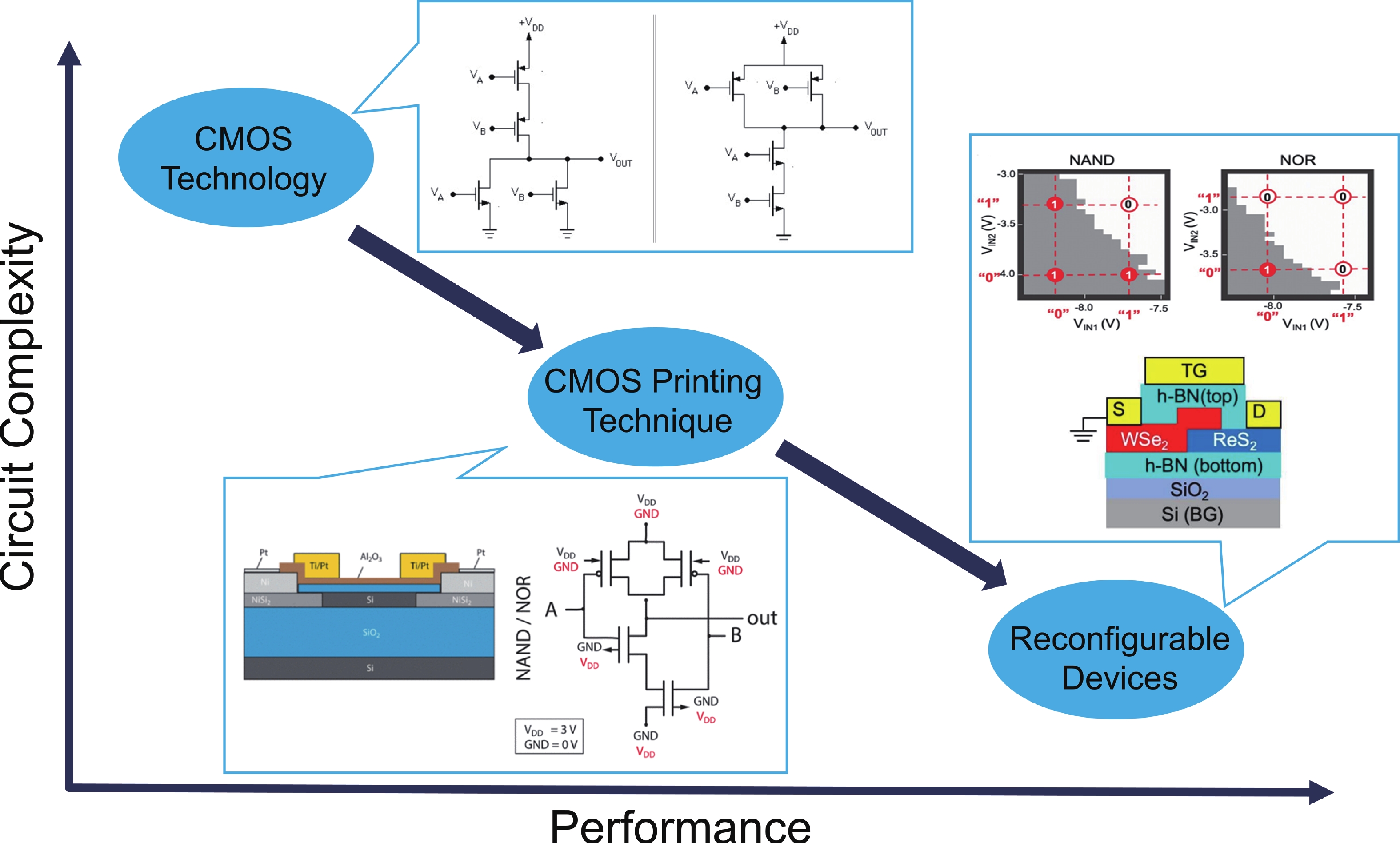
Fig. 1.  (Color online) The comparison of the circuit complexity and performance of diverse technologies in implementing the NAND/NOR logic gates circuit. Conventional CMOS technologies are unable to realize both NAND and NOR operations within a single circuit due to the fixed polarity of MOSFETs. Compared to the fixed polarity of CMOS transistors, a CMOS printing technique[6] was used to integrate intrinsic silicon nanowires to construct transistors capable of being programmed as either n-type or p-type. Consequently, utilizing only four transistors allows for the fabrication of a reconfigurable NAND/NOR circuit. Moreover, the output anti-ambipolar characteristics of a reconfigurable dual-gated transistor[8] based on 2D n-ReS2/p-WSe2 heterojunction are able to be controlled by the input voltages, therefore a single transistor can accomplish all the two-input logic operations including NAND and NOR, thereby significantly reducing the circuit complexity and enhancing the functionality of circuits.

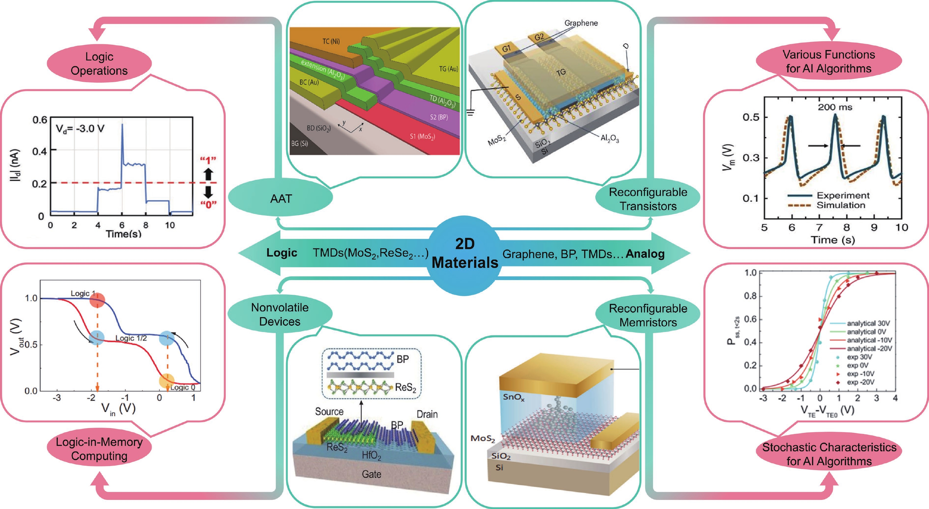
Fig. 2.  (Color online) An overview of the recent reconfigurable devices based on 2D materials for logic and analog applications[8, 25, 2831].

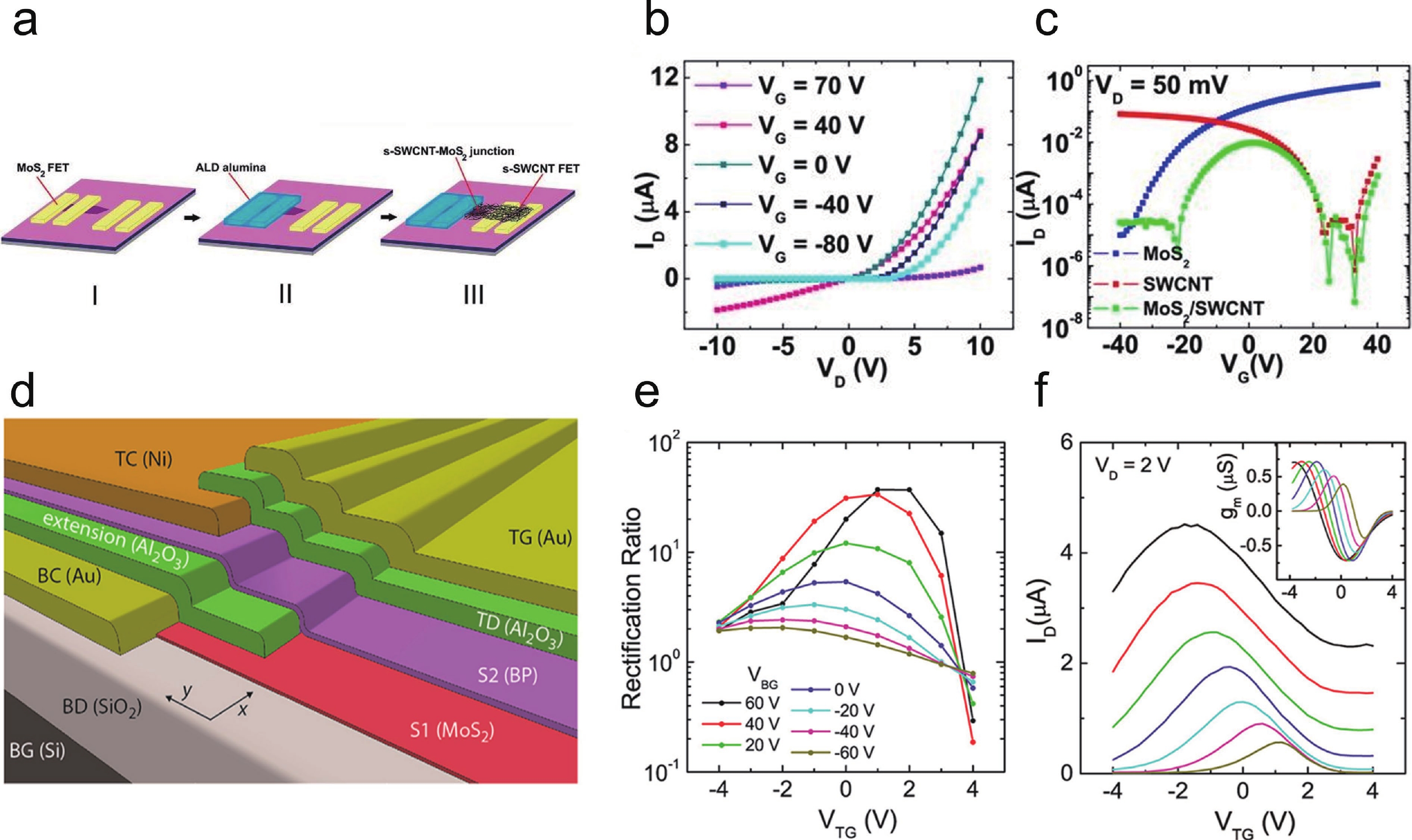
Fig. 3.  (Color online) Typical AAT devices. (a) Schematic of the fabrication process, (b) output characteristics and (c) transfer characteristics of the gate-tunable SWCNT/MoS2 heterojunction diode[37]. (d) Schematic illustration of the self-aligned heterojunction transistor. (e) The rectification ratios of the BP/MoS2 at different bottom-gate bias (VBG) values. (f) IDVTG characteristics of the heterojunction transistor at different VBG. The inset in (f) shows the variation in transconductance[28].

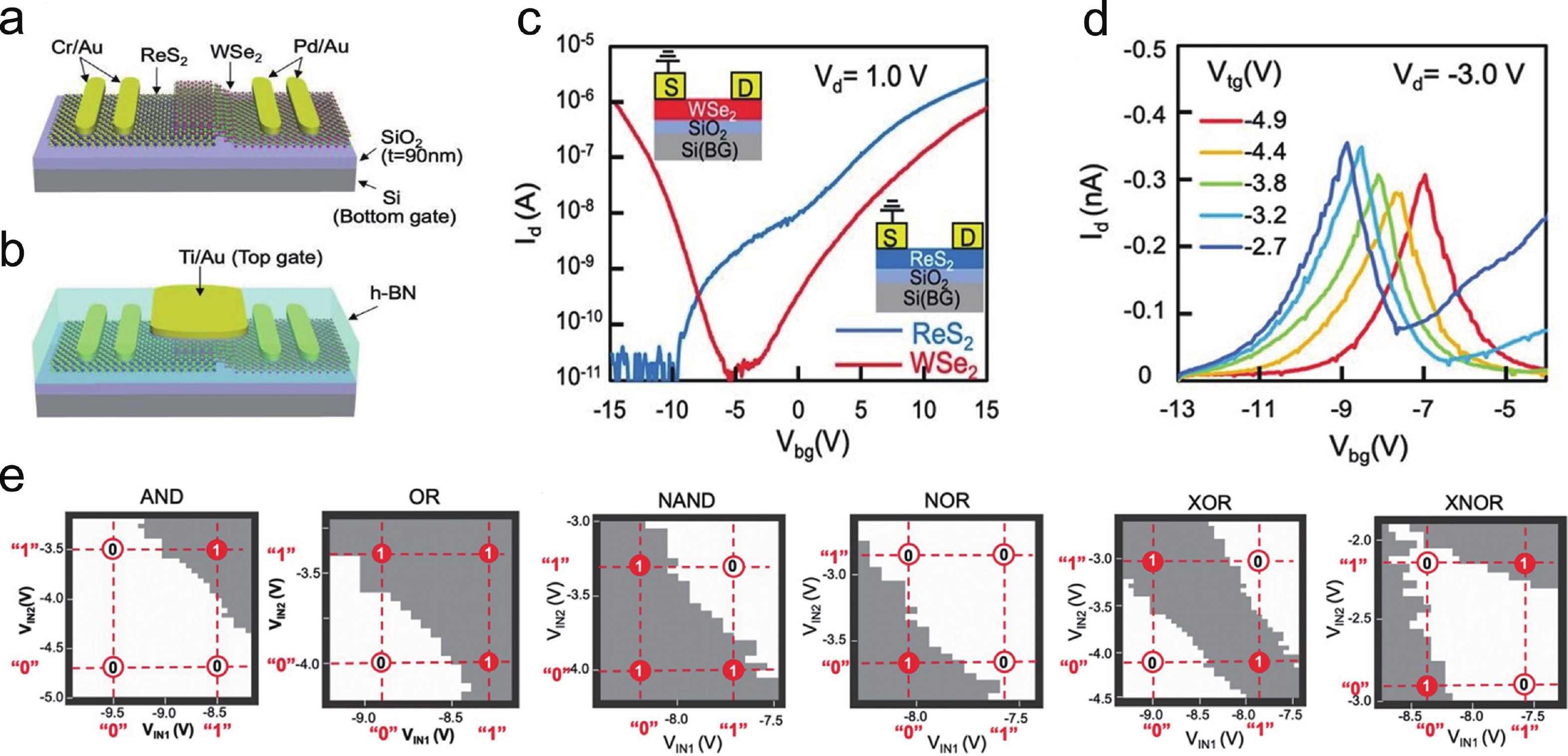
Fig. 4.  (Color online) 2D reconfigurable AAT devices applied to reconfigurable logic circuits. Schematic illustrations of (a) the bottom-gate ReS2/WSe2 AAT and (b) the dual-gate ReS2/WSe2 AAT. (c) The transfer curves of the ReS2-FET (blue) and WSe2-FET (red) with Vd at 1.0 V. (d) The transfer characteristics of the dual-gate ReS2/WSe2 AAT. (e) The two-input logic operations are able to be demonstrated in a single dual-gate ReS2/WSe2 AAT[8].

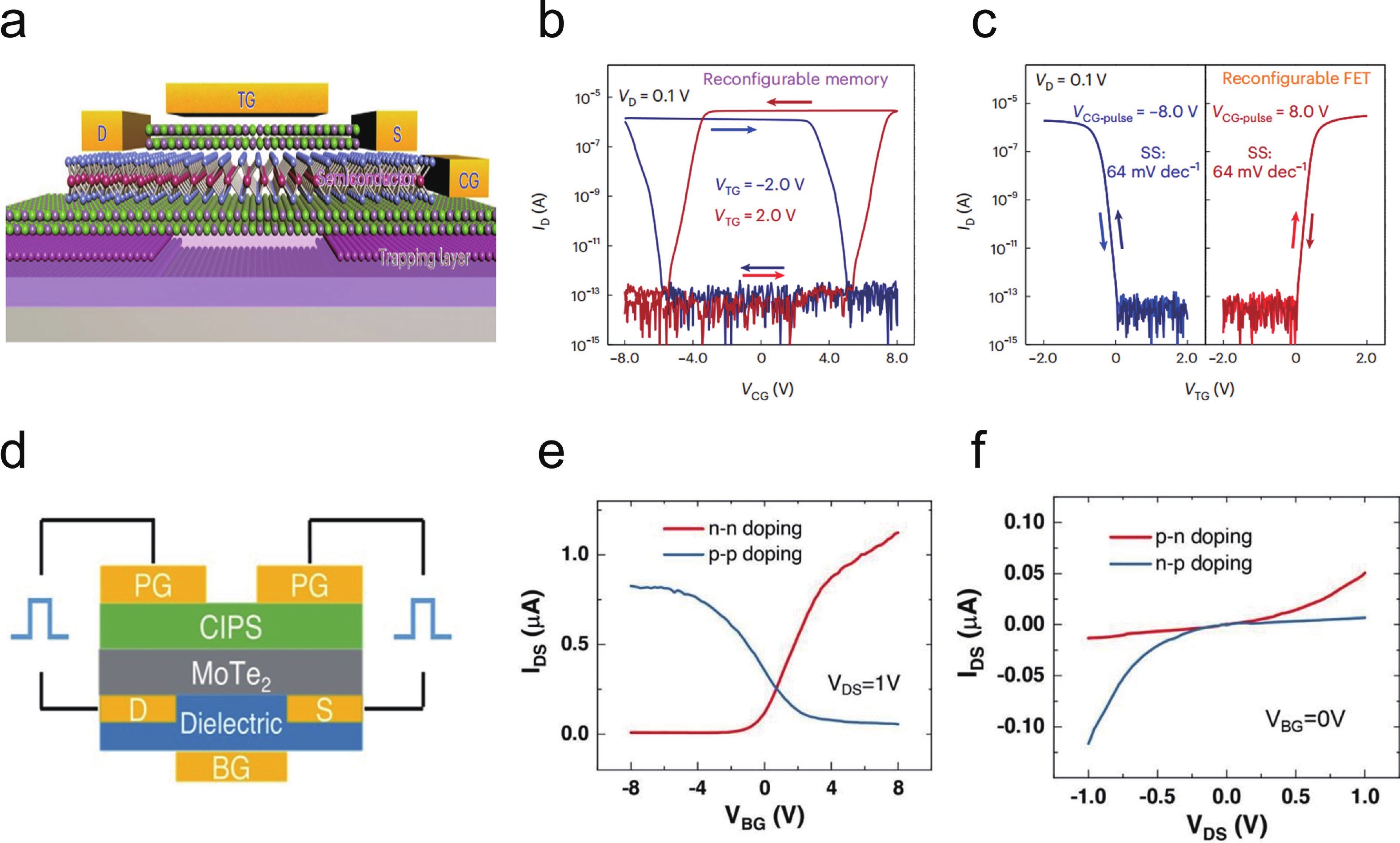
Fig. 5.  (Color online) Nonvolatile reconfigurable multifunctional devices. (a) The schematic of the partial-floating-gate FET. The transfer characteristics of the partial-floating-gate FET acquired in (b) the reconfigurable memory mode and (c) the reconfigurable FET mode[72]. (d) The schematic of the reconfigurable transistor based on ferroelectric CuInP2S6/MoTe2 heterostructure. (e) Transfer curves of the CuInP2S6/MoTe2 heterostructure transistor in symmetrically programming state (p−p and n−n doping). (f) Output curves of the transistor in asymmetrically programming state (p−n and n−p doping)[73].

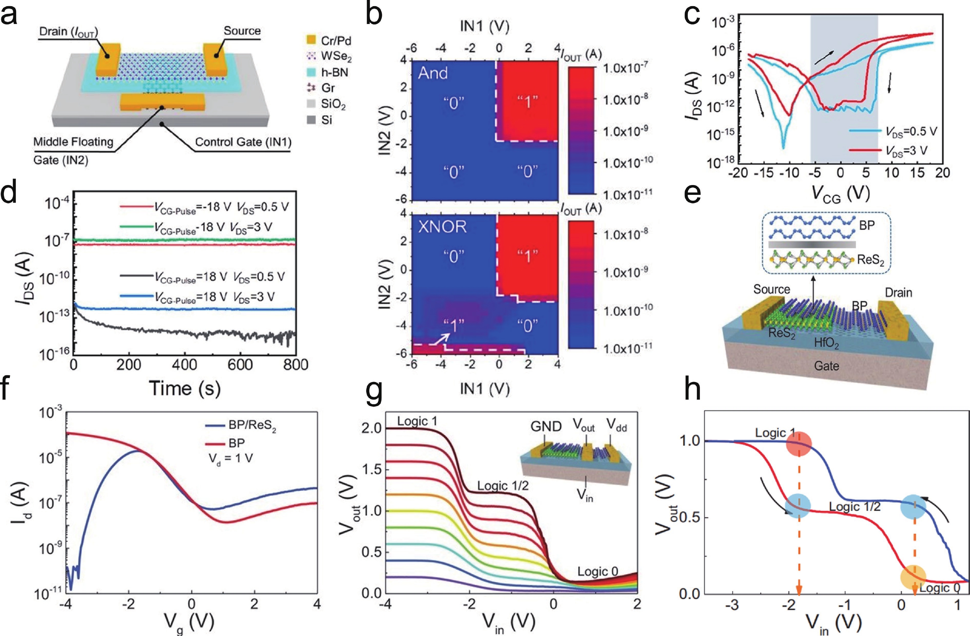
Fig. 6.  (Color online) Nonvolatile devices used for logic-in-memory computing. (a) The schematic of the middle-floating-gate FET (MFGFET) based on WSe2/h-BN/graphene vdWH. (b) Reconfigurable logic operations achieved in a single MFGFET. (c) The transfer curves of the MFGFET show a memory window. (d) The retention characteristics of the MFGFET[71]. (e) Schematic illustration of the BP/ReS2 heterostructure device. (f) The transfer curves of the BP-FET (blue) and the BP/ReS2-FET (red), respectively. (g) The output characteristics of the ternary logic circuit based on a BP/ReS2 heterojunction device. (h) The double swept voltage transfer characteristics of the ternary logic inverter circuit[29].

Fig. 7.  (Color online) 2D reconfigurable AAT devices applied to analog signal processing. (a) The three-dimensional schematic of the dual-gate WSe2 transistor. (b) The transfer curves and the respective biasing configurations of the four modes (n-FET, p-FET, ambipolar, and anti-ambipolar) of the WSe2 transistor. The frequency and phase operations achieved by the WSe2 transistor in the condition of dark environment and (c) ambipolar or (d) anti-ambipolar modes[36].

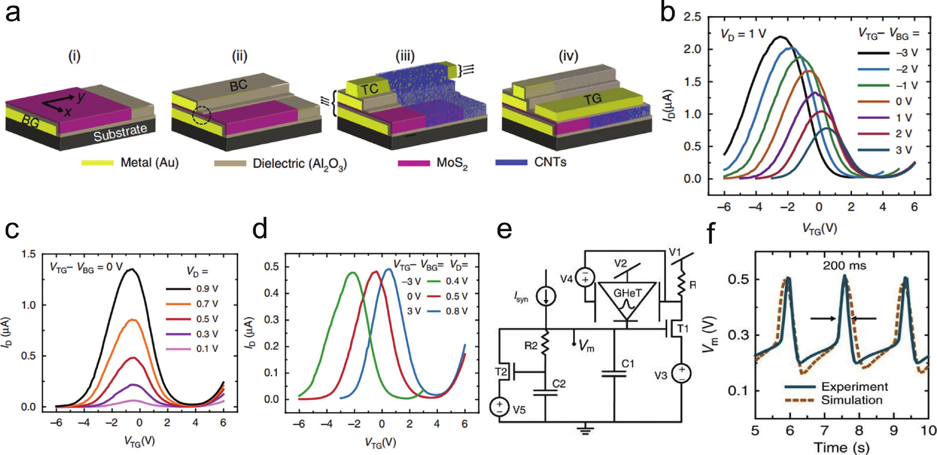
Fig. 8.  (Color online) Spiking neuron based on 2D reconfigurable Gaussian heterojunction transistor (GHeT). (a) The fabrication process of the dual-gated GHeT based on SWCNTs/MoS2 heterojunction. IDVTG characteristics of the GHeT shows the control of (b) both sides of the anti-ambipolar response and of the peak position, (c) the height and (d) the peak position. (e) The diagram of the spiking neuron circuit that utilizing only one GHeT. (f) The experiment and simulation results of the GHeT spiking neuron exhibit spiking and resetting behaviors[31].

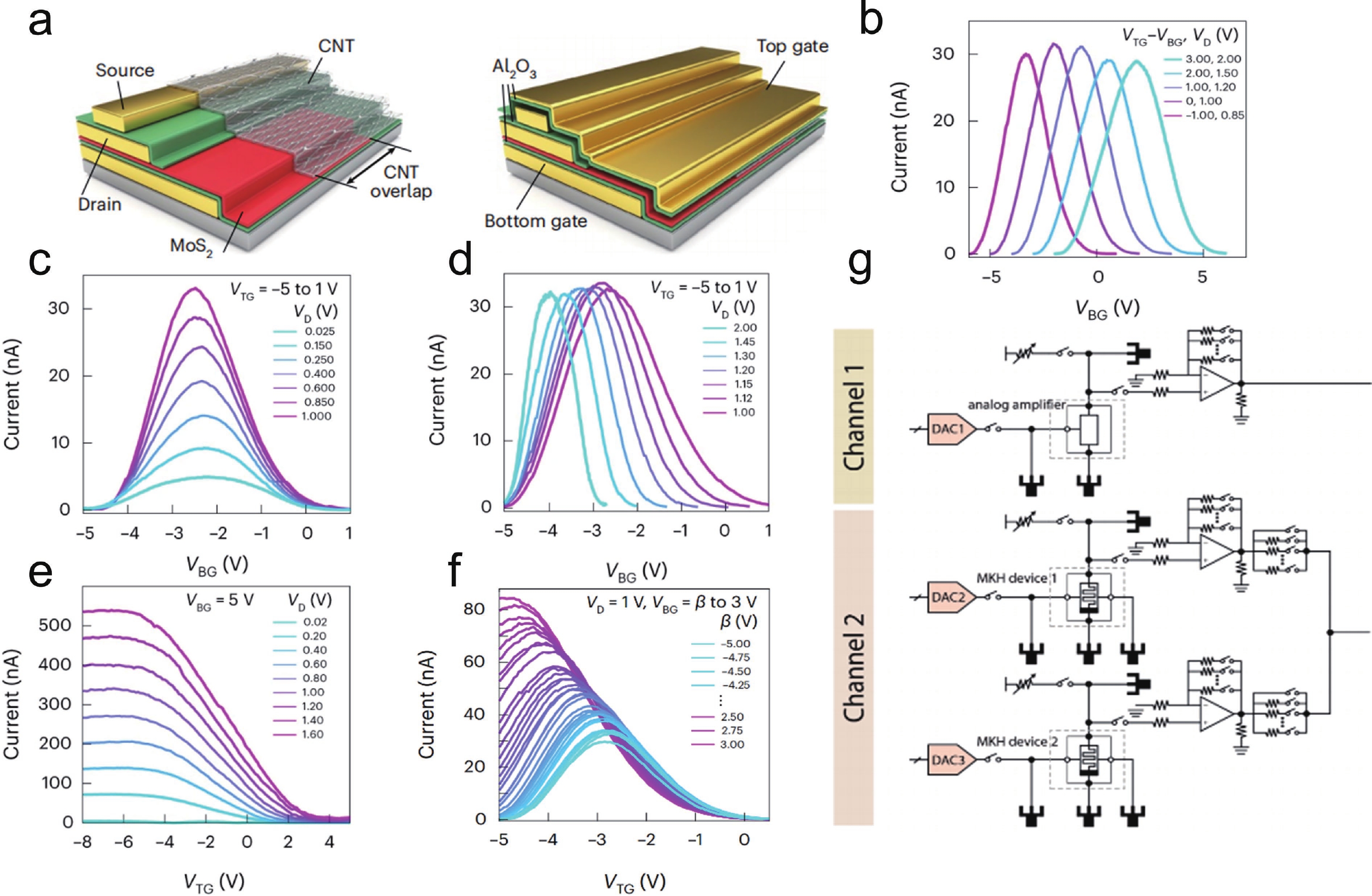
Fig. 9.  (Color online) AI hardware implementations based on 2D reconfigurable mixed-kernel heterojunction (MKH) transistors. (a) The schematic of the MKH transistor based on MoS2/CNT heterojunction. (b) The mean, (c) amplitude, and (d) standard deviation of the Gaussian function in IDVBG curves can be individually controlled by the VTG. (e) The tunable sigmoid function shown in the IDVTG curves. (f) IDVTG curves of the MKH transistor exhibit both Gaussian and sigmoid characteristics with a tunable mixing ratio under different bias configuration of VBG. (g) The circuit of the hardware implementation of a mixed-kernel support vector machine classification for arrhythmia detection, which only consists two MKH transistors[99].

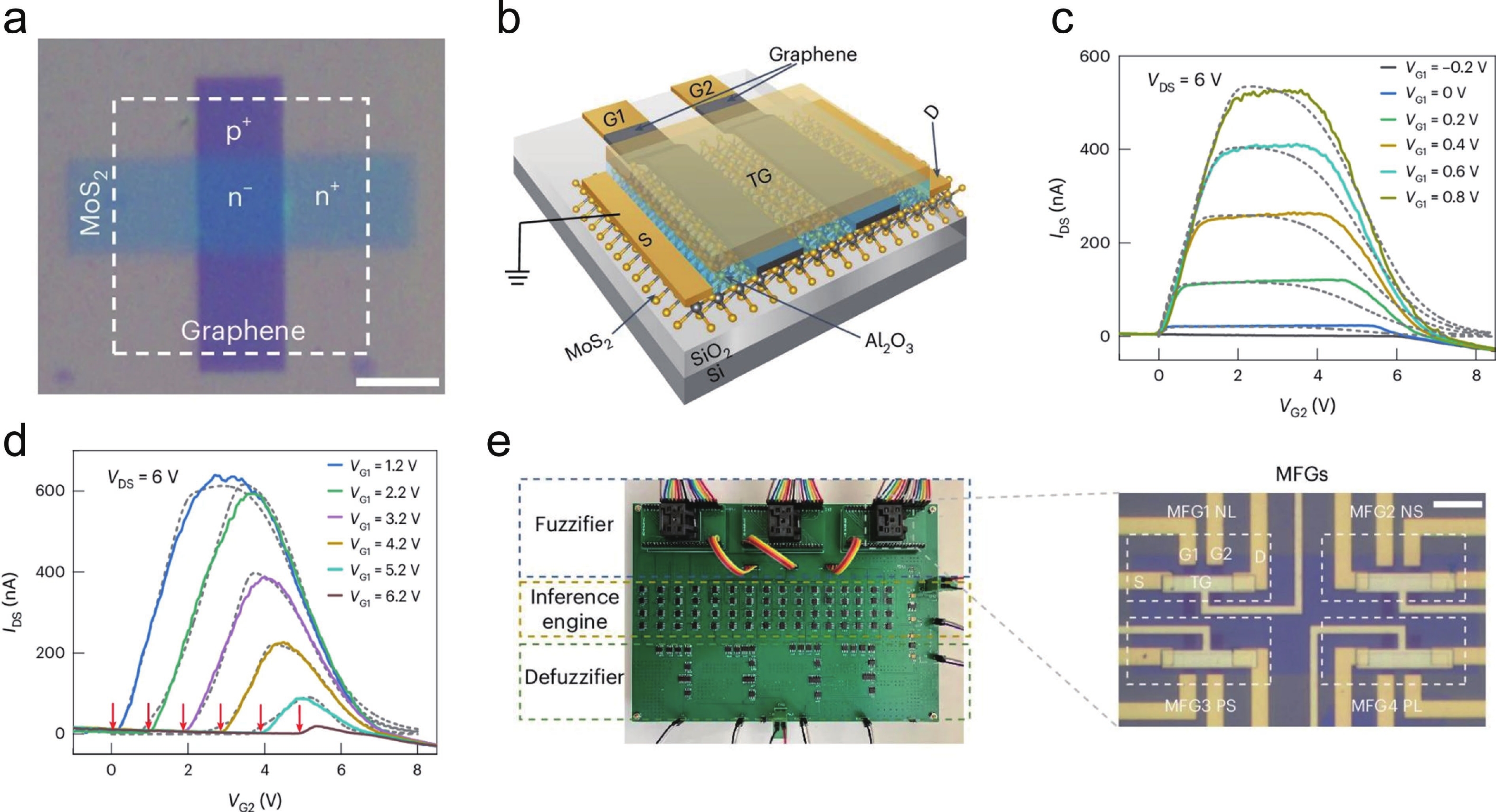
Fig. 10.  (Color online) An FLS hardware based on the multi-gate van der Waals interfacial junction transistor (vdW-IJT). (a) Optical image of the lateral MoS2/graphene junction. (b) Schematic of the multi-gate vdW-IJT with G1, G2, and a global top gate (TG). IDSVG2 curves of the multi-gate vdW-IJT showing (c) π-shape and (d) Gaussian-like shape membership functions. (e) The image of a complete FLS hardware on a PCB (left) and detailed image of four membership function generators in a chip (right) [30].

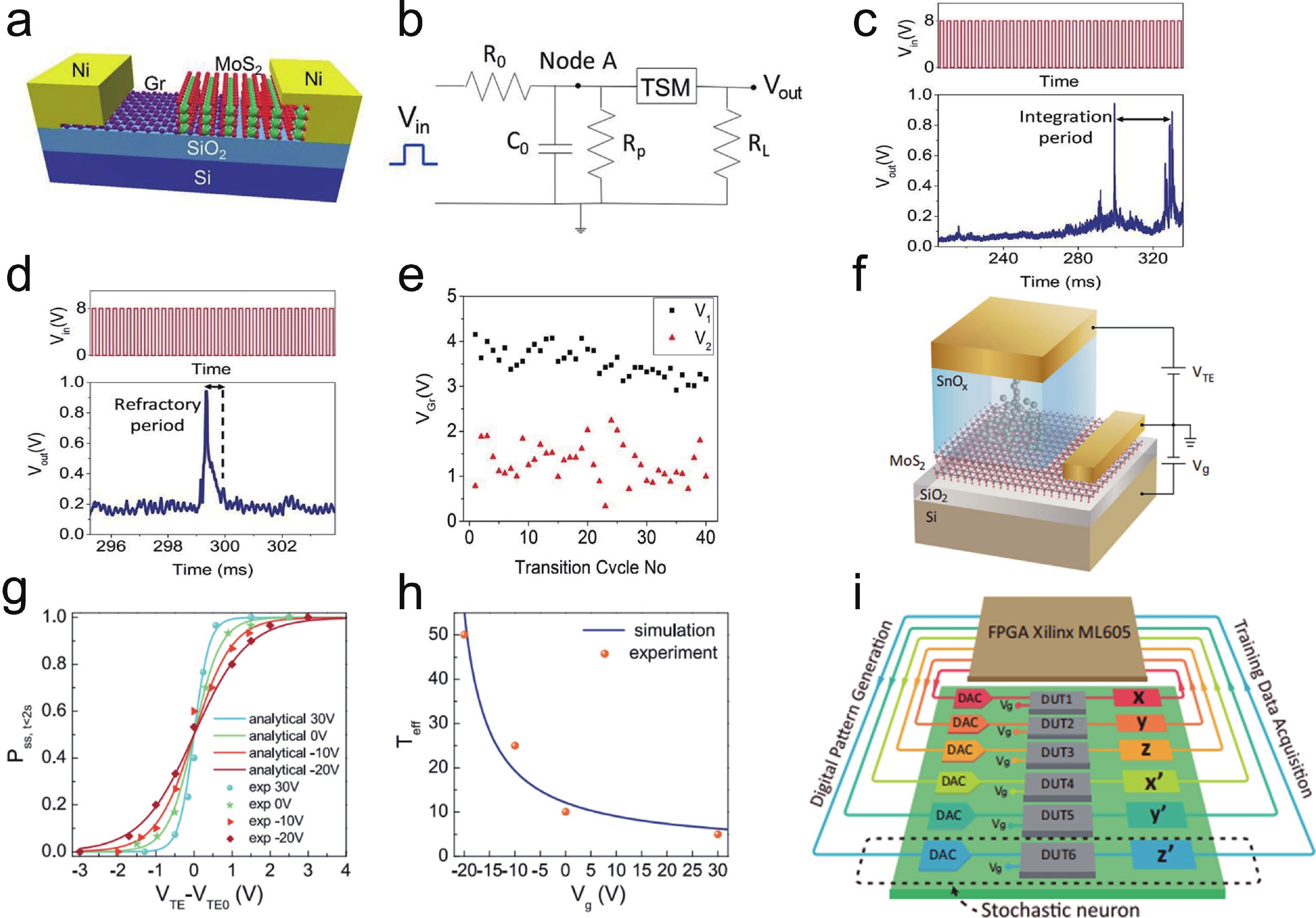
Fig. 11.  (Color online) AI hardware implementations based on 2D reconfigurable memristors. (a) The schematic of the threshold-switching memristor based on the vertical MoS2/graphene vdWH. (b) The circuit of the artificial neuron based on only one threshold-switching memristor. The output spikes of the artificial neuron circuit that exhibiting (c) integration period and (d) refractory period. (e) The stochastic distribution characteristics of V1 and V2 by repeating the switch of HRS/LRS[116]. (f) The schematic of the three-terminal stochastic memristor based on SnOx/MoS2 heterostructure. (g) The Pss,t<2s− (VTEVTE0) curves of the stochastic memristor show exponential-class sigmoidal distributions. (h) The relationship of the effective "temperature" (Teff) and Vg. (i) The schematic of the Boltzmann machine circuit where each stochastic neuron consists only one stochastic memristor and a simple peripheral circuit[25].

Table 1.   The comparison between 2D reconfigurable device and traditional CMOS transistor.

Comparison 2D reconfigurable device Traditional CMOS transistor
Polarity(n or p type) Polarity-switchable according to external conditions Polarity is decided by doping process and is fixed
Electronical properties Flexible and tunable Relatively fixed field-effect
Multifunction Multifunctional in a single device Limited by fixed electronical properties
Short channel effect Immune to short channel effect Limited by short channel effect
Performance High performance (on/off current ratio, tunability) and low power consumption Limited by leakage current, large footprint and
high power consumption
DownLoad: CSV
[1]
Loubet N, Hook T, Montanini P, et al. Stacked nanosheet gate-all-around transistor to enable scaling beyond FinFET. 2017 Symposium on VLSI Technology, 2017, T230 doi: 10.23919/VLSIT.2017.7998183
[2]
Bravaix A, Hamparsoumian G, Sonzogni J, et al. CMOS scaling challenges for high performance and low power applications facing reliability criteria towards the decananometer range. J Phys: Conf Ser, 2023, 2548(1), 012003 doi: 10.1088/1742-6596/2548/1/012003
[3]
Radamson H H, He X B, Zhang Q Z, et al. Miniaturization of cmos. Micromachines, 2019, 10(5), 293 doi: 10.3390/mi10050293
[4]
Yin L, Cheng R Q, Wen Y, et al. Emerging 2D memory devices for in-memory computing. Adv Mater, 2021, 33(29), e2007081 doi: 10.1002/adma.202007081
[5]
Lee H E, Park J H, Kim T J, et al. Novel electronics for flexible and neuromorphic computing. Adv Funct Materials, 2018, 28(32), 1801690 doi: 10.1002/adfm.201801690
[6]
Heinzig A, Pregl S, Trommer J, et al. Reconfigurable NAND-NOR circuits fabricated by a CMOS printing technique. 2017 IEEE 12th Nanotechnology Materials and Devices Conference (NMDC), 2017, 179 doi: 10.1109/NMDC.2017.8350546
[7]
Peng R X, Wu Y H, Wang B L, et al. Programmable graded doping for reconfigurable molybdenum ditelluride devices. Nat Electron, 2023, 6, 852 doi: 10.1038/s41928-023-01056-1
[8]
Shingaya Y, Zulkefli A, Iwasaki T, et al. Dual-gate anti-ambipolar transistor with van der Waals ReS2/WSe2 heterojunction for reconfigurable logic operations. Adv Elect Materials, 2023, 9(1), 2200704 doi: 10.1002/aelm.202200704
[9]
Novoselov K S, Geim A K, Morozov S V, et al. Electric field effect in atomically thin carbon films. Science, 2004, 306(5696), 666 doi: 10.1126/science.1102896
[10]
Feng C Y, Wu W W, Liu H D, et al. Emerging opportunities for 2D materials in neuromorphic computing. Nanomaterials, 2023, 13(19), 2720 doi: 10.3390/nano13192720
[11]
Liu Y, Weiss N O, Duan X D, et al. Van der Waals heterostructures and devices. Nat Rev Mater, 2016, 1(9), 16042 doi: 10.1038/natrevmats.2016.42
[12]
Lemme M C, Akinwande D, Huyghebaert C, et al. 2D materials for future heterogeneous electronics. Nat Commun, 2022, 13(1), 1392 doi: 10.1038/s41467-022-29001-4
[13]
Liu C S, Chen H W, Wang S Y, et al. Two-dimensional materials for next-generation computing technologies. Nat Nanotechnol, 2020, 15(7), 545 doi: 10.1038/s41565-020-0724-3
[14]
Lukman S, Ding L, Xu L, et al. High oscillator strength interlayer excitons in two-dimensional heterostructures for mid-infrared photodetection. Nat Nanotechnol, 2020, 15(8), 675 doi: 10.1038/s41565-020-0717-2
[15]
Ye X L, Du Y N, Wang M Y, et al. Advances in the field of two-dimensional crystal-based photodetectors. Nanomaterials, 2023, 13(8), 1379 doi: 10.3390/nano13081379
[16]
Liu C Y, Guo J S, Yu L W, et al. Silicon/2D-material photodetectors: From near-infrared to mid-infrared. Light Sci Appl, 2021, 10(1), 123 doi: 10.1038/s41377-021-00551-4
[17]
Liu Z J, Gong X G, Cheng J R, et al. Wafer-scale synthesis of two-dimensional materials for integrated electronics. Chip, 2024, 3(1), 100080 doi: 10.1016/j.chip.2023.100080
[18]
Zhang L N, Dong J C, Ding F. Strategies, status, and challenges in wafer scale single crystalline two-dimensional materials synthesis. Chem Rev, 2021, 121(11), 6321 doi: 10.1021/acs.chemrev.0c01191
[19]
Chen T A, Chuu C P, Tseng C C, et al. Wafer-scale single-crystal hexagonal boron nitride monolayers on Cu (111). Nature, 2020, 579(7798), 219 doi: 10.1038/s41586-020-2009-2
[20]
Yang P F, Zhang S Q, Pan S Y, et al. Epitaxial growth of centimeter-scale single-crystal MoS2 monolayer on Au(111). ACS Nano, 2020, 14(4), 5036 doi: 10.1021/acsnano.0c01478
[21]
Fei W W, Trommer J, Lemme M C, et al. Emerging reconfigurable electronic devices based on two-dimensional materials: A review. InfoMat, 2022, 4(10), e12355 doi: 10.1002/inf2.12355
[22]
Mir S H, Yadav V K, Singh J K. Recent advances in the carrier mobility of two-dimensional materials: A theoretical perspective. ACS Omega, 2020, 5(24), 14203 doi: 10.1021/acsomega.0c01676
[23]
Gomes F O V, Pokle A, Marinkovic M, et al. High mobility solution processed MoS2 thin film transistors. Solid State Electron, 2019, 158, 75 doi: 10.1016/j.sse.2019.05.011
[24]
Cao W, Chu J H, Parto K, et al. A mode-balanced reconfigurable logic gate built in a van der Waals strata. NPJ 2D Mater Appl, 2021, 5, 20 doi: 10.1038/s41699-020-00198-6
[25]
Yan X D, Ma J H, Wu T, et al. Reconfigurable Stochastic neurons based on tin oxide/MoS2 hetero-memristors for simulated annealing and the Boltzmann machine. Nat Commun, 2021, 12, 5710 doi: 10.1038/s41467-021-26012-5
[26]
Chaves A, Azadani J G, Alsalman H, et al. Bandgap engineering of two-dimensional semiconductor materials. NPJ 2D Mater Appl, 2020, 4, 29 doi: 10.1038/s41699-020-00162-4
[27]
Jung D Y, Yang S Y, Park H, et al. Interface engineering for high performance graphene electronic devices. Nano Convergence, 2015, 2(1), 11 doi: 10.1186/s40580-015-0042-x
[28]
Sangwan V K, Beck M E, Henning A, et al. Self-aligned van der Waals heterojunction diodes and transistors. Nano Lett, 2018, 18(2), 1421 doi: 10.1021/acs.nanolett.7b05177
[29]
Xiong X, Kang J Y, Hu Q L, et al. Reconfigurable logic-in-memory and multilingual artificial synapses based on 2D heterostructures. Adv Funct Materials, 2020, 30(11), 1909645 doi: 10.1002/adfm.201909645
[30]
Liu H F, Wu J B, Ma J H, et al. A van der Waals interfacial junction transistor for reconfigurable fuzzy logic hardware. Nat Electron, 2024, 7, 876 doi: 10.1038/s41928-024-01256-3
[31]
Beck M E, Shylendra A, Sangwan V K, et al. Spiking neurons from tunable Gaussian heterojunction transistors. Nat Commun, 2020, 11(1), 1565 doi: 10.1038/s41467-020-15378-7
[32]
Meng Y, Wang W, Wang W, et al. Anti-ambipolar heterojunctions: Materials, devices, and circuits. Adv Mater, 2024, 36(17), e2306290 doi: 10.1002/adma.202306290
[33]
Chhowalla M, Jena D, Zhang H. Two-dimensional semiconductors for transistors. Nat Rev Mater, 2016, 1(11), 16052 doi: 10.1038/natrevmats.2016.52
[34]
Li H, Ling J Y, Lin J M, et al. Interface engineering in two-dimensional heterostructures towards novel emitters. J Semicond, 2023, 44(1), 011001 doi: 10.1088/1674-4926/44/1/011001
[35]
Wang H Y, Song X Y, Li Z X, et al. Recent advances in two-dimensional photovoltaic devices. J Semicond, 2024, 45(5), 051701 doi: 10.1088/1674-4926/45/5/051701
[36]
Thakar K, Lodha S. Multi-bit analog transmission enabled by electrostatically reconfigurable ambipolar and anti-ambipolar transport. ACS Nano, 2021, 15(12), 19692 doi: 10.1021/acsnano.1c07032
[37]
Jariwala D, Sangwan V K, Wu C C, et al. Gate-tunable carbon nanotube-MoS2 heterojunction p-n diode. Proc Natl Acad Sci USA, 2013, 110(45), 18076 doi: 10.1073/pnas.1317226110
[38]
Nourbakhsh A, Zubair A, Dresselhaus M S, et al. Transport properties of a MoS2/WSe2 heterojunction transistor and its potential for application. Nano Lett, 2016, 16(2), 1359 doi: 10.1021/acs.nanolett.5b04791
[39]
Roy T, Tosun M, Cao X, et al. Dual-gated MoS2/WSe2 van der Waals tunnel diodes and transistors. ACS Nano, 2015, 9(2), 2071 doi: 10.1021/nn507278b
[40]
Huo N J, Yang J H, Huang L, et al. Tunable polarity behavior and self-driven photoswitching in p-WSe2/n-WS2 heterojunctions. Small, 2015, 11(40), 5430 doi: 10.1002/smll.201501206
[41]
Huang M Q, Li S M, Zhang Z F, et al. Multifunctional high-performance van der Waals heterostructures. Nat Nanotechnol, 2017, 12(12), 1148 doi: 10.1038/nnano.2017.208
[42]
Li Y T, Wang Y, Huang L, et al. Anti-ambipolar field-effect transistors based on few-layer 2D transition metal dichalcogenides. ACS Appl Mater Interfaces, 2016, 8(24), 15574 doi: 10.1021/acsami.6b02513
[43]
Yan R S, Fathipour S, Han Y M, et al. Esaki diodes in van der Waals heterojunctions with broken-gap energy band alignment. Nano Lett, 2015, 15(9), 5791 doi: 10.1021/acs.nanolett.5b01792
[44]
Hayakawa R, Takahashi K, Zhong X H, et al. Reconfigurable logic-in-memory constructed using an organic antiambipolar transistor. Nano Lett, 2023, 23(17), 8339 doi: 10.1021/acs.nanolett.3c02726
[45]
Kobashi K, Hayakawa R, Chikyow T, et al. Multi-valued logic circuits based on organic anti-ambipolar transistors. Nano Lett, 2018, 18(7), 4355 doi: 10.1021/acs.nanolett.8b01357
[46]
Shim J, Oh S, Kang D H, et al. Phosphorene/rhenium disulfide heterojunction-based negative differential resistance device for multi-valued logic. Nat Commun, 2016, 7, 13413 doi: 10.1038/ncomms13413
[47]
Maeda K, Okabayashi N, Kano S, et al. Logic operations of chemically assembled single-electron transistor. ACS Nano, 2012, 6(3), 2798 doi: 10.1021/nn3003086
[48]
Wakayama Y, Hayakawa R. Antiambipolar transistor: A newcomer for future flexible electronics. Adv Funct Materials, 2020, 30(20), 1903724 doi: 10.1002/adfm.201903724
[49]
Yoo H, Kim C H. Multi-valued logic system: New opportunities from emerging materials and devices. J Mater Chem C, 2021, 9(12), 4092 doi: 10.1039/D1TC00148E
[50]
Kim C H, Hayakawa R, Wakayama Y. Fundamentals of organic anti-ambipolar ternary inverters. Adv Elect Materials, 2020, 6(3), 1901200 doi: 10.1002/aelm.201901200
[51]
Kim J B, Li J S, Choi Y, et al. Photosensitive graphene P-N junction transistors and ternary inverters. ACS Appl Mater Interfaces, 2018, 10(15), 12897 doi: 10.1021/acsami.8b00483
[52]
Wu E X, Xie Y, Liu Q Z, et al. Photoinduced doping to enable tunable and high-performance anti-ambipolar MoTe2/MoS2 heterotransistors. ACS Nano, 2019, 13(5), 5430 doi: 10.1021/acsnano.9b00201
[53]
Lim J H, Shim J, Kang B S, et al. Double negative differential transconductance characteristic: From device to circuit application toward quaternary inverter. Adv Funct Materials, 2019, 29(48), 1905540 doi: 10.1002/adfm.201905540
[54]
Jung K S, Heo K, Kim M J, et al. Double negative differential resistance device based on hafnium disulfide/pentacene hybrid structure. Adv Sci, 2020, 7(19), 2000991 doi: 10.1002/advs.202000991
[55]
Kim K H, Park H Y, Shim J, et al. A multiple negative differential resistance heterojunction device and its circuit application to ternary static random access memory. Nanoscale Horiz, 2020, 5(4), 654 doi: 10.1039/C9NH00631A
[56]
Yang B H, Chen J, Tu F B. Towards efficient generative AI and beyond-AI computing: New trends on ISSCC 2024 machine learning accelerators. J Semicond, 2024, 45(4), 040204 doi: 10.1088/1674-4926/45/4/040204
[57]
Zou X Q, Xu S, Chen X M, et al. Breaking the von Neumann bottleneck: Architecture-level processing-in-memory technology. Sci China Inf Sci, 2021, 64(6), 160404 doi: 10.1007/s11432-020-3227-1
[58]
Sasaki T, Ueno K, Taniguchi T, et al. Material and device structure designs for 2D memory devices based on the floating gate voltage trajectory. ACS Nano, 2021, 15(4), 6658 doi: 10.1021/acsnano.0c10005
[59]
Bertolazzi S, Bondavalli P, Roche S, et al. Nonvolatile memories based on graphene and related 2D materials. Adv Mater, 2019, 31(10), e1806663 doi: 10.1002/adma.201806663
[60]
Seo S, Lee J J, Lee H J, et al. Recent progress in artificial synapses based on two-dimensional van der Waals materials for brain-inspired computing. ACS Appl Electron Mater, 2020, 2(2), 371 doi: 10.1021/acsaelm.9b00694
[61]
Li D, Chen M Y, Sun Z Z, et al. Two-dimensional non-volatile programmable p-n junctions. Nat Nanotechnol, 2017, 12(9), 901 doi: 10.1038/nnano.2017.104
[62]
Yin L, Wang F, Cheng R Q, et al. Van der Waals heterostructure devices with dynamically controlled conduction polarity and multifunctionality. Adv Funct Materials, 2019, 29(1), 1804897 doi: 10.1002/adfm.201804897
[63]
Xiong X, Kang J Y, Liu S Y, et al. Nonvolatile logic and ternary content-addressable memory based on complementary black phosphorus and rhenium disulfide transistors. Adv Mater, 2022, 34(48), e2106321 doi: 10.1002/adma.202106321
[64]
Kumar A, Giubileo F, Sleziona S, et al. Temperature dependent black phosphorus transistor and memory. Nano Ex, 2023, 4(1), 014001 doi: 10.1088/2632-959X/acbe11
[65]
Liu L, Liu C S, Jiang L L, et al. Ultrafast non-volatile flash memory based on van der Waals heterostructures. Nat Nanotechnol, 2021, 16(8), 874 doi: 10.1038/s41565-021-00921-4
[66]
Hou X, Yan X, Liu C S, et al. Operation mode switchable charge-trap memory based on few-layer MoS2. Semicond Sci Technol, 2018, 33(3), 034001 doi: 10.1088/1361-6641/aaa79e
[67]
Zhang E Z, Wang W Y, Zhang C, et al. Tunable charge-trap memory based on few-layer MoS2. ACS Nano, 2015, 9(1), 612 doi: 10.1021/nn5059419
[68]
Zhang P F, Li D, Chen M Y, et al. Floating-gate controlled programmable non-volatile black phosphorus PNP junction memory. Nanoscale, 2018, 10(7), 3148 doi: 10.1039/C7NR08515J
[69]
Vu Q A, Shin Y S, Kim Y R, et al. Two-terminal floating-gate memory with van der Waals heterostructures for ultrahigh on/off ratio. Nat Commun, 2016, 7, 12725 doi: 10.1038/ncomms12725
[70]
Luo Z D, Zhang S Q, Liu Y, et al. Dual-ferroelectric-coupling-engineered two-dimensional transistors for multifunctional in-memory computing. ACS Nano, 2022, 16(2), 3362 doi: 10.1021/acsnano.2c00079
[71]
Sheng Z, Dong J G, Hu W N, et al. Reconfigurable logic-in-memory computing based on a polarity-controllable two-dimensional transistor. Nano Lett, 2023, 23(11), 5242 doi: 10.1021/acs.nanolett.3c01248
[72]
Sun X X, Zhu C G, Yi J L, et al. Reconfigurable logic-in-memory architectures based on a two-dimensional van der Waals heterostructure device. Nat Electron, 2022, 5, 752 doi: 10.1038/s41928-022-00858-z
[73]
Zhao Z J, Rakheja S, Zhu W J. Nonvolatile reconfigurable 2D Schottky barrier transistors. Nano Lett, 2021, 21(21), 9318 doi: 10.1021/acs.nanolett.1c03557
[74]
Seo S Y, Moon G, Okello O F N, et al. Reconfigurable photo-induced doping of two-dimensional van der Waals semiconductors using different photon energies. Nat Electron, 2021, 4, 38 doi: 10.1038/s41928-020-00512-6
[75]
Migliato Marega G, Zhao Y F, Avsar A, et al. Logic-in-memory based on an atomically thin semiconductor. Nature, 2020, 587(7832), 72 doi: 10.1038/s41586-020-2861-0
[76]
Hou X, Liu C S, Ding Y, et al. A logic-memory transistor with the integration of visible information sensing-memory-processing. Adv Sci, 2020, 7(21), 2002072 doi: 10.1002/advs.202002072
[77]
Cheng R Q, Wang F, Yin L, et al. High-performance, multifunctional devices based on asymmetric van der Waals heterostructures. Nat Electron, 2018, 1, 356 doi: 10.1038/s41928-018-0086-0
[78]
Yap W C, Jiang H, Liu J L, et al. Ferroelectric transistors with monolayer molybdenum disulfide and ultra-thin aluminum-doped hafnium oxide. Appl Phys Lett , 2017, 111(1), 013103 doi: 10.1063/1.4991877
[79]
Shekhawat A, Walters G, Yang N, et al. Data retention and low voltage operation of Al2O3/Hf0.5Zr0.5O2 based ferroelectric tunnel junctions. Nanotechnology, 2020, 31(39), 39LT01 doi: 10.1088/1361-6528/ab9cf7
[80]
Zhao R T, Zhao X Y, Liu H F, et al. Reconfigurable logic-memory hybrid device based on ferroelectric Hf0.5Zr0.5O2. IEEE Electron Device Lett, 2021, 42(8), 1164 doi: 10.1109/LED.2021.3089326
[81]
Lv L, Zhuge F W, Xie F J, et al. Reconfigurable two-dimensional optoelectronic devices enabled by local ferroelectric polarization. Nat Commun, 2019, 10(1), 3331 doi: 10.1038/s41467-019-11328-0
[82]
Zhu C C, Wang Y R, Wang F, et al. Nonvolatile reconfigurable broadband photodiodes based on BP/α-In2Se3 ferroelectric p–n junctions. Appl Phys Lett, 2022, 120(8), 083101 doi: 10.1063/5.0079535
[83]
Chen L, Wang T Y, Dai Y W, et al. Ultra-low power Hf0.5Zr0.5O2 based ferroelectric tunnel junction synapses for hardware neural network applications. Nanoscale, 2018, 10(33), 15826 doi: 10.1039/C8NR04734K
[84]
Wang Y R, Wang F, Wang Z X, et al. Reconfigurable photovoltaic effect for optoelectronic artificial synapse based on ferroelectric p-n junction. Nano Res, 2021, 14(11), 4328 doi: 10.1007/s12274-021-3833-x
[85]
Tsai M Y, Huang C T, Lin C Y, et al. A reconfigurable transistor and memory based on a two-dimensional heterostructure and photoinduced trapping. Nat Electron, 2023, 6, 755 doi: 10.1038/s41928-023-01034-7
[86]
Bae J H, Kim H, Kwon D, et al. Reconfigurable field-effect transistor as a synaptic device for XNOR binary neural network. IEEE Electron Device Lett, 2019, 40(4), 624 doi: 10.1109/LED.2019.2898448
[87]
Yin L, Cheng R Q, Wang Z X, et al. Two-dimensional unipolar memristors with logic and memory functions. Nano Lett, 2020, 20(6), 4144 doi: 10.1021/acs.nanolett.0c00002
[88]
Liu C S, Chen H W, Hou X, et al. Small footprint transistor architecture for photoswitching logic and in situ memory. Nat Nanotechnol, 2019, 14(7), 662 doi: 10.1038/s41565-019-0462-6
[89]
Liu C S, Yan X, Song X F, et al. A semi-floating gate memory based on van der Waals heterostructures for quasi-non-volatile applications. Nat Nanotechnol, 2018, 13(5), 404 doi: 10.1038/s41565-018-0102-6
[90]
Li J Y, Zhang H, Ding Y, et al. A non-volatile AND gate based on Al2O3/HfO2/Al2O3 charge-trap stack for in situ storage applications. Sci Bull, 2019, 64(20), 1518 doi: 10.1016/j.scib.2019.08.012
[91]
Zhang X H, Peng B. The twisted two-dimensional ferroelectrics. J Semicond, 2023, 44(1), 011002 doi: 10.1088/1674-4926/44/1/011002
[92]
Yao H, Wu E X, Liu J. Frequency doubler based on a single MoTe2/MoS2 anti-ambipolar heterostructure. Appl Phys Lett, 2020, 117(12), 1231, 03 doi: 10.1063/5.0018882
[93]
Lee M, Kim T W, Park C Y, et al. Graphene bridge heterostructure devices for negative differential transconductance circuit applications. Nanomicro Lett, 2022, 15(1), 22 doi: 10.1007/s40820-022-01001-5
[94]
Yuce M R, Liu W T. A low-power multirate differential PSK receiver for space applications. IEEE Trans Veh Technol, 2005, 54(6), 2074 doi: 10.1109/TVT.2005.858196
[95]
Das S, Das S. Digital keying enabled by reconfigurable 2D modulators. Adv Mater, 2022, 34(43), e2203753 doi: 10.1002/adma.202203753
[96]
Jariwala D, Sangwan V K, Seo J T, et al. Large-area, low-voltage, antiambipolar heterojunctions from solution-processed semiconductors. Nano Lett, 2015, 15(1), 416 doi: 10.1021/nl5037484
[97]
Crespo J L, Duro R J, Pena F L. Gaussian synapse ANNs in multi- and hyperspectral image data analysis. IEEE Trans Instrum Meas, 2003, 52(3), 724 doi: 10.1109/TIM.2003.814693
[98]
Sebastian A, Pannone A, Subbulakshmi Radhakrishnan S, et al. Gaussian synapses for probabilistic neural networks. Nat Commun, 2019, 10(1), 4199 doi: 10.1038/s41467-019-12035-6
[99]
Yan X D, Qian J H, Ma J H, et al. Reconfigurable mixed-kernel heterojunction transistors for personalized support vector machine classification. Nat Electron, 2023, 6, 862 doi: 10.1038/s41928-023-01042-7
[100]
Sangwan V K, Hersam M C. Neuromorphic nanoelectronic materials. Nat Nanotechnol, 2020, 15(7), 517 doi: 10.1038/s41565-020-0647-z
[101]
Maass W. Networks of spiking neurons: The third generation of neural network models. Neural Netw, 1997, 10(9), 1659 doi: 10.1016/S0893-6080(97)00011-7
[102]
Gao L G, Chen P Y, Yu S M. NbOx based oscillation neuron for neuromorphic computing. Appl Phys Lett, 2017, 111(10), 103503 doi: 10.1063/1.4991917
[103]
Wang J Y, Teng C J, Zhang Z Y, et al. A scalable artificial neuron based on ultrathin two-dimensional titanium oxide. ACS Nano, 2021, 15(9), 15123 doi: 10.1021/acsnano.1c05565
[104]
Wang Z R, Joshi S, Savel’ev S, et al. Fully memristive neural networks for pattern classification with unsupervised learning. Nat Electron, 2018, 1, 137 doi: 10.1038/s41928-018-0023-2
[105]
Wang Z, Crafton B, Gomez J, et al. Experimental demonstration of ferroelectric spiking neurons for unsupervised clustering. 2018 IEEE International Electron Devices Meeting (IEDM), 2018, 13.3.1 doi: 10.1109/IEDM.2018.8614586
[106]
Sangwan V K, Jariwala D, Kim I S, et al. Gate-tunable memristive phenomena mediated by grain boundaries in single-layer MoS2. Nat Nanotechnol, 2015, 10(5), 403 doi: 10.1038/nnano.2015.56
[107]
Wang M, Cai S H, Pan C, et al. Robust memristors based on layered two-dimensional materials. Nat Electron, 2018, 1, 130 doi: 10.1038/s41928-018-0021-4
[108]
Shi Y Y, Liang X H, Yuan B, et al. Electronic synapses made of layered two-dimensional materials. Nat Electron, 2018, 1, 458 doi: 10.1038/s41928-018-0118-9
[109]
Sun L F, Hwang G, Choi W, et al. Ultralow switching voltage slope based on two-dimensional materials for integrated memory and neuromorphic applications. Nano Energy, 2020, 69, 104472 doi: 10.1016/j.nanoen.2020.104472
[110]
Zhu X J, Li D, Liang X G, et al. Ionic modulation and ionic coupling effects in MoS2 devices for neuromorphic computing. Nat Mater, 2019, 18(2), 141 doi: 10.1038/s41563-018-0248-5
[111]
Zhang F, Zhang H R, Krylyuk S, et al. Electric-field induced structural transition in vertical MoTe2- and Mo1- xW xTe2-based resistive memories. Nat Mater, 2019, 18(1), 55 doi: 10.1038/s41563-018-0234-y
[112]
Feng X W, Li Y D, Wang L, et al. A fully printed flexible MoS2 memristive artificial synapse with femtojoule switching energy. Adv Elect Mater, 2019, 5(12), 1900740 doi: 10.1002/aelm.201900740
[113]
Wang K Y, Li L T, Zhao R J, et al. A pure 2H-MoS2 nanosheet-based memristor with low power consumption and linear multilevel storage for artificial synapse emulator. Adv Elect Mater, 2020, 6(3), 1901342 doi: 10.1002/aelm.201901342
[114]
Cai F X, Kumar S, Van Vaerenbergh T, et al. Power-efficient combinatorial optimization using intrinsic noise in memristor Hopfield neural networks. Nat Electron, 2020, 3, 409 doi: 10.1038/s41928-020-0436-6
[115]
Jiang H, Belkin D, Savel’ev S E, et al. A novel true random number generator based on a stochastic diffusive memristor. Nat Commun, 2017, 8(1), 882 doi: 10.1038/s41467-017-00869-x
[116]
Kalita H, Krishnaprasad A, Choudhary N, et al. Artificial neuron using vertical MoS2/graphene threshold switching memristors. Sci Rep, 2019, 9(1), 53 doi: 10.1038/s41598-018-35828-z
[117]
Bez R, Camerlenghi E, Modelli A, et al. Introduction to flash memory. Proc IEEE, 2003, 91(4), 489 doi: 10.1109/JPROC.2003.811702
[118]
Wang D, Zhang Z C, Li B, et al. Synthesis of two-dimensional/one-dimensional heterostructures with tunable width. J Semicond, 2021, 42(9), 092001 doi: 10.1088/1674-4926/42/9/092001
[119]
Zhao T G, Guo J X, Li T T, et al. Substrate engineering for wafer-scale two-dimensional material growth: Strategies, mechanisms, and perspectives. Chem Soc Rev, 2023, 52(5), 1650 doi: 10.1039/D2CS00657J
[120]
Quellmalz A, Wang X J, Sawallich S, et al. Large-area integration of two-dimensional materials and their heterostructures by wafer bonding. Nat Commun, 2021, 12(1), 917 doi: 10.1038/s41467-021-21136-0
[121]
Chen S C, Mahmoodi M R, Shi Y Y, et al. Wafer-scale integration of two-dimensional materials in high-density memristive crossbar arrays for artificial neural networks. Nat Electron, 2020, 3, 638 doi: 10.1038/s41928-020-00473-w
  • Search

    Advanced Search >>

    GET CITATION

    shu

    Export: BibTex EndNote

    Article Metrics

    Article views: 529 Times PDF downloads: 135 Times Cited by: 0 Times

    History

    Received: 29 November 2024 Revised: 17 January 2025 Online: Accepted Manuscript: 25 February 2025Uncorrected proof: 11 March 2025

    Catalog

      Email This Article

      User name:
      Email:*请输入正确邮箱
      Code:*验证码错误
      Liutianyi Zhang, Ping-Heng Tan, Jiangbin Wu. Reconfigurable devices based on two-dimensional materials for logic and analog applications[J]. Journal of Semiconductors, 2025, In Press. doi: 10.1088/1674-4926/24100005 ****L T Y Zhang, P H Tan, and J B Wu, Reconfigurable devices based on two-dimensional materials for logic and analog applications[J]. J. Semicond., 2025, 46(7), 071701 doi: 10.1088/1674-4926/24100005
      Citation:
      Liutianyi Zhang, Ping-Heng Tan, Jiangbin Wu. Reconfigurable devices based on two-dimensional materials for logic and analog applications[J]. Journal of Semiconductors, 2025, In Press. doi: 10.1088/1674-4926/24100005 ****
      L T Y Zhang, P H Tan, and J B Wu, Reconfigurable devices based on two-dimensional materials for logic and analog applications[J]. J. Semicond., 2025, 46(7), 071701 doi: 10.1088/1674-4926/24100005

      Reconfigurable devices based on two-dimensional materials for logic and analog applications

      DOI: 10.1088/1674-4926/24100005
      CSTR: 32376.14.1674-4926.24100005
      More Information
      • Liutianyi Zhang got his bachelor's degree in 2024 from Sichuan University majoring in Microelectronics Science and Engineering. Now he is a postgraduate student at the Institute of Semiconductors, University of Chinese Academy of Sciences, majoring in Microelectronics and solid-state Electronics. His main research interests include reconfigurable devices based on two-dimensional materials and their artificial intelligence hardware applications
      • Ping-Heng Tan is a professor at the Institute of Semiconductors Chinese Academy of Sciences. He obtained BS (1996) in Physics from Peking University and PhD (2001) from the Institute of Semiconductors, Chinese Academy of Sciences. He worked at Walter Schottky Institut, Technische Universitaet Muenchen as a Postdoc Research Associate from 2001−2003. He was a KC-Wong Royal Society Fellow at Cambridge University from 2006−2007. His current research is on two dimensional layered materials, nano carbon materials, topological insulators and novel low-dimensional semiconductor optoelectronic materials. He was supported by the National Science Fund for Distinguished Young Scholars in 2012
      • Jiangbin Wu is currently a professor at Institute of Semiconductors, Chinese Academy of Sciences. He graduated from the Department of Electronic Science and Technology of Huazhong University of Science and Technology in 2012. Jiang-Bin received his doctorate degree from the Institute of Semiconductors, Chinese Academy of Sciences in 2017 supervised by Prof. Ping-Heng Tan. He served as a postdoctoral fellow at the University of Southern California from 2017 to 2023. His research interest includes optical properties of emerging low-dimensional materials and semiconductor devices based on new low-dimensional materials
      • Corresponding author: phtan@semi.ac.cnjbwu@semi.ac.cn
      • Received Date: 2024-11-29
      • Revised Date: 2025-01-17
      • Available Online: 2025-02-25

      Catalog

        /

        DownLoad:  Full-Size Img  PowerPoint
        Return
        Return