| [1] |
Park S I, Xiong Y J, Kim R H, et al. Printed assemblies of inorganic light-emitting diodes for deformable and semitransparent displays. Science, 2009, 325(5943), 977 doi: 10.1126/science.1175690 |
| [2] |
|
| [3] |
Song Y M, Xie Y Z, Malyarchuk V, et al. Digital cameras with designs inspired by the arthropod eye. Nature, 2013, 497(7447), 95 doi: 10.1038/nature12083 |
| [4] |
Lu M, Zhang Y, Wang S X, et al. Metal halide perovskite light-emitting devices: Promising technology for next-generation displays. Adv Funct Mater, 2019, 29(30), 1902008 doi: 10.1002/adfm.201902008 |
| [5] |
Liashenko T G, Cherotchenko E D, Pushkarev A P, et al. Electronic structure of CsPbBr 3-xCl x perovskites: Synthesis, experimental characterization, and DFT simulations. Phys Chem Chem Phys, 2019, 21(35), 18930 doi: 10.1039/C9CP03656C |
| [6] |
Dey A, Ye J Z, De A, et al. State of the art and prospects for halide perovskite nanocrystals. ACS Nano, 2021, 15(7), 10775 doi: 10.1021/acsnano.0c08903 |
| [7] |
Amruth C, Luszczynska B, Rekab W, et al. Inkjet printing of an electron injection layer: New role of cesium carbonate interlayer in polymer OLEDs. Polymers, 2020, 13(1), 80 doi: 10.3390/polym13010080 |
| [8] |
Gustafsson G, Cao Y, Treacy G M, et al. Flexible light-emitting diodes made from soluble conducting polymers. Nature, 1992, 357, 477 doi: 10.1038/357477a0 |
| [9] |
Pietryga J M, Park Y S, Lim J, et al. Spectroscopic and device aspects of nanocrystal quantum dots. Chem Rev, 2016, 116(18), 10513 doi: 10.1021/acs.chemrev.6b00169 |
| [10] |
Kovalenko M V, Protesescu L, Bodnarchuk M I. Properties and potential optoelectronic applications of lead halide perovskite nanocrystals. Science, 2017, 358(6364), 745 doi: 10.1126/science.aam7093 |
| [11] |
Mohapatra A, Kar M R, Bhaumik S. Recent progress and prospects on metal halide perovskite nanocrystals as color converters in the fabrication of white light-emitting diodes. Front Electron Mater, 2022, 2, 891983 doi: 10.3389/femat.2022.891983 |
| [12] |
Zhao X F, De Andrew Ng J, Friend R H, et al. Opportunities and challenges in perovskite light-emitting devices. ACS Photonics, 2018, 5(10), 3866 doi: 10.1021/acsphotonics.8b00745 |
| [13] |
|
| [14] |
Zhang L X, Mei L Y, Wang K Y, et al. Advances in the application of perovskite materials. Nanomicro Lett, 2023, 15(1), 177 doi: 10.1007/s40820-023-01140-3 |
| [15] |
Gets D, Alahbakhshi M, Mishra A, et al. Reconfigurable perovskite LEC: Effects of ionic additives and dual function devices (advanced optical materials 3/2021). Adv Opt Mater, 2021, 9(3), 2170010 doi: 10.1002/adom.202170010 |
| [16] |
Cheng T, Zhang Y Z, Lai W Y, et al. Stretchable thin-film electrodes for flexible electronics with high deformability and stretchability. Adv Mater, 2015, 27(22), 3349 doi: 10.1002/adma.201405864 |
| [17] |
Miroshnichenko A S, Neplokh V, Mukhin I S, et al. Silicone materials for flexible optoelectronic devices. Materials, 2022, 15(24), 8731 doi: 10.3390/ma15248731 |
| [18] |
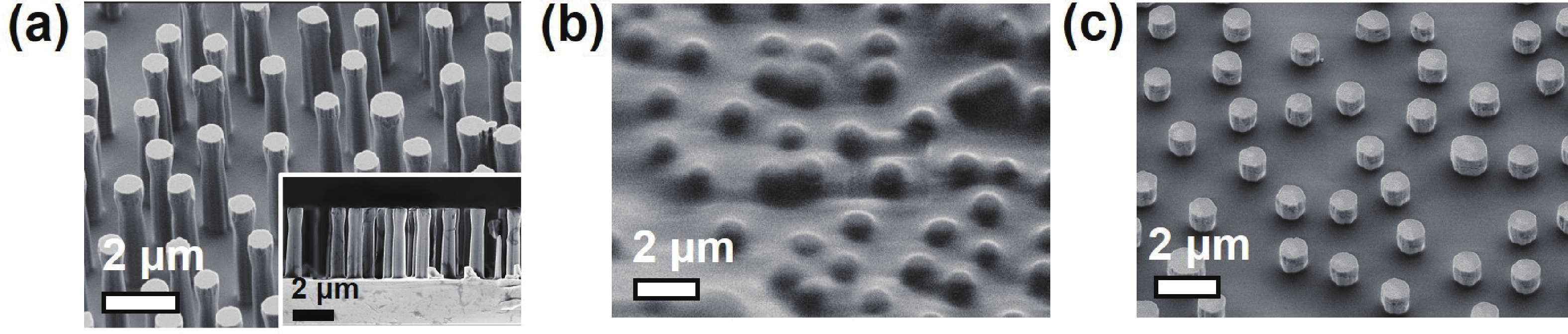
Bade S G R, Li J Q, Shan X, et al. Fully printed halide perovskite light-emitting diodes with silver nanowire electrodes. ACS Nano, 2016, 10(2), 1795 doi: 10.1021/acsnano.5b07506 |
| [19] |
Miroshnichenko A S, Deriabin K V, Baeva M, et al. Flexible perovskite CsPbBr 3 light emitting devices integrated with GaP nanowire arrays in highly transparent and durable functionalized silicones. J Phys Chem Lett, 2021, 12(39), 9672 doi: 10.1021/acs.jpclett.1c02611 |
| [20] |
Al-Ashouri A, Köhnen E, Li B, et al. Monolithic perovskite/silicon tandem solar cell with >29% efficiency by enhanced hole extraction. Science, 2020, 370(6522), 1300 doi: 10.1126/science.abd4016 |
| [21] |
Geng X S, Wang F W, Tian H, et al. Ultrafast photodetector by integrating perovskite directly on silicon wafer. ACS Nano, 2020, 14(3), 2860 doi: 10.1021/acsnano.9b06345 |
| [22] |
Wu T J, Pisula W, Rashid M Y A, et al. Application of perovskite-structured materials in field-effect transistors. Adv Elect Mater, 2019, 5(12), 1900444 doi: 10.1002/aelm.201900444 |
| [23] |
Rahimi F, Jafari A K, Hsu C A, et al. Selective sensing in perovskite-based image sensors. Org Electron, 2019, 75, 105397 doi: 10.1016/j.orgel.2019.105397 |
| [24] |
Yan M X, Tian H J, Yang D R, et al. Improved efficiency for silicon-based perovskite light-emitting diodes via interfacial hydrophilic modification. Adv Mater Inter, 2021, 8(21), 2101448 doi: 10.1002/admi.202101448 |
| [25] |
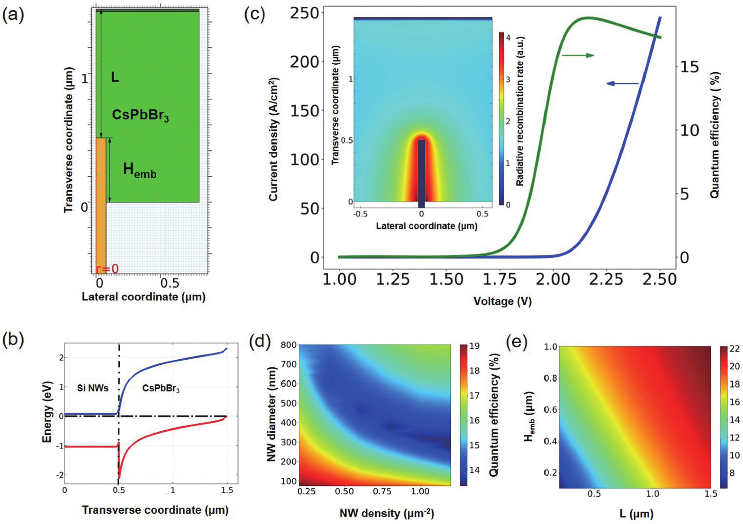
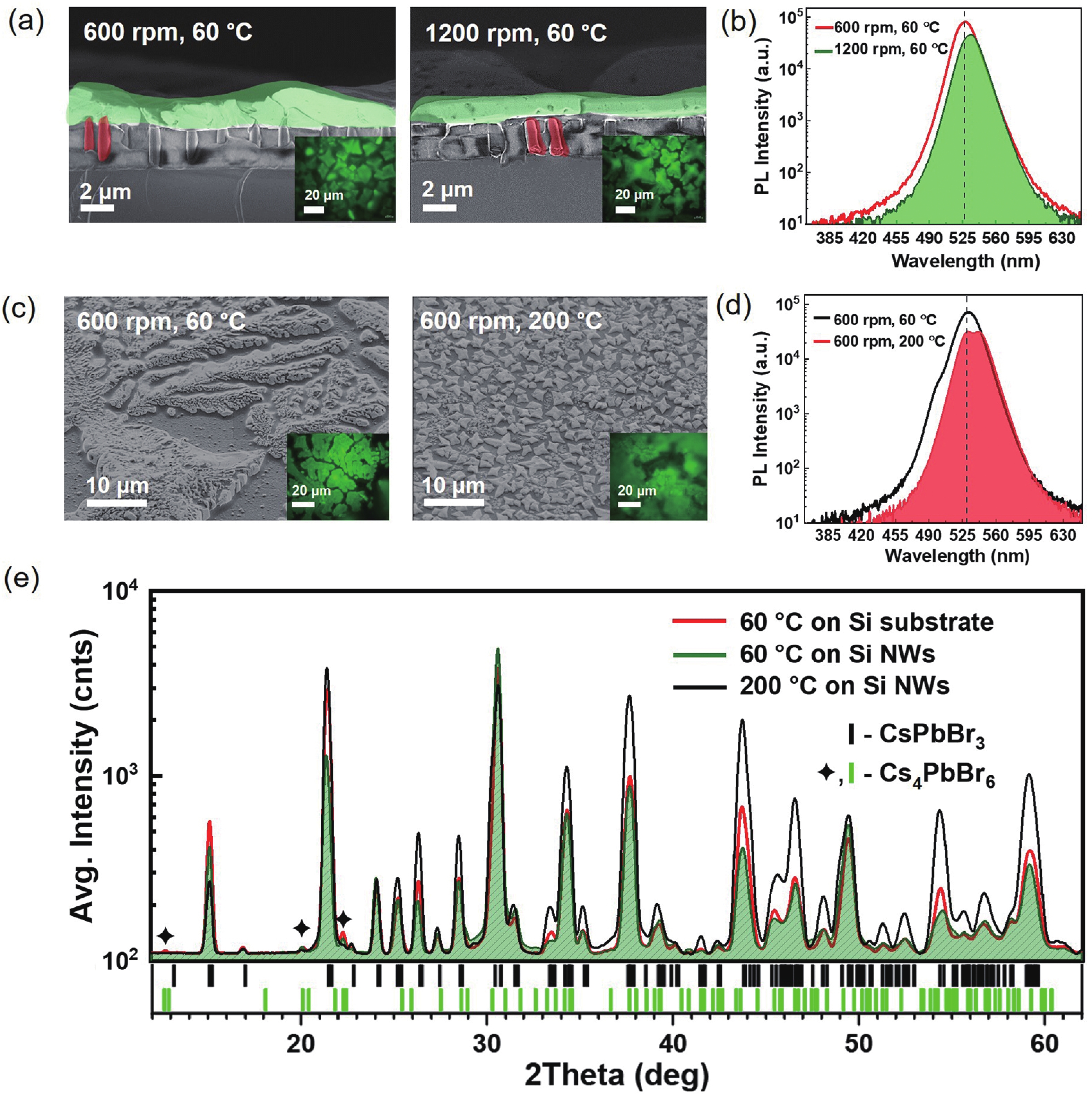
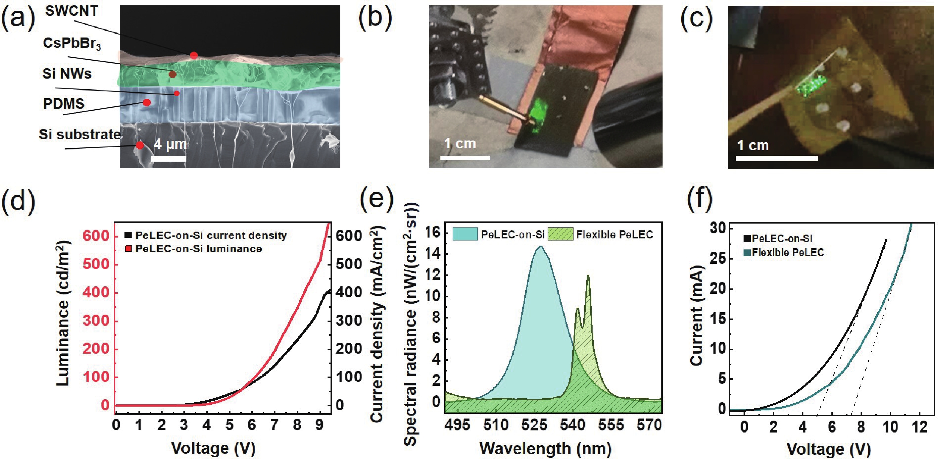
Baeva M, Gets D, Polushkin A, et al. ITO-free silicon-integrated perovskite electrochemical cell for light-emission and light-detection. Opto Electron Adv, 2023, 6(9), 220154 doi: 10.29026/oea.2023.220154 |
| [26] |
Prescher C, Prakapenka V B. DIOPTAS: A program for reduction of two-dimensional X-ray diffraction data and data exploration. High Press Res, 2015, 35(3), 223 doi: 10.1080/08957959.2015.1059835 |
| [27] |
Doebelin N, Kleeberg R. Profex: A graphical user interface for the Rietveld refinement program BGMN. J Appl Crystallogr, 2015, 48(Pt 5), 1573
|
| [28] |
Suturin S M, Fedorov V V, Korovin A M, et al. A look inside epitaxial cobalt-on-fluorite nanoparticles with three-dimensional reciprocal space mapping using GIXD, RHEED and GISAXS. J Appl Crystallogr, 2013, 46(4), 874 doi: 10.1107/S0021889813008777 |
| [29] |
Phung N, Mattoni A, Smith J A, et al. Photoprotection in metal halide perovskites by ionic defect formation. Joule, 2022, 6(9), 2152 doi: 10.1016/j.joule.2022.06.029 |
| [30] |
Liao K J, Li C B, Xie L S, et al. Hot-casting large-grain perovskite film for efficient solar cells: Film formation and device performance. Nanomicro Lett, 2020, 12(1), 156 doi: 10.1007/s40820-020-00494-2 |
| [31] |
Ummadisingu A, Meloni S, Mattoni A, et al. Crystal-size-induced band gap tuning in perovskite films. Angew Chem Int Ed, 2021, 60(39), 21368 doi: 10.1002/anie.202106394 |
| [32] |
Toso S, Baranov D, Giannini C, et al. Wide-angle X-ray diffraction evidence of structural coherence in CsPbBr 3 nanocrystal superlattices. ACS Mater Lett, 2019, 1(2), 272 doi: 10.1021/acsmaterialslett.9b00217 |
| [33] |
Veeramuthu L, Liang F C, Zhang Z X, et al. Improving the performance and stability of perovskite light-emitting diodes by a polymeric nanothick interlayer-assisted grain control process. ACS Omega, 2020, 5(15), 8972 doi: 10.1021/acsomega.0c00758 |
| [34] |
Warby J H, Wenger B, Ramadan A J, et al. Revealing factors influencing the operational stability of perovskite light-emitting diodes. ACS Nano, 2020, 14(7), 8855 doi: 10.1021/acsnano.0c03516 |
| [35] |
Morozov I, Gudovskikh A, Uvarov A, et al. The study of latex sphere lithography for high aspect ratio dry silicon etching. Phys Status Solidi A, 2020, 217(4), 1900535 doi: 10.1002/pssa.201900535 |
| [36] |
Vyacheslavova E A, Morozov I A, Kudryashov D A, et al. Formation of SiO 2 hard mask using dry etching and nanosphere lithography. J Phys: Conf Ser, 2020, 1697(1), 012188 doi: 10.1088/1742-6596/1697/1/012188 |
| [37] |
Neplokh V, Kochetkov F M, Deriabin K V, et al. Modified silicone rubber for fabrication and contacting of flexible suspended membranes of n-/p-GaP nanowires with a single-walled carbon nanotube transparent contact. J Mater Chem C, 2020, 8(11), 3764 doi: 10.1039/C9TC06239D |
| [38] |
Fedorov V V, Bolshakov A, Sergaeva O, et al. Gallium phosphide nanowires in a free-standing, flexible, and semitransparent membrane for large-scale infrared-to-visible light conversion. ACS Nano, 2020, 14(8), 10624 doi: 10.1021/acsnano.0c04872 |
| [39] |
Tian Y, Timmermans M Y, Partanen M, et al. Growth of single-walled carbon nanotubes with controlled diameters and lengths by an aerosol method. Carbon, 2011, 49(14), 4636 doi: 10.1016/j.carbon.2011.06.036 |
| [40] |
Khabushev E M, Kolodiazhnaia J V, Krasnikov D V, et al. Activation of catalyst particles for single-walled carbon nanotube synthesis. Chem Eng J, 2021, 413, 127475 doi: 10.1016/j.cej.2020.127475 |
| [41] |
Mkrtchyan A A, Gladush Y G, Galiakhmetova D, et al. Dry-transfer technique for polymer-free single-walled carbon nanotube saturable absorber on a side polished fiber. Opt Mater Express, 2019, 9(4), 1551 doi: 10.1364/OME.9.001551 |
| [42] |
Nasibulin A G, Kaskela A, Mustonen K, et al. Multifunctional free-standing single-walled carbon nanotube films. ACS Nano, 2011, 5(4), 3214 doi: 10.1021/nn200338r |
| [43] |
Chen D Z, Li X Y, Su A X, et al. Performance enhancement of perovskite solar cells via material quality improvement assisted by MAI/IPA solution post-treatment. Dalton Trans, 2019, 48(16), 5292 doi: 10.1039/C9DT00930B |
| [44] |
Jia P, Lu M, Sun S Q, et al. Recent advances in flexible perovskite light-emitting diodes. Adv Mater Inter, 2021, 8(17), 2100441 doi: 10.1002/admi.202100441 |
| [45] |
Calarco R, Stoica T, Brandt O, et al. Surface-induced effects in GaN nanowires. J Mater Res, 2011, 26(17), 2157 doi: 10.1557/jmr.2011.211 |
| [46] |
Kochetkov F M, Neplokh V, Fedorov V V, et al. Fabrication and electrical study of large area free-standing membrane with embedded GaP NWs for flexible devices. Nanotechnology, 2020, 31(46), 46LT01 doi: 10.1088/1361-6528/abae98 |
| [47] |
Stoumpos C C, Malliakas C D, Peters J A, et al. Crystal growth of the perovskite semiconductor CsPbBr 3: A new material for high-energy radiation detection. Cryst Growth Des, 2013, 13(7), 2722 doi: 10.1021/cg400645t |
| [48] |
De Bastiani M, Dursun I, Zhang Y H, et al. Inside perovskites: Quantum luminescence from bulk Cs 4PbBr 6 single crystals. Chem Mater, 2017, 29(17), 7108 doi: 10.1021/acs.chemmater.7b02415 |
| [49] |
Baeva M, Miroshnichenko A S, Kenesbay R, et al. Enhancing the CsPbBr 3 PeLEC properties via PDMS/PMHS double-layer polymer encapsulation and high relative humidity stress-aging. J Mater Chem C, 2023, 11(43), 15261 doi: 10.1039/D3TC01370G |
| [50] |
Ghaithan H M, Alahmed Z A, Qaid S M H, et al. Density functional study of cubic, tetragonal, and orthorhombic CsPbBr 3 perovskite. ACS Omega, 2020, 5(13), 7468 doi: 10.1021/acsomega.0c00197 |
| [51] |
Liu C, Chen H, Lin P, et al. Growth, characterization and photoelectrical properties of orthorhombic and cubic CsPbBr 3 single crystals. J Mater Sci Mater Electron, 2022, 33(32), 24895 doi: 10.1007/s10854-022-09199-1 |
| [52] |
Baitova V A, Knyazeva M A, Mukanov I A, et al. Evolution of the luminescence properties of single CsPbBr 3 perovskite nanocrystals during photodegradation. JETP Lett, 2023, 118(8), 560 doi: 10.1134/S002136402360283X |
| [53] |
Han Q J, Wu W Z, Liu W L, et al. The peak shift and evolution of upconversion luminescence from CsPbBr 3 nanocrystals under femtosecond laser excitation. RSC Adv, 2017, 7(57), 35757 doi: 10.1039/C7RA06211G |


 Viktoriia Mastalieva Victoriia Mastalieva was trained from 2020 to 2024 in the scientific speciality "Semiconductor Physics" at the Alferov Federal State Institution of the Russian Academy of Sciences in St. Petersburg (Renewable Energy Laboratory). Scientific supervisor is a specialist in flexible electronics Neplokh V. V. Now the focus of scientific interests includes nonlinear silicon photonics with high compatibility with CMOS technology. Nonlinear effects in silicon nanowires (NWs) are widely studied due to high sensitivity to structural changes, cheapness of fabrication and efficient tunability of photonic properties.
 Anastasiya Yakubova got her bachelor's degree in 2021 from the Saint Petersburg State Chemical and Pharmaceutical University and her master's degree in 2023 in Alferov University, Saint Petersburg. Now she is postgraduate student at Alferov University under supervision of Dr. Fedor Kochetkov. Her research focuses on flexible electronics, based on perovskite materials.
 DownLoad: