


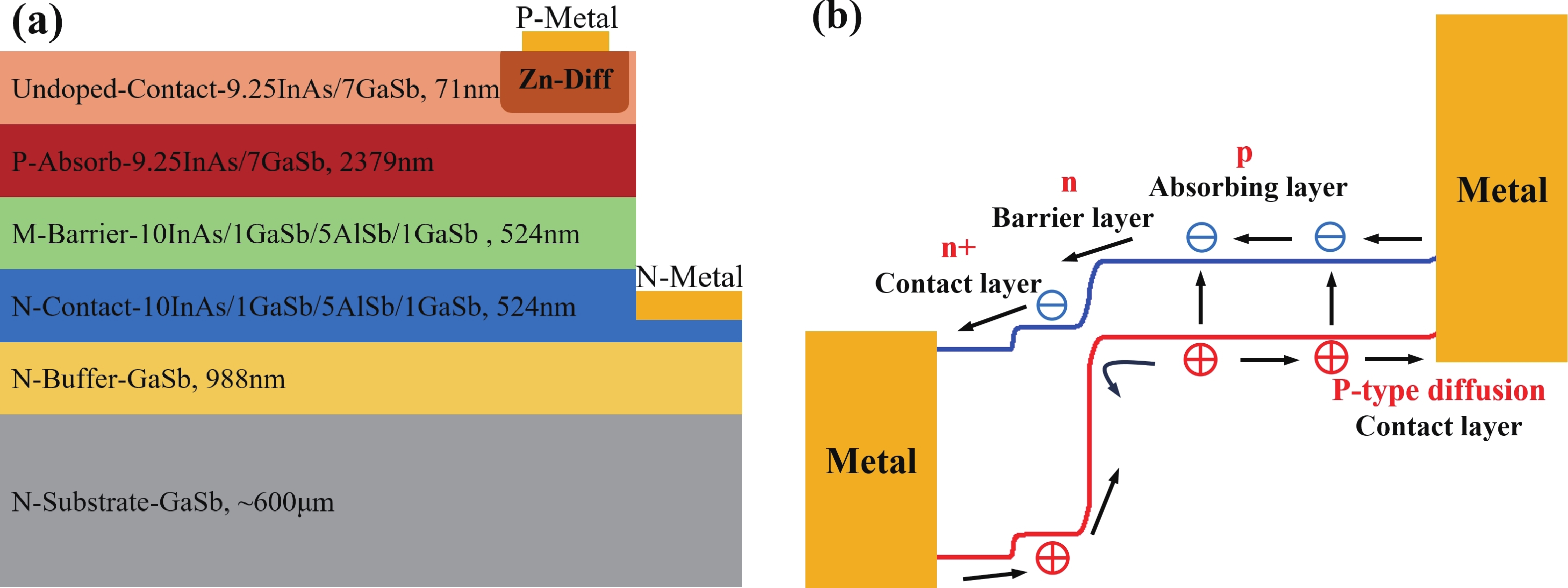
Fig. 1.
(Color online) The MWIR photodetector. (a) schematic diagram. (b) schematic band structure diagram.
ARTICLES
Shihao Zhang1, 2, Hongyue Hao1, 3, , Ye Zhang1, 3, Shuo Wang1, Xiangyu Zhang1, Ruoyu Xie1, 3, Lingze Yao1, Faran Chang1, Yifan shan1, 3, Haofeng Liu2, Guowei Wang1, 3, Donghai Wu1, 3, Dongwei Jiang1, 3, Yingqiang Xu1, 3, Zhichuan Niu1, 3 and Wenjing Dong2,
Corresponding author: Hongyue Hao, haohongyue@semi.ac.cn; Wenjing Dong, wenjingd@hubu.edu.cn
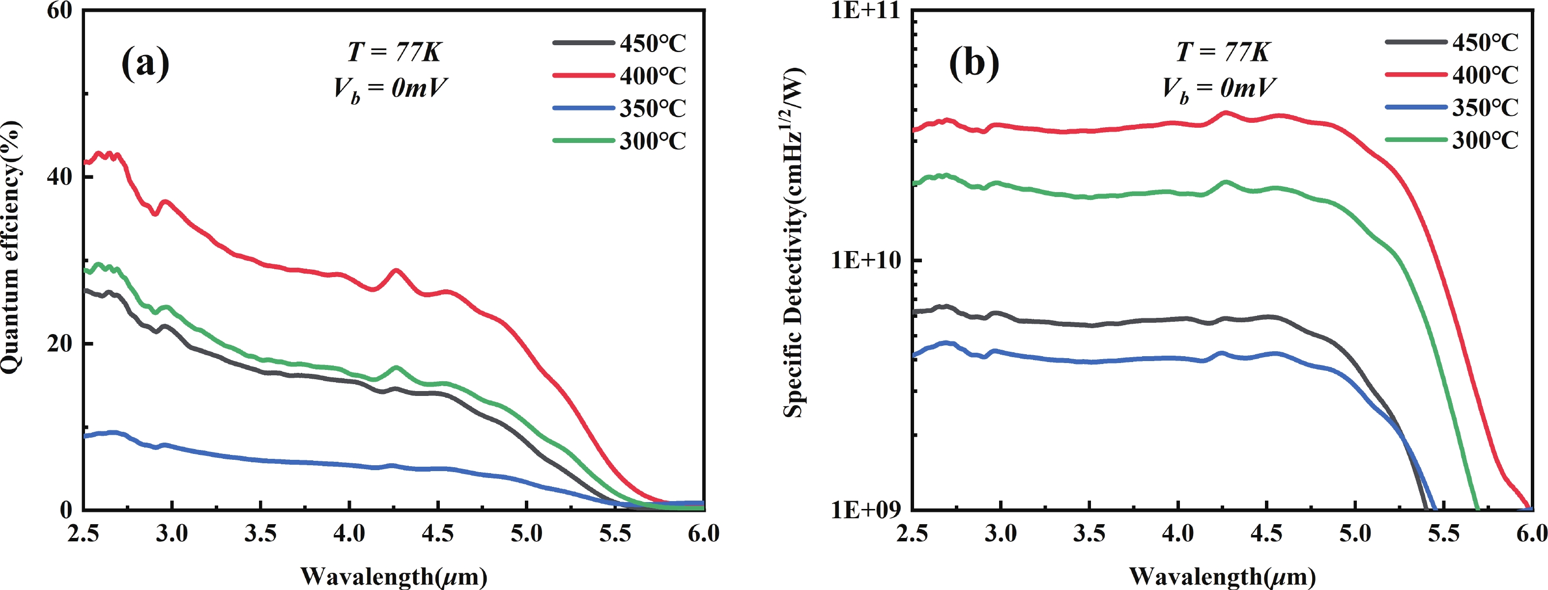
Abstract: In this paper, a planar junction mid-wavelength infrared (MWIR) photodetector based on an InAs/GaSb type-II superlattices (T2SLs) is reported. The Intrinsic-πMN superlattices was grown by the molecular beam epitaxy (MBE), followed with a ZnS layer grown by the chemical vapor deposition (CVD). The P-type contact layer was constructed by thermal diffusion in the undoped superlattices. The Zinc atom was successfully realised in to the superlattice and a PπMN T2SL structure was constructed. Furthermore, the effects of different diffusion temperatures on the dark current performance of the devices were researched. The 50% cut-off wavelength of the photodetector is 5.26 μm at 77K with 0V bias. The minimum dark current density is 8.67 × 10⁻⁵ A/cm2 and the maximum quantum efficiency of 42.5%, and the maximum detectivity reaches 3.90 × 1010 cm·Hz1/2/W at 77 K. The 640 × 512 focal plane arrays (FPA) based on the planner junction were fabricated afterwards. The FPA achieves a noise equivalent temperature difference (NETD) of 539 mK.
Key words: InAs /GaSb type-II superlattices, planar photodetector, mid-wavelength infrared, Zinc diffusion
| [1] |
Rogalski A. Progress in focal plane array technologies. Prog Quantum Electron, 2012, 36(2/3), 342
|
| [2] |
Dong C Y, An X, Wu Z C, et al. Multilayered PdTe2/thin Si heterostructures as self-powered flexible photodetectors with heart rate monitoring ability. J Semicond, 2023, 44(11), 112001 doi: 10.1088/1674-4926/44/11/112001
|
| [3] |
Rogalski A. HgCdTe infrared detector material: History, status and outlook. Rep Prog Phys, 2005, 68(10), 2267 doi: 10.1088/0034-4885/68/10/R01
|
| [4] |
Si J, Novel InSb-based infrared detector materials, Infrared and Laser engineering, 2022, 51(1), 20210811
|
| [5] |
Sai-Halasz G A, Tsu R, Esaki L. A new semiconductor superlattice. Appl Phys Lett, 1977, 30(12), 651 doi: 10.1063/1.89273
|
| [6] |
Smith D L, Mailhiot C. Proposal for strained type II superlattice infrared detectors. J Appl Phys, 1987, 62(6), 2545 doi: 10.1063/1.339468
|
| [7] |
Nguyen B M, Razeghi M, Nathan V, et al. Type-II M structure photodiodes: an alternative material design for mid-wave to long wavelength infrared regimes Quantum Sensing and Nanophotonic Devices IV, 2007
|
| [8] |
Grein C H, Young P M, Flatté M E, et al. Long wavelength InAs/InGaSb infrared detectors: Optimization of carrier lifetimes. 1995, 78(12), 7143
|
| [9] |
Rogalski A. Material considerations for third generation infrared photon detectors. Infrared Phys Technol, 2007, 50(2/3), 240
|
| [10] |
Delaunay P Y, Hood A, Nguyen B M, et al. Passivation of type-II InAs∕GaSb double heterostructure. 2007, 91(9), 0911, 12
|
| [11] |
Zhang Z, Yates J T Jr. Band bending in semiconductors: Chemical and physical consequences at surfaces and interfaces. Chem Rev, 2012, 112(10), 5520 doi: 10.1021/cr3000626
|
| [12] |
Plis E A. InAs/GaSb type-II superlattice detectors. Adv Electron, 2014, 2014, 246769
|
| [13] |
Marozas B T, Hughes W D, Du X, et al. Surface dark current mechanisms in III-V infrared photodetectors. Opt Mater Express, 2018, 8(6), 1419 doi: 10.1364/OME.8.001419
|
| [14] |
Salihoglu O, Muti A, Kutluer K, et al. Passivation of type II InAs/GaSb superlattice photodetectors with atomic layer deposited Al2O3. Infrared Technology and Applications XXXVIII. Baltimore, 2012, 83530Z
|
| [15] |
Hou X Y, Wen L J, He F Y, et al. Embedded high-quality ternary GaAs1–xSbx quantum dots in GaAs nanowires by molecular-beam epitaxy. J Semicond, 2024, 45(8), 082101 doi: 10.1088/1674-4926/24030038
|
| [16] |
Kinch M A. The rationale for ultra-small pitch IR systems. Infrared Technology and Applications XL. Baltimore, 2014
|
| [17] |
Cui Y Z, Hao H Y, Zhang S H, et al. High-performance GaSb planar PN junction detector. J Semicond, 2024, 45(9), 092403 doi: 10.1088/1674-4926/24040024
|
| [18] |
Musca C A, Antoszewski J, Dell J M, et al. Planar p-on-n HgCdTe heterojunction mid-wavelength infrared photodiodes formed using plasma-induced junction isolation. J Electron Mater, 2003, 32(7), 622 doi: 10.1007/s11664-003-0042-1
|
| [19] |
Iwamura Y, Watanabe N. InAs planar diode fabricated by Zn diffusion. Jpn J Appl Phys, 2000, 39(10R), 5740 doi: 10.1143/JJAP.39.5740
|
| [20] |
Pitts O J, Hisko M, Benyon W, et al. Optimization of MOCVD-diffused p-InP for planar avalanche photodiodes. J Cryst Growth, 2014, 393, 85 doi: 10.1016/j.jcrysgro.2013.09.053
|
| [21] |
Wang T T, Xiong M, Zhao Y C, et al. Planar mid-infrared InAsSb photodetector grown on GaAs substrates by MOCVD. Appl Phys Express, 2019, 12(12), 122009 doi: 10.7567/1882-0786/ab507c
|
| [22] |
Dehzangi A, Wu D H, McClintock R, et al. Demonstration of planar type-II superlattice-based photodetectors using silicon ion-implantation. Photonics, 2020, 7(3), 68 doi: 10.3390/photonics7030068
|
| [23] |
Wu D H, Dehzangi A, Li J K, et al. High performance Zn-diffused planar mid-wavelength infrared type-II InAs/InAs1−xSbx superlattice photodetector by MOCVD. 2020, 116(16), 1611, 08
|
| [24] |
Nguyen B M, Hoffman D, Delaunay P Y, et al. Dark current suppression in type II InAs/GaSb superlattice long wavelength infrared photodiodes with M-structure barrier. 2007, 91(16), 1635, 11
|
| [25] |
Simcock M N. Zinc diffusion in GaSb for thermophotovoltaic cell applications. Thermophotovoltaic Generation of Electricity: Sixth Conference on Thermophotovoltaic Generation of Electricity: TPV6, 2004, 303
|
| [26] |
Hao H Y, Wang G W, Xiang W, et al. Fabrication of type-II InAs/GaSb superlattice long-wavelength infrared focal plane arrays. Infrared Phys Technol, 2015, 72, 276 doi: 10.1016/j.infrared.2015.07.025
|
| [27] |
Mao J X, Zhuang J S. Calculation of Factor g in Measurement of Parameters of IRFPA Detectors. Infrared, 2008, 04, 8
|
| [28] |
Zhou X C, Li D S, Huang J L, et al. Mid-wavelength type II InAs/GaSb superlattice infrared focal plane arrays. Infrared Phys Technol, 2016, 78, 263 doi: 10.1016/j.infrared.2016.08.014
|
| [29] |
Rehm R, Walther M, Schmitz J, et al. InAs/GaSb superlattice focal plane arrays for high-resolution thermal imaging. Opto Electron Rev, 2006, 14(1), 19
|
| [30] |
Bogdanov S. Planar engineering for dark current suppression in type-II superlattice infrared photodiodes. Northwestern University, United States-Illinois, 2014, 172
|


Article views: 72 Times PDF downloads: 32 Times Cited by: 0 Times
Received: 12 December 2024 Revised: 15 May 2025 Online: Accepted Manuscript: 20 June 2025
| Citation: |
Shihao Zhang, Hongyue Hao, Ye Zhang, Shuo Wang, Xiangyu Zhang, Ruoyu Xie, Lingze Yao, Faran Chang, Yifan shan, Haofeng Liu, Guowei Wang, Donghai Wu, Dongwei Jiang, Yingqiang Xu, Zhichuan Niu, Wenjing Dong. Mid-wavelength infrared planar junction photodetector based on InAs/GaSb Type-II superlattices[J]. Journal of Semiconductors, 2025, In Press. doi: 10.1088/1674-4926/24120014
****
S H Zhang, H Y Hao, Y Zhang, S Wang, X Y Zhang, R Y Xie, L Z Yao, F R Chang, Y F shan, H F Liu, G W Wang, D H Wu, D W Jiang, Y Q Xu, Z C Niu, and W J Dong, Mid-wavelength infrared planar junction photodetector based on InAs/GaSb Type-II superlattices[J]. J. Semicond., 2025, accepted doi: 10.1088/1674-4926/24120014

|
 Shihao Zhang received a bachelor’s degree from Jingchu University of Technology in 2021. He is currently pursuing a master’s degree with the Hubei University. His present research interests include infrared detector of antimonide
 Hongyue Hao received her doctoral degree from the Institute of Semiconductors, Chinese Academy of Sciences in 2018. Following her PhD, she worked as a postdoctoral researcher in the Juelich Research Center in Germany. She is currently a Youth Researcher at the Institute of Semiconductors, Chinese Academy of Sciences. Her research focused on the Sb-based infrared detectors, especially including the broadband and multi-band detectors with meta-surface, low-cost, low noise and high sensitivity detectors
 Wenjing Dong received the Ph.D. degree in Microelectronics and Solid State Electronics from Shanghai Institute of Technical Physics, Chinese Academy of Sciences. She is currently an associate professor in Hubei University. She had been an visiting scholar in University of Maryland from 2019 to 2020. Her research interests include semiconductor materials and devices, solid state ionics and solid state electronics
| [1] |
Rogalski A. Progress in focal plane array technologies. Prog Quantum Electron, 2012, 36(2/3), 342
|
| [2] |
Dong C Y, An X, Wu Z C, et al. Multilayered PdTe2/thin Si heterostructures as self-powered flexible photodetectors with heart rate monitoring ability. J Semicond, 2023, 44(11), 112001 doi: 10.1088/1674-4926/44/11/112001
|
| [3] |
Rogalski A. HgCdTe infrared detector material: History, status and outlook. Rep Prog Phys, 2005, 68(10), 2267 doi: 10.1088/0034-4885/68/10/R01
|
| [4] |
Si J, Novel InSb-based infrared detector materials, Infrared and Laser engineering, 2022, 51(1), 20210811
|
| [5] |
Sai-Halasz G A, Tsu R, Esaki L. A new semiconductor superlattice. Appl Phys Lett, 1977, 30(12), 651 doi: 10.1063/1.89273
|
| [6] |
Smith D L, Mailhiot C. Proposal for strained type II superlattice infrared detectors. J Appl Phys, 1987, 62(6), 2545 doi: 10.1063/1.339468
|
| [7] |
Nguyen B M, Razeghi M, Nathan V, et al. Type-II M structure photodiodes: an alternative material design for mid-wave to long wavelength infrared regimes Quantum Sensing and Nanophotonic Devices IV, 2007
|
| [8] |
Grein C H, Young P M, Flatté M E, et al. Long wavelength InAs/InGaSb infrared detectors: Optimization of carrier lifetimes. 1995, 78(12), 7143
|
| [9] |
Rogalski A. Material considerations for third generation infrared photon detectors. Infrared Phys Technol, 2007, 50(2/3), 240
|
| [10] |
Delaunay P Y, Hood A, Nguyen B M, et al. Passivation of type-II InAs∕GaSb double heterostructure. 2007, 91(9), 0911, 12
|
| [11] |
Zhang Z, Yates J T Jr. Band bending in semiconductors: Chemical and physical consequences at surfaces and interfaces. Chem Rev, 2012, 112(10), 5520 doi: 10.1021/cr3000626
|
| [12] |
Plis E A. InAs/GaSb type-II superlattice detectors. Adv Electron, 2014, 2014, 246769
|
| [13] |
Marozas B T, Hughes W D, Du X, et al. Surface dark current mechanisms in III-V infrared photodetectors. Opt Mater Express, 2018, 8(6), 1419 doi: 10.1364/OME.8.001419
|
| [14] |
Salihoglu O, Muti A, Kutluer K, et al. Passivation of type II InAs/GaSb superlattice photodetectors with atomic layer deposited Al2O3. Infrared Technology and Applications XXXVIII. Baltimore, 2012, 83530Z
|
| [15] |
Hou X Y, Wen L J, He F Y, et al. Embedded high-quality ternary GaAs1–xSbx quantum dots in GaAs nanowires by molecular-beam epitaxy. J Semicond, 2024, 45(8), 082101 doi: 10.1088/1674-4926/24030038
|
| [16] |
Kinch M A. The rationale for ultra-small pitch IR systems. Infrared Technology and Applications XL. Baltimore, 2014
|
| [17] |
Cui Y Z, Hao H Y, Zhang S H, et al. High-performance GaSb planar PN junction detector. J Semicond, 2024, 45(9), 092403 doi: 10.1088/1674-4926/24040024
|
| [18] |
Musca C A, Antoszewski J, Dell J M, et al. Planar p-on-n HgCdTe heterojunction mid-wavelength infrared photodiodes formed using plasma-induced junction isolation. J Electron Mater, 2003, 32(7), 622 doi: 10.1007/s11664-003-0042-1
|
| [19] |
Iwamura Y, Watanabe N. InAs planar diode fabricated by Zn diffusion. Jpn J Appl Phys, 2000, 39(10R), 5740 doi: 10.1143/JJAP.39.5740
|
| [20] |
Pitts O J, Hisko M, Benyon W, et al. Optimization of MOCVD-diffused p-InP for planar avalanche photodiodes. J Cryst Growth, 2014, 393, 85 doi: 10.1016/j.jcrysgro.2013.09.053
|
| [21] |
Wang T T, Xiong M, Zhao Y C, et al. Planar mid-infrared InAsSb photodetector grown on GaAs substrates by MOCVD. Appl Phys Express, 2019, 12(12), 122009 doi: 10.7567/1882-0786/ab507c
|
| [22] |
Dehzangi A, Wu D H, McClintock R, et al. Demonstration of planar type-II superlattice-based photodetectors using silicon ion-implantation. Photonics, 2020, 7(3), 68 doi: 10.3390/photonics7030068
|
| [23] |
Wu D H, Dehzangi A, Li J K, et al. High performance Zn-diffused planar mid-wavelength infrared type-II InAs/InAs1−xSbx superlattice photodetector by MOCVD. 2020, 116(16), 1611, 08
|
| [24] |
Nguyen B M, Hoffman D, Delaunay P Y, et al. Dark current suppression in type II InAs/GaSb superlattice long wavelength infrared photodiodes with M-structure barrier. 2007, 91(16), 1635, 11
|
| [25] |
Simcock M N. Zinc diffusion in GaSb for thermophotovoltaic cell applications. Thermophotovoltaic Generation of Electricity: Sixth Conference on Thermophotovoltaic Generation of Electricity: TPV6, 2004, 303
|
| [26] |
Hao H Y, Wang G W, Xiang W, et al. Fabrication of type-II InAs/GaSb superlattice long-wavelength infrared focal plane arrays. Infrared Phys Technol, 2015, 72, 276 doi: 10.1016/j.infrared.2015.07.025
|
| [27] |
Mao J X, Zhuang J S. Calculation of Factor g in Measurement of Parameters of IRFPA Detectors. Infrared, 2008, 04, 8
|
| [28] |
Zhou X C, Li D S, Huang J L, et al. Mid-wavelength type II InAs/GaSb superlattice infrared focal plane arrays. Infrared Phys Technol, 2016, 78, 263 doi: 10.1016/j.infrared.2016.08.014
|
| [29] |
Rehm R, Walther M, Schmitz J, et al. InAs/GaSb superlattice focal plane arrays for high-resolution thermal imaging. Opto Electron Rev, 2006, 14(1), 19
|
| [30] |
Bogdanov S. Planar engineering for dark current suppression in type-II superlattice infrared photodiodes. Northwestern University, United States-Illinois, 2014, 172
|

 WeChat ID
Journal of Semiconductors © 2017 All Rights Reserved 京ICP备05085259号-2

 DownLoad:

