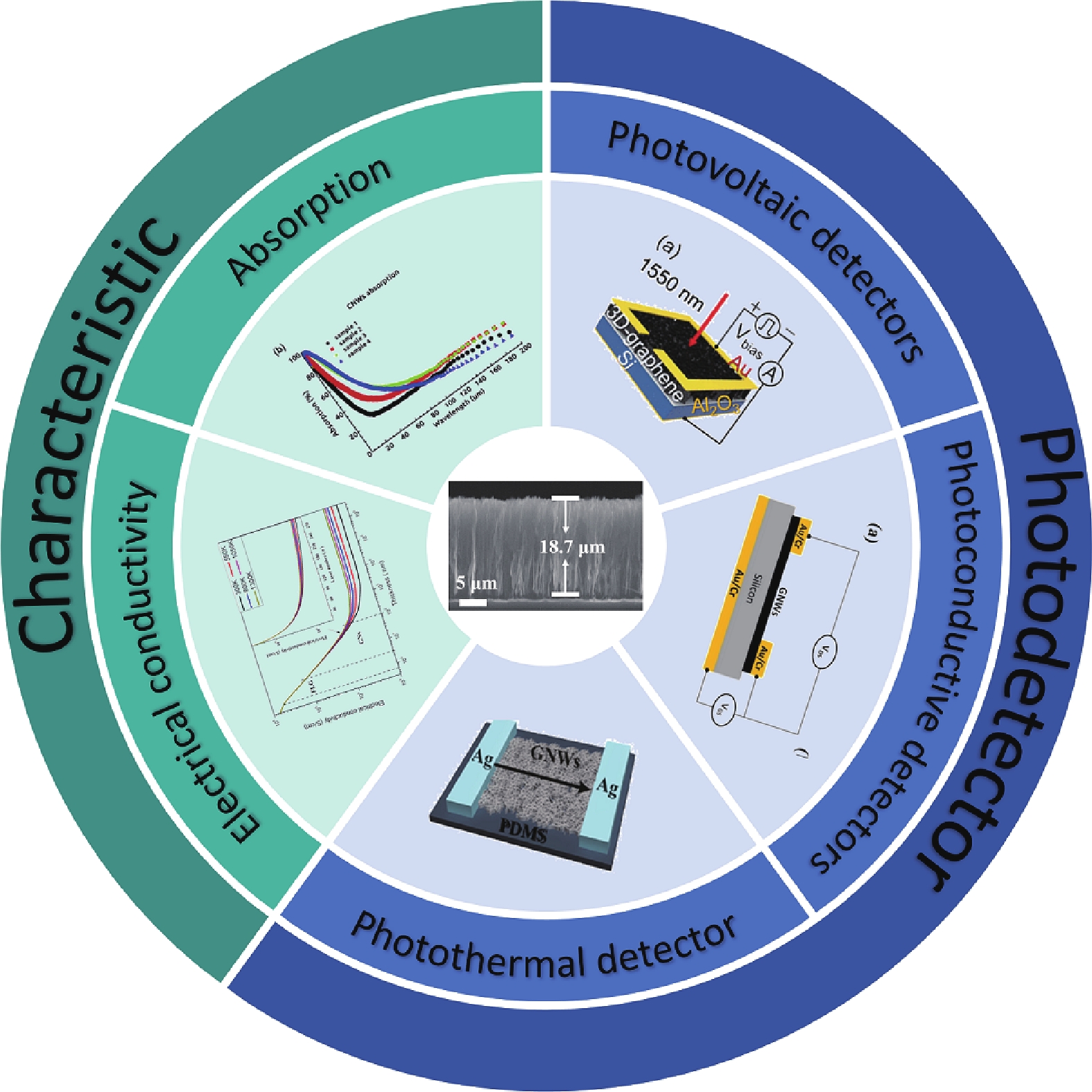
Fig. 1.
(Color online) Properties and applications of 3D-graphene.
REVIEWS
Bingkun Wang1, Jinqiu Zhang1, Huijuan Wu1, Fanghao Zhu1, Shanshui Lian1, Genqiang Cao1, Hui Ma1, Xurui Hu1, , Li Zheng2, and Gang Wang1, 2,
Corresponding author: Xurui Hu, huxurui@nbu.edu.cn; Li Zheng, zhengli@mail.sim.ac.cn; Gang Wang, gangwang@nbu.edu.cn
Abstract: Graphene has garnered significant attention in photodetection due to its exceptional optical, electrical, mechanical, and thermal properties. However, the practical application of two-dimensional (2D) graphene in optoelectronic fields is limited by its weak light absorption (only 2.3%) and zero bandgap characteristics. Increasing light absorption is a critical scientific challenge for developing high-performance graphene-based photodetectors. Three-dimensional (3D) graphene comprises vertically grown stacked 2D-graphene layers and features a distinctive porous structure. Unlike 2D-graphene, 3D-graphene offers a larger specific surface area, improved electrochemical activity, and high chemical stability, making it a promising material for optoelectronic detection. Importantly, 3D-graphene has an optical microcavity structure that enhances light absorption through interaction with incoming light. This paper systematically reviews and analyzes the current research status and challenges of 3D-graphene-based photodetectors, aiming to explore feasible development paths for these devices and promote their industrial application.
Keywords: 3D-graphene, growth techniques, heterojunctions, photodetectors
| [1] |
Liang S, Wang F F, Ma Z, et al. Asymmetric light excitation for photodetectors based on nanoscale semiconductors. ACS Nano, 2017, 11(1), 549 doi: 10.1021/acsnano.6b06598
|
| [2] |
Hu X, Wu J H, Wu M Z, et al. Recent developments of infrared photodetectors with low-dimensional inorganic nanostructures. Nano Res, 2022, 15(2), 805 doi: 10.1007/s12274-021-3634-2
|
| [3] |
Pan Q, Su M, Zhang Z Y, et al. Omnidirectional photodetectors based on spatial resonance asymmetric facade via a 3D self-standing strategy. Advanced Materials, 2020, 32, 1907280 doi: 10.1002/adma.201907280
|
| [4] |
Chen M, Wang Y X, Zhao Z R. Monolithic metamaterial-integrated graphene terahertz photodetector with wavelength and polarization selectivity. ACS Nano, 2022, 16(10), 17263 doi: 10.1021/acsnano.2c07968
|
| [5] |
Gayduchenko I, Xu S G, Alymov G, et al. Tunnel field-effect transistors for sensitive terahertz detection. Nat Commun, 2021, 12(1), 543 doi: 10.1038/s41467-020-20721-z
|
| [6] |
He X W, Wang X, Nanot S, et al. Photothermoelectric p-n junction photodetector with intrinsic broadband polarimetry based on macroscopic carbon nanotube films. ACS Nano, 2013, 7(8), 7271 doi: 10.1021/nn402679u
|
| [7] |
Li L L, Xu H, Li Z X, et al. CMOS-compatible tellurium/silicon ultra-fast near-infrared photodetector. Small, 2023, 19(42), 2303114 doi: 10.1002/smll.202303114
|
| [8] |
Wei B B, Zou B Q, Liu J X, et al. Polarization-sensitive photodetector based on quasi-1D (TaSe4)2I nanowire response to 10.6 µm. Adv Funct Materials, 2024, 34(30), 2315194 doi: 10.1002/adfm.202315194
|
| [9] |
He Z Y, Du X Y, Yu X, et al. Reverse-distribution phase featured gradient heterojunction: A universal strategy to realize high-performance near-infrared organic photodetectors for real-time arterial monitoring. Nano Energy, 2023, 114, 108673 doi: 10.1016/j.nanoen.2023.108673
|
| [10] |
Zhou Y C, Yang J, Bai L, et al. Flexible phase change hydrogels for mid-/low-temperature infrared stealth. Chemical Engineering Journal, 2022, 446, 137463 doi: 10.1016/j.cej.2022.137463
|
| [11] |
Zhou Z Q, Shen T, Wang P, et al. Low symmetric sub-wavelength array enhanced lensless polarization-sensitivity photodetector of germanium selenium. Sci Bull, 2023, 68(2), 173 doi: 10.1016/j.scib.2023.01.013
|
| [12] |
Wang F, Zhang T, Xie R, et al. Next-generation photodetectors beyond van der waals junctions. Adv Mater, 2024, 36(3), e2301197 doi: 10.1002/adma.202301197
|
| [13] |
Gao L F, Zhao Y M, Chang X H, et al. Emerging applications of MXenes for photodetection: Recent advances and future challenges. Mater Today, 2022, 61, 169 doi: 10.1016/j.mattod.2022.10.022
|
| [14] |
Pan X Y, Ding L M. Application of metal halide perovskite photodetectors. J Semicond, 2022, 43(2), 020203 doi: 10.1088/1674-4926/43/2/020203
|
| [15] |
Novoselov K S, Geim A K, Morozov S V, et al. Electric field effect in atomically thin carbon films. Science, 2004, 306(5696), 666 doi: 10.1126/science.1102896
|
| [16] |
Zhao C C, Liu Y Y, Wang D B, et al. High-performance self-driven broadband photoelectrochemical photodetector based on reduced graphene oxide/Bi2Te3 heterojunction. Nano Mater Sci, 2024, 6(6), 741 doi: 10.1016/j.nanoms.2023.12.008
|
| [17] |
Echtermeyer T J, Britnell L, Jasnos P K, et al. Strong plasmonic enhancement of photovoltage in graphene. Nat Commun, 2011, 2, 458 doi: 10.1038/ncomms1464
|
| [18] |
Chang H X, Wu H K. Graphene-based nanomaterials: Synthesis, properties, and optical and optoelectronic applications. Adv Funct Materials, 2013, 23(16), 1984 doi: 10.1002/adfm.201202460
|
| [19] |
Sinitskii A. A recipe for nanoporous graphene. Science, 2018, 360(6385), 154 doi: 10.1126/science.aat5117
|
| [20] |
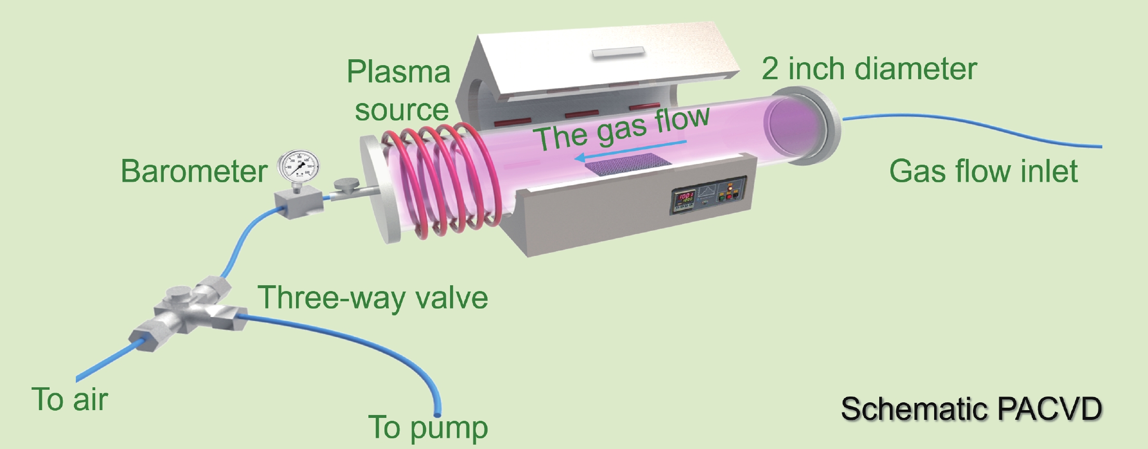
Li P L, Wei W Y, Zhang M, et al. Wafer-scale growth of single-crystal graphene on vicinal Ge(001) substrate. Nano Today, 2020, 34, 100908 doi: 10.1016/j.nantod.2020.100908
|
| [21] |
Zhang X, Jing Q, Ao S, et al. Ultrasensitive field-effect biosensors enabled by the unique electronic properties of graphene. Small, 2020, 16(15), e1902820 doi: 10.1002/smll.201902820
|
| [22] |
Koepfli S M, Baumann M, Koyaz Y, et al. Metamaterial graphene photodetector with bandwidth exceeding 500 gigahertz. Science, 2023, 380(6650), 1169 doi: 10.1126/science.adg8017
|
| [23] |
Du S C, Lu W, Ali A, et al. A broadband fluorographene photodetector. Adv Mater, 2017, 29(22), 1700463 doi: 10.1002/adma.201700463
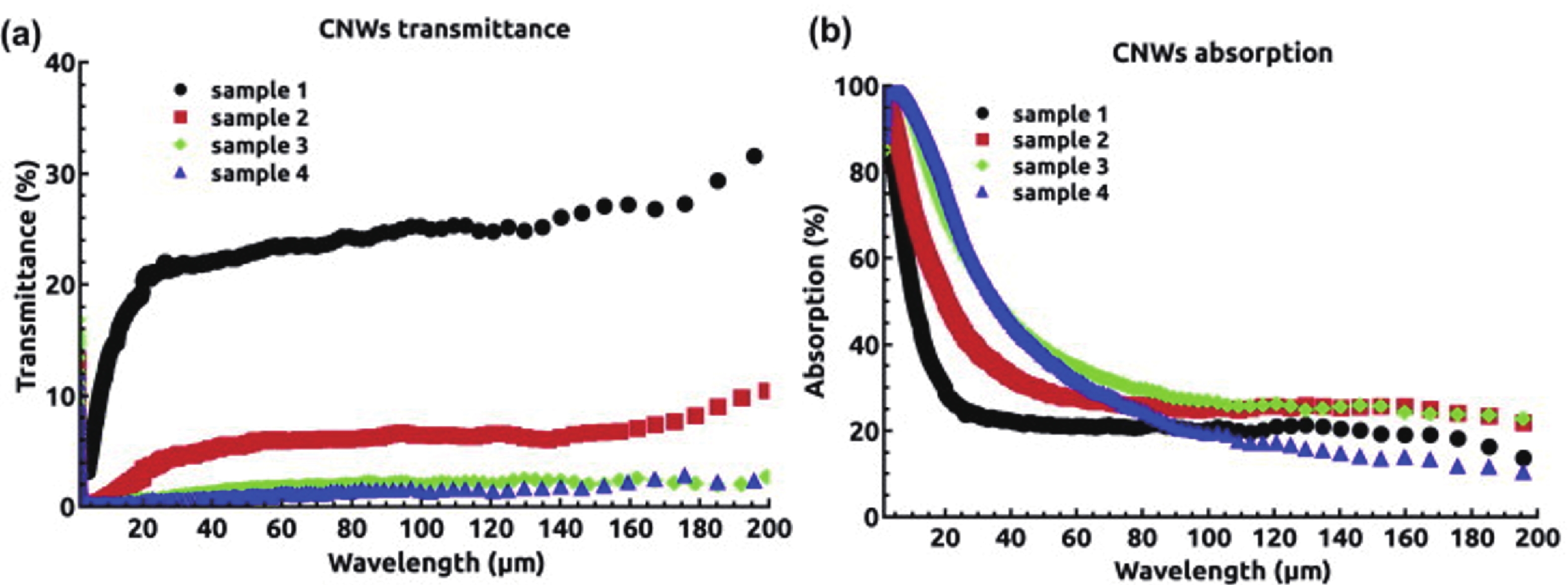
|
| [24] |
Biccari F, Gabelloni F, Burzi E, et al. Graphene-based electron transport layers in perovskite solar cells: A step-up for an efficient carrier collection. Adv Energy Mater, 2017, 7(22), 1701349 doi: 10.1002/aenm.201701349
|
| [25] |
Agresti A, Pescetelli S, Cinà L, et al. Efficiency and stability enhancement in perovskite solar cells by inserting lithium-neutralized graphene oxide as electron transporting layer. Adv Funct Materials, 2016, 26(16), 2686 doi: 10.1002/adfm.201504949
|
| [26] |
Du S C, Xie H, Yin J X, et al. Giant hot electron thermalization via stacking of graphene layers. Carbon, 2023, 203, 835 doi: 10.1016/j.carbon.2022.12.017
|
| [27] |
Sassi U, Parret R, Nanot S, et al. Graphene-based mid-infrared room-temperature pyroelectric bolometers with ultrahigh temperature coefficient of resistance. Nat Commun, 2017, 8, 14311 doi: 10.1038/ncomms14311
|
| [28] |
Nair R R, Blake P, Grigorenko A N, et al. Fine structure constant defines visual transparency of graphene. Science, 2008, 320(5881), 1308 doi: 10.1126/science.1156965
|
| [29] |
Elias D C, Nair R R, Mohiuddin T G, et al. Control of graphene’s properties by reversible hydrogenation: Evidence for graphane. Science, 2009, 323(5914), 610 doi: 10.1126/science.1167130
|
| [30] |
Castro E V, Novoselov K S, Morozov S V, et al. Biased bilayer graphene: Semiconductor with a gap tunable by the electric field effect. Phys Rev Lett, 2007, 99(21), 216802 doi: 10.1103/PhysRevLett.99.216802
|
| [31] |
Yin J B, Wang H, Peng H, et al. Selectively enhanced photocurrent generation in twisted bilayer graphene with van Hove singularity. Nat Commun, 2016, 7, 10699 doi: 10.1038/ncomms10699
|
| [32] |
Peng Y Y, Zhao W W, Ni F, et al. Forest-like laser-induced graphene film with ultrahigh solar energy utilization efficiency. ACS Nano, 2021, 15(12), 19490 doi: 10.1021/acsnano.1c06277
|
| [33] |
Zhang Q Q, You X, Tian L, et al. Fabrication and efficient electromagnetic waves attenuation of three-dimensional porous reduced graphene oxide/boron nitride/silicon carbide hierarchical structures. J Mater Sci Technol, 2023, 155, 192 doi: 10.1016/j.jmst.2022.12.056
|
| [34] |
Deng T, Zhang Z H, Liu Y X, et al. Three-dimensional graphene field-effect transistors as high-performance photodetectors. Nano Lett, 2019, 19(3), 1494 doi: 10.1021/acs.nanolett.8b04099
|
| [35] |
Olatomiwa A L, Adam T, Gopinath S C B, et al. Graphene synthesis, fabrication, characterization based on bottom-up and top-down approaches: An overview. J Semicond, 2022, 43(6), 061101 doi: 10.1088/1674-4926/43/6/061101
|
| [36] |
Shivananju B N, Yu W, Liu Y, et al. The roadmap of graphene-based optical biochemical sensors. Adv Funct Materials, 2016, 27, 1603918 doi: 10.1002/adfm.201603918
|
| [37] |
Cheng H H, Zhao F, Xue J L, et al. One single graphene oxide film for responsive actuation. ACS Nano, 2016, 10(10), 9529 doi: 10.1021/acsnano.6b04769
|
| [38] |
Fratzl P, Barth F G. Biomaterial systems for mechanosensing and actuation. Nature, 2009, 462(7272), 442 doi: 10.1038/nature08603
|
| [39] |
Ma T, Gao H L, Cong H P, et al. A bioinspired interface design for improving the strength and electrical conductivity of graphene-based fibers. Adv Mater, 2018, 30(15), 1706435 doi: 10.1002/adma.201706435
|
| [40] |
Stankovich S, Dikin D A, Dommett G H B, et al. Graphene-based composite materials. Nature, 2006, 442(7100), 282 doi: 10.1038/nature04969
|
| [41] |
Sadasivuni K K, Ponnamma D, Thomas S, et al. Evolution from graphite to graphene elastomer composites. Prog Polym Sci, 2014, 39(4), 749 doi: 10.1016/j.progpolymsci.2013.08.003
|
| [42] |
Li G Z, Huang B, Pan Z F, et al. Advances in three-dimensional graphene-based materials: Configurations, preparation and application in secondary metal (Li, Na, K, Mg, Al)-ion batteries. Energy Environ Sci, 2019, 12(7), 2030 doi: 10.1039/C8EE03014F
|
| [43] |
D’Apuzzo F, Piacenti A R, Giorgianni F, et al. Terahertz and mid-infrared plasmons in three-dimensional nanoporous graphene. Nat Commun, 2017, 8, 14885 doi: 10.1038/ncomms14885
|
| [44] |
Shi J L, Wang H F, Zhu X L, et al. The nanostructure preservation of 3D porous graphene: New insights into the graphitization and surface chemistry of non-stacked double-layer templated graphene after high-temperature treatment. Carbon, 2016, 103, 36 doi: 10.1016/j.carbon.2016.03.002
|
| [45] |
Ma Y F, Chen Y S. Three-dimensional graphene networks: Synthesis, properties and applications. Natl Sci Rev, 2015, 2(1), 40 doi: 10.1093/nsr/nwu072
|
| [46] |
Ando Y, Zhao X, Ohkohchi M. Production of petal-like graphite sheets by hydrogen arc discharge. Carbon, 1997, 35(1), 153 doi: 10.1016/S0008-6223(96)00139-X
|
| [47] |
Wu Y, Qiao P, Chong T, et al. Carbon nanowalls grown by microwave plasma enhanced chemical vapor deposition. Adv Mater, 2002, 14(1), 64 doi: 10.1002/1521-4095(20020104)14:1<64::AID-ADMA64>3.0.CO;2-G
|
| [48] |
Zhao J, Shaygan M, Eckert J, et al. A growth mechanism for free-standing vertical graphene. Nano Lett, 2014, 14(6), 3064 doi: 10.1021/nl501039c
|
| [49] |
Akhavan O, Ghaderi E, Rahighi R. Toward single-DNA electrochemical biosensing by graphene nanowalls. ACS Nano, 2012, 6(4), 2904 doi: 10.1021/nn300261t
|
| [50] |
Zhang L X, Sun Z, Qi J L, et al. Understanding the growth mechanism of vertically aligned graphene and control of its wettability. Carbon, 2016, 103, 339 doi: 10.1016/j.carbon.2016.03.029
|
| [51] |
Hojati-Talemi P, Simon G P. Field emission study of graphene nanowalls prepared by microwave-plasma method. Carbon, 2011, 49(8), 2875 doi: 10.1016/j.carbon.2011.03.004
|
| [52] |
Tang B, Wang S L, Zhang J, et al. Three-dimensional graphene monolith-based composite: Superiority in properties and applications. Int Mater Rev, 2018, 63(3), 204 doi: 10.1080/09506608.2017.1344377
|
| [53] |
Jin S X, Feng Y Y, Jia J C, et al. Three-dimensional N-doped carbon nanotube/graphene composite aerogel anode to develop high-power microbial fuel cell. Energy Environ Mater, 2023, 6(3), e12373 doi: 10.1002/eem2.12373
|
| [54] |
Yang Y, Liu T Y, Liao Q, et al. A three-dimensional nitrogen-doped graphene aerogel-activated carbon composite catalyst that enables low-cost microfluidic microbial fuel cells with superior performance. J Mater Chem A, 2016, 4(41), 15913 doi: 10.1039/C6TA05002F
|
| [55] |
Zhang Z Y, Li W Y, Yuen M F, et al. Hierarchical composite structure of few-layers MoS2 nanosheets supported by vertical graphene on carbon cloth for high-performance hydrogen evolution reaction. Nano Energy, 2015, 18, 196 doi: 10.1016/j.nanoen.2015.10.014
|
| [56] |
Ye S B, Feng J C. Towards three-dimensional, multi-functional graphene-based nanocomposite aerogels by hydrophobicity-driven absorption. J Mater Chem A, 2014, 2(27), 10365 doi: 10.1039/c4ta01392a
|
| [57] |
Zheng X L, Xiong X, Yang J W, et al. A strong and compressible three dimensional graphene/polyurushiol composite for efficient water cleanup. Chem Eng J, 2018, 333, 153 doi: 10.1016/j.cej.2017.09.146
|
| [58] |
Sun S M, Wang S, Li S D, et al. Asymmetric supercapacitors based on a NiCo2O4/three dimensional graphene composite and three dimensional graphene with high energy density. J Mater Chem A, 2016, 4(47), 18646 doi: 10.1039/C6TA07746C
|
| [59] |
Zhao X Y, Li X L, Zhang S L, et al. A three-dimensional sponge of graphene nanoribbons crosslinked by Fe3O4 nanoparticles for Li+ storage. J Mater Chem A, 2017, 5(45), 23592 doi: 10.1039/C7TA07874A
|
| [60] |
He M L, Wu L Y, Yu A L, et al. Surface functionalization of vertical graphene significantly enhances the energy storage capability for symmetric supercapacitors. Carbon, 2024, 216, 118511 doi: 10.1016/j.carbon.2023.118511
|
| [61] |
Ma J H, Wang P, Dong L, et al. Highly conductive, mechanically strong graphene monolith assembled by three-dimensional printing of large graphene oxide. J Colloid Interface Sci, 2019, 534, 12 doi: 10.1016/j.jcis.2018.08.096
|
| [62] |
Mo Y C, Yang K C, Lin J S, et al. CoSe2 anchored vertical graphene/macroporous carbon nanofibers used as multifunctional interlayers for high-performance lithium–sulfur batteries. J Mater Chem A, 2023, 11(12), 6349 doi: 10.1039/D2TA10020G
|
| [63] |
Wang S, Wang X, Sun C L, et al. Room-temperature fast assembly of 3D macroscopically porous graphene frameworks for binder-free compact supercapacitors with high gravimetric and volumetric capacitances. J Energy Chem, 2021, 61, 23 doi: 10.1016/j.jechem.2021.01.019
|
| [64] |
Rajackaitė E, Peckus D, Gudaitis R, et al. The evolution of properties with deposition time of vertical graphene nanosheets produced by microwave plasma-enhanced chemical vapor deposition. Surf Interfaces, 2021, 27, 101529 doi: 10.1016/j.surfin.2021.101529
|
| [65] |
Hiramatsu M, Shiji K, Amano H, et al. Fabrication of vertically aligned carbon nanowalls using capacitively coupled plasma-enhanced chemical vapor deposition assisted by hydrogen radical injection. Appl Phy Lett, 2004, 84(23), 4708 doi: 10.1063/1.1762702
|
| [66] |
Ma Y, Chaitoglou S, Farid G, et al. Supercapacitive performance of electrodes based on defective ZnO nanorods anchored on graphene nanowalls. Chem Eng J, 2024, 488, 151135 doi: 10.1016/j.cej.2024.151135
|
| [67] |
Qi Y, Deng B, Guo X, et al. Switching vertical to horizontal graphene growth using faraday cage-assisted PECVD approach for high-performance transparent heating device. Adv Mater, 2018, 30, 1704839 doi: 10.1002/adma.201704839
|
| [68] |
Li J R, Liu Z D, Guo Q L, et al. Controllable growth of vertically oriented graphene for high sensitivity gas detection. J Mater Chem C, 2019, 7(20), 5995 doi: 10.1039/C9TC01246J
|
| [69] |
Li J R, Guo Q L, Zhang N, et al. Direct integration of polycrystalline graphene on silicon as a photodetector via plasma-assisted chemical vapor deposition. J Mater Chem C, 2018, 6(36), 9682 doi: 10.1039/C8TC02646G
|
| [70] |
Xu S C, Wang S S, Chen Z, et al. Electric-field-assisted growth of vertical graphene arrays and the application in thermal interface materials. Adv Funct Materials, 2020, 30(34), 2003302 doi: 10.1002/adfm.202003302
|
| [71] |
Davami K, Shaygan M, Kheirabi N, et al. Synthesis and characterization of carbon nanowalls on different substrates by radio frequency plasma enhanced chemical vapor deposition. Carbon, 2014, 72, 372 doi: 10.1016/j.carbon.2014.02.025
|
| [72] |
He Z Y, Zhang G L, Zhang S, et al. Resonant nanocavity-enhanced graphene photodetectors on reflecting silicon-on-insulator wafers. Appl Phys Lett, 2021, 119(23), 232104 doi: 10.1063/5.0074703
|
| [73] |
Simionescu O G, Avram A, Adiaconiţă B, et al. Field-effect transistors based on single-layer graphene and graphene-derived materials. Micromachines, 2023, 14(6), 1096 doi: 10.3390/mi14061096
|
| [74] |
Seehra M S, Narang V, Geddam U K, et al. Correlation between X-ray diffraction and Raman spectra of 16 commercial graphene-based materials and their resulting classification. Carbon, 2017, 111, 380 doi: 10.1016/j.carbon.2016.10.010
|
| [75] |
Evlashin S, Svyakhovskiy S, Suetin N, et al. Optical and IR absorption of multilayer carbon nanowalls. Carbon, 2014, 70, 111 doi: 10.1016/j.carbon.2013.12.079
|
| [76] |
Zhang G L, Wang B K, Wu H J, et al. Nitrogen-doped 3D-graphene advances near-infrared photodetector for logic circuits and image sensors overcoming 2D limitations. Nano Lett, 2024, 24(33), 10062 doi: 10.1021/acs.nanolett.4c01917
|
| [77] |
Yu L Y, Zhang S, Zhang G L, et al. Dual-enhanced photodetectors combining graphene plasmonic nanoresonators with germanium-on-insulator optical cavities. IEEE Trans Electron Devices, 2022, 69(6), 3246 doi: 10.1109/TED.2022.3168528
|
| [78] |
Liu J, Li X Y, Wang Q, et al. A new 3D Dirac nodal-line semi-metallic graphene monolith for lithium ion battery anode materials. J Mater Chem A, 2018, 6(28), 13816 doi: 10.1039/C8TA04428G
|
| [79] |
Fang X Y, Yu X X, Zheng H M, et al. Temperature- and thickness-dependent electrical conductivity of few-layer graphene and graphene nanosheets. Phys Lett A, 2015, 379(37), 2245 doi: 10.1016/j.physleta.2015.06.063
|
| [80] |
Li H, Shi Y C, Shang H, et al. Atomic-scale tuning of graphene/cubic SiC Schottky junction for stable low-bias photoelectrochemical solar-to-fuel conversion. ACS Nano, 2020, 14(4), 4905 doi: 10.1021/acsnano.0c00986
|
| [81] |
Bai Z Q, Xiao Y, Luo Q, et al. Highly tunable carrier tunneling in vertical graphene-WS2-graphene van der waals heterostructures. ACS Nano, 2022, 16(5), 7880 doi: 10.1021/acsnano.2c00536
|
| [82] |
Lu Y H, Feng S R, Wu Z Q, et al. Broadband surface plasmon resonance enhanced self-powered graphene/GaAs photodetector with ultrahigh detectivity. Nano Energy, 2018, 47, 140 doi: 10.1016/j.nanoen.2018.02.056
|
| [83] |
Heo J H, Shin D H, Kim S, et al. Highly efficient CH3NH3PbI3 perovskite solar cells prepared by AuCl3-doped graphene transparent conducting electrodes. Chem Eng J, 2017, 323, 153 doi: 10.1016/j.cej.2017.04.097
|
| [84] |
Li H, Wu J B, Ran F R, et al. Interfacial interactions in van der waals heterostructures of MoS2 and graphene. ACS Nano, 2017, 11(11), 11714 doi: 10.1021/acsnano.7b07015
|
| [85] |
Shao Q G, Qi H, Li C, et al. Recent progress of gr/Si Schottky photodetectors. Electron Mater Lett, 2023, 19(2), 121 doi: 10.1007/s13391-022-00384-2
|
| [86] |
Riazimehr S, Kataria S, Bornemann R, et al. High photocurrent in gated graphene-silicon hybrid photodiodes. ACS Photonics, 2017, 4(6), 1506 doi: 10.1021/acsphotonics.7b00285
|
| [87] |
Zhang S, Zhang G L, Zheng L, et al. High-performance near-infrared photodetector by integration of PbS quantum dots with 3D-graphene. IEEE Electron Device Lett, 2023, 44(8), 1240 doi: 10.1109/LED.2023.3288140
|
| [88] |
Zhao Y, Tsai T Y, Wu G, et al. Graphene/SnS2 van der waals photodetector with high photoresponsivity and high photodetectivity for broadband 365-2240 nm detection. ACS Appl Mater Interfaces, 2021, 13(39), 47198 doi: 10.1021/acsami.1c11534
|
| [89] |
Zhang X K, Kang Z, Gao L, et al. Molecule-upgraded van der waals contacts for Schottky-barrier-free electronics. Adv Mater, 2021, 33(45), e2104935 doi: 10.1002/adma.202104935
|
| [90] |
Sun L, Zhu L F, Zhang C L, et al. Mechanical manipulation of silicon-based Schottky diodes via flexoelectricity. Nano Energy, 2021, 83, 105855 doi: 10.1016/j.nanoen.2021.105855
|
| [91] |
Li L, Fan Z Y. Optoelectronic materials and devices. Small Meth, 2024, 8(2), 2301632 doi: 10.1002/smtd.202301632
|
| [92] |
Shen J, Liu X Z, Song X F, et al. High-performance Schottky heterojunction photodetector with directly grown graphene nanowalls as electrodes. Nanoscale, 2017, 9(18), 6020 doi: 10.1039/C7NR00573C
|
| [93] |
He Z Y, Zhang S, Zheng L, et al. Si-based NIR tunneling heterojunction photodetector with interfacial engineering and 3D-graphene integration. IEEE Electron Device Lett, 2022, 43(11), 1818 doi: 10.1109/LED.2022.3203474
|
| [94] |
Kuznetsov A I, Miroshnichenko A E, Brongersma M L, et al. Optically resonant dielectric nanostructures. Science, 2016, 354(6314), aag2472 doi: 10.1126/science.aag2472
|
| [95] |
Tai S P, Wu Y, Shieh D B, et al. Molecular imaging of cancer cells using plasmon-resonant-enhanced third-harmonic-generation in silver nanoparticles. Adv Mater, 2007, 19(24), 4520 doi: 10.1002/adma.200602213
|
| [96] |
Zhang G L, Zhang S, Zheng L, et al. Localized surface plasmon resonance enables Si-based near-infrared photodetector. IEEE Trans Electron Devices, 2023, 70(10), 5497 doi: 10.1109/TED.2023.3303148
|
| [97] |
Liu Y H, Li F H, Huang H, et al. Optoelectronic and photocatalytic properties of I–III–VI QDs: Bridging between traditional and emerging new QDs. J Semicond, 2020, 41(9), 091701 doi: 10.1088/1674-4926/41/9/091701
|
| [98] |
Marino E, Sciortino A, Berkhout A, et al. Simultaneous photonic and excitonic coupling in spherical quantum dot supercrystals. ACS Nano, 2020, 14(10), 13806 doi: 10.1021/acsnano.0c06188
|
| [99] |
Pang X H, Bian H J, Wang W J, et al. A bio-chemical application of N-GQDs and g-C3N4 QDs sensitized TiO2 nanopillars for the quantitative detection of pcDNA3-HBV. Biosens Bioelectron, 2017, 91, 456 doi: 10.1016/j.bios.2016.12.059
|
| [100] |
Wu H J, Liu Z Y, Wang B K, et al. Integration of PbS quantum dots with 3D-graphene for self-powered broadband photodetectors in image sensors. ACS Photonics, 2024, 11(3), 1342 doi: 10.1021/acsphotonics.3c01803
|
| [101] |
Zhao M H, Xue Z Y, Zhu W, et al. Interface engineering-assisted 3D-graphene/germanium heterojunction for high-performance photodetectors. ACS Appl Mater Interfaces, 2020, 12(13), 15606 doi: 10.1021/acsami.0c02485
|
| [102] |
Sinha D, Lee J U. Ideal graphene/silicon Schottky junction diodes. Nano Lett, 2014, 14(8), 4660 doi: 10.1021/nl501735k
|
| [103] |
Xu Y, Cheng C, Du S C, et al. Contacts between two- and three-dimensional materials: Ohmic, Schottky, and p-n heterojunctions. ACS Nano, 2016, 10(5), 4895 doi: 10.1021/acsnano.6b01842
|
| [104] |
Liu X Z, Zhou Q, Luo S, et al. Infrared photodetector based on the photothermionic effect of graphene-nanowall/silicon heterojunction. ACS Appl Mater Interfaces, 2019, 11(19), 17663 doi: 10.1021/acsami.9b03329
|
| [105] |
Feng X Q, He Z Y, Liu Z D, et al. Intact vertical 3D–0D–2D carbon-based p–n junctions for use in high-performance photodetectors. Adv Opt Mater, 2021, 9(16), 2100387 doi: 10.1002/adom.202100387
|
| [106] |
Zhu W, Xue Z Y, Wang G, et al. Graphene quantum dot-decorated vertically oriented graphene/germanium heterojunctions for near-infrared photodetectors. ACS Appl Nano Mater, 2020, 3(7), 6915 doi: 10.1021/acsanm.0c01258
|
| [107] |
Fang H H, Hu W D. Photogating in low dimensional photodetectors. Adv Sci, 2017, 4(12), 1700323 doi: 10.1002/advs.201700323
|
| [108] |
Long M S, Wang P, Fang H H, et al. Progress, challenges, and opportunities for 2D material based photodetectors. Adv Funct Materials, 2019, 29(19), 1803807 doi: 10.1002/adfm.201803807
|
| [109] |
Sukhovatkin V, Hinds S, Brzozowski L, et al. Colloidal quantum-dot photodetectors exploiting multiexciton generation. Science, 2009, 324(5934), 1542 doi: 10.1126/science.1173812
|
| [110] |
Huijser A, Savenije T J, Kotlewski A, et al. Efficient light-harvesting layers of homeotropically aligned porphyrin derivatives. Adv Mater, 2006, 18(17), 2234 doi: 10.1002/adma.200600045
|
| [111] |
Zhang Z, Jia F A, Kong F H, et al. Chloride adsorbates enhance the photocarrier separation and promote the bio-syngas evolution. Small, 2023, 19(21), e2300810 doi: 10.1002/smll.202300810
|
| [112] |
Ghosh C, Dey A, Biswas I, et al. CuO–TiO2 based self-powered broad band photodetector. Nano Energy, 2020, 70, 104518 doi: 10.1016/j.nanoen.2020.104518
|
| [113] |
Ghosh C, Dey A, Biswas I, et al. CuO-TiO2 based self-powered broad band photodetector. Nano Mater Sci, 2024, 6(3), 345 doi: 10.1016/j.nanoms.2023.11.003
|
| [114] |
Niu W Z, Moehl T, Cui W, et al. Extended light harvesting with dual Cu2O-based photocathodes for high efficiency water splitting. Adv Energy Mater, 2018, 8(10), 1702323 doi: 10.1002/aenm.201702323
|
| [115] |
Tang H Y, Anwar T, Jang M S, et al. Light-intensity switching of graphene/WSe2 synaptic devices. Adv Sci, 2024, 11(24), e2309876 doi: 10.1002/advs.202309876
|
| [116] |
Wang W H, Du R X, Sun L T, et al. Ultrasensitive graphene position-sensitive detector induced by synergistic effects of charge injection and interfacial gating. Nanophotonics, 2020, 9(8), 2531 doi: 10.1515/nanoph-2020-0053
|
| [117] |
Liu F Z, Kar S. Quantum carrier reinvestment-induced ultrahigh and broadband photocurrent responses in graphene-silicon junctions. ACS Nano, 2014, 8(10), 10270 doi: 10.1021/nn503484s
|
| [118] |
Ma Z Y, Li G, Zhang X L, et al. High-performance and broadband photodetection of bicrystalline (GaN)1-x(ZnO)x solid solution nanowires via crystal defect engineering. J Mater Sci Technol, 2021, 85, 255 doi: 10.1016/j.jmst.2021.01.020
|
| [119] |
Srisonphan S, Jung Y S, Kim H K. Metal-oxide-semiconductor field-effect transistor with a vacuum channel. Nat Nanotechnol, 2012, 7(8), 504 doi: 10.1038/nnano.2012.107
|
| [120] |
Luo H W, Yu C M, Liu Z T, et al. Remarkable enhancement of charge carrier mobility of conjugated polymer field-effect transistors upon incorporating an ionic additive. Sci Adv, 2016, 2(5), e1600076 doi: 10.1126/sciadv.1600076
|
| [121] |
Sun H T, Mei L, Liang J F, et al. Three-dimensional holey-graphene/niobia composite architectures for ultrahigh-rate energy storage. Science, 2017, 356(6338), 599 doi: 10.1126/science.aam5852
|
| [122] |
Wang H C, Fu Y Q. Graphene-nanowalls/silicon hybrid heterojunction photodetectors. Carbon, 2020, 162, 181 doi: 10.1016/j.carbon.2020.02.023
|
| [123] |
Liu H Y, Sun F, Li X Y, et al. g-C3N4/TiO2/ZnIn2S4 graphene aerogel photocatalysts with double S-scheme heterostructure for improving photocatalytic multifunctional performances. Compos Part B Eng, 2023, 259, 110746 doi: 10.1016/j.compositesb.2023.110746
|
| [124] |
Li M M, Wang Y, Yang C C, et al. In situ grown Co3O4 nanocubes on N-doped graphene as a synergistic hybrid for applications in nickel metal hydride batteries. Int J Hydrog Energy, 2018, 43(39), 18421 doi: 10.1016/j.ijhydene.2018.08.054
|
| [125] |
Guo S H, Zhang B C, Zhang X L, et al. Non-noble-metal plasmonic parabolic membrane with "pearl necklace" structure for enhanced hydrogen production based on light concentration effect. Chem Eng J, 2024, 493, 152708 doi: 10.1016/j.cej.2024.152708
|
| [126] |
Meng J H, Liu X, Zhang X W, et al. Interface engineering for highly efficient graphene-on-silicon Schottky junction solar cells by introducing a hexagonal boron nitride interlayer. Nano Energy, 2016, 28, 44 doi: 10.1016/j.nanoen.2016.08.028
|
| [127] |
Yang J, Tang L L, Luo W, et al. Interface engineering of a silicon/graphene heterojunction photodetector via a diamond-like carbon interlayer. ACS Appl Mater Interfaces, 2021, 13(3), 4692 doi: 10.1021/acsami.0c18850
|
| [128] |
Yang J W, Liu Y D, Ci H N, et al. High-performance 3D vertically oriented graphene photodetector using a floating indium tin oxide channel. Sensors, 2022, 22(3), 959 doi: 10.3390/s22030959
|
| [129] |
Qiao H, Li Z J, Huang Z Y, et al. Self-powered photodetectors based on 0D/2D mixed dimensional heterojunction with black phosphorus quantum dots as hole accepters. Appl Mater Today, 2020, 20, 100765 doi: 10.1016/j.apmt.2020.100765
|
| [130] |
Lan G L, Nong J P, Jin W F, et al. Enhanced UV photoresponse employing 3D graphene nanowalls/SnO2 nanocomposite film. Surf Coat Technol, 2019, 359, 90 doi: 10.1016/j.surfcoat.2018.12.052
|
| [131] |
Gao Y, Zhao C, Pu K, et al. Low-voltage-modulated perovskite/organic dual-band photodetectors for visible and near-infrared imaging. Sci Bull, 2022, 67(19), 1982 doi: 10.1016/j.scib.2022.09.007
|
| [132] |
Ahmad A A, Al-Bataineh Q M, Migdadi A B. Nanocomposite superstructure of zinc oxide mesocrystal/reduced graphene oxide with effective photoconductivity. J Semicond, 2024, 45(11), 112701 doi: 10.1088/1674-4926/24060019
|
| [133] |
Zhou D H, Yu L Y, Zhu P, et al. Lateral structured phototransistor based on mesoscopic graphene/perovskite heterojunctions. Nanomaterials, 2021, 11(3), 641 doi: 10.3390/nano11030641
|
| [134] |
Feng X Q, He Z Y, Zhu W, et al. Perovskite quantum dots integrated with vertically aligned graphene toward ambipolar multifunctional photodetectors. J Mater Chem C, 2021, 9(2), 609 doi: 10.1039/D0TC04932H
|
| [135] |
Yang H, Tan C W, Deng C Y, et al. Bolometric effect in Bi2O2Se photodetectors. Small, 2019, 15(43), e1904482 doi: 10.1002/smll.201904482
|
| [136] |
Guo X H, Lu X W, Jiang P, et al. Touchless thermosensation enabled by flexible infrared photothermoelectric detector for temperature prewarning function of electronic skin. Adv Mater, 2024, 36(23), e2313911 doi: 10.1002/adma.202313911
|
| [137] |
Xiao Y, Zhao L D. Seeking new, highly effective thermoelectrics. Science, 2020, 367(6483), 1196 doi: 10.1126/science.aaz9426
|
| [138] |
Zhao L D, Lo S H, Zhang Y S, et al. Ultralow thermal conductivity and high thermoelectric figure of merit in SnSe crystals. Nature, 2014, 508(7496), 373 doi: 10.1038/nature13184
|
| [139] |
Wei M, Li H B, Nisar M, et al. The synergistic effect of hole co-doping on carrier transports and phonon tuning in Sb2Te3 flexible thermoelectric thin film. Chem Eng J, 2024, 495, 153185 doi: 10.1016/j.cej.2024.153185
|
| [140] |
Li Y Y, Liu G H, Cao T F, et al. Enhanced thermoelectric properties of Cu2SnSe3 by (Ag, In)-co-doping. Adv Funct Materials, 2016, 26(33), 6025 doi: 10.1002/adfm.201601486
|
| [141] |
Wang L M, Bi H, Yao Q, et al. Three-dimensional tubular graphene/polyaniline composites as high-performance elastic thermoelectrics. Compos Sci Technol, 2017, 150, 135 doi: 10.1016/j.compscitech.2017.07.001
|
| [142] |
Yao Q, Chen L D, Zhang W Q, et al. Enhanced thermoelectric performance of single-walled carbon nanotubes/polyaniline hybrid nanocomposites. ACS Nano, 2010, 4(4), 2445 doi: 10.1021/nn1002562
|
| [143] |
Peng H S. Aligned carbon nanotube/polymer composite films with robust flexibility, high transparency, and excellent conductivity. J Am Chem Soc, 2008, 130(1), 42 doi: 10.1021/ja078267m
|
| [144] |
Kondapalli V K R, Akinboye O I, Zhang Y, et al. Three-dimensional graphene sheet-carbon veil thermoelectric composite with microinterfaces for energy applications. ACS Appl Mater Interfaces, 2024, 16(10), 13150 doi: 10.1021/acsami.3c19605
|
| [145] |
Chen C H, Yi X J, Zhao X R, et al. Characterizations of VO2- based uncooled microbolometer linear array. Sens Actuat A Phys, 2001, 90(3), 212 doi: 10.1016/S0924-4247(01)00495-2
|
| [146] |
Wang B, Lai J J, Li H, et al. Nanostructured vanadium oxide thin film with high TCR at room temperature for microbolometer. Infrared Phys Technol, 2013, 57, 8 doi: 10.1016/j.infrared.2012.10.006
|
| [147] |
Dai J, Wang X Z, He S W, et al. Low temperature fabrication of VO x thin films for uncooled IR detectors by direct current reactive magnetron sputtering method. Infrared Phys Technol, 2008, 51(4), 287 doi: 10.1016/j.infrared.2007.12.002
|
| [148] |
Wei Z Y, Yang F, Bi K D, et al. Thermal transport properties of all-sp2 three-dimensional graphene: Anisotropy, size and pressure effects. Carbon, 2017, 113, 212 doi: 10.1016/j.carbon.2016.11.055
|
| [149] |
Lv P, Tan X W, Yu K H, et al. Super-elastic graphene/carbon nanotube aerogel: A novel thermal interface material with highly thermal transport properties. Carbon, 2016, 99, 222 doi: 10.1016/j.carbon.2015.12.026
|
| [150] |
Iglesias J M, Martín M J, Pascual E, et al. Hot carrier and hot phonon coupling during ultrafast relaxation of photoexcited electrons in graphene. Appl Phy Lett, 2016, 108(4), 043105 doi: 10.1063/1.4940902
|
| [151] |
Tran M D, Lee S G, Jeon S, et al. Decelerated hot carrier cooling in graphene via nondissipative carrier injection from MoS2. ACS Nano, 2020, 14(10), 13905 doi: 10.1021/acsnano.0c06311
|
| [152] |
Xu C, Liu G W, Li M, et al. Optical switching and nanothermochromic studies of VO2(M) nanoparticles prepared by mild thermolysis method. Mater Des, 2020, 187, 108396 doi: 10.1016/j.matdes.2019.108396
|
| [153] |
Wu B M, Zhang Z Y, Chen B X, et al. One-step rolling fabrication of VO2 tubular bolometers with polarization-sensitive and omnidirectional detection. Sci Adv, 2023, 9(42), eadi7805 doi: 10.1126/sciadv.adi7805
|
| [154] |
Lu Y, Zhang H, Wan D Y. CVD preparation of vertical graphene nanowalls/VO2(B) composite films with superior thermal sensitivity in uncooled infrared detector. J Materiomics, 2020, 6(2), 280 doi: 10.1016/j.jmat.2020.03.002
|
| [155] |
Zhang H, Zhao K Y, Cui S Y, et al. Anomalous temperature coefficient of resistance in graphene nanowalls/polymer films and applications in infrared photodetectors. Nanophotonics, 2018, 7(5), 883 doi: 10.1515/nanoph-2017-0135
|
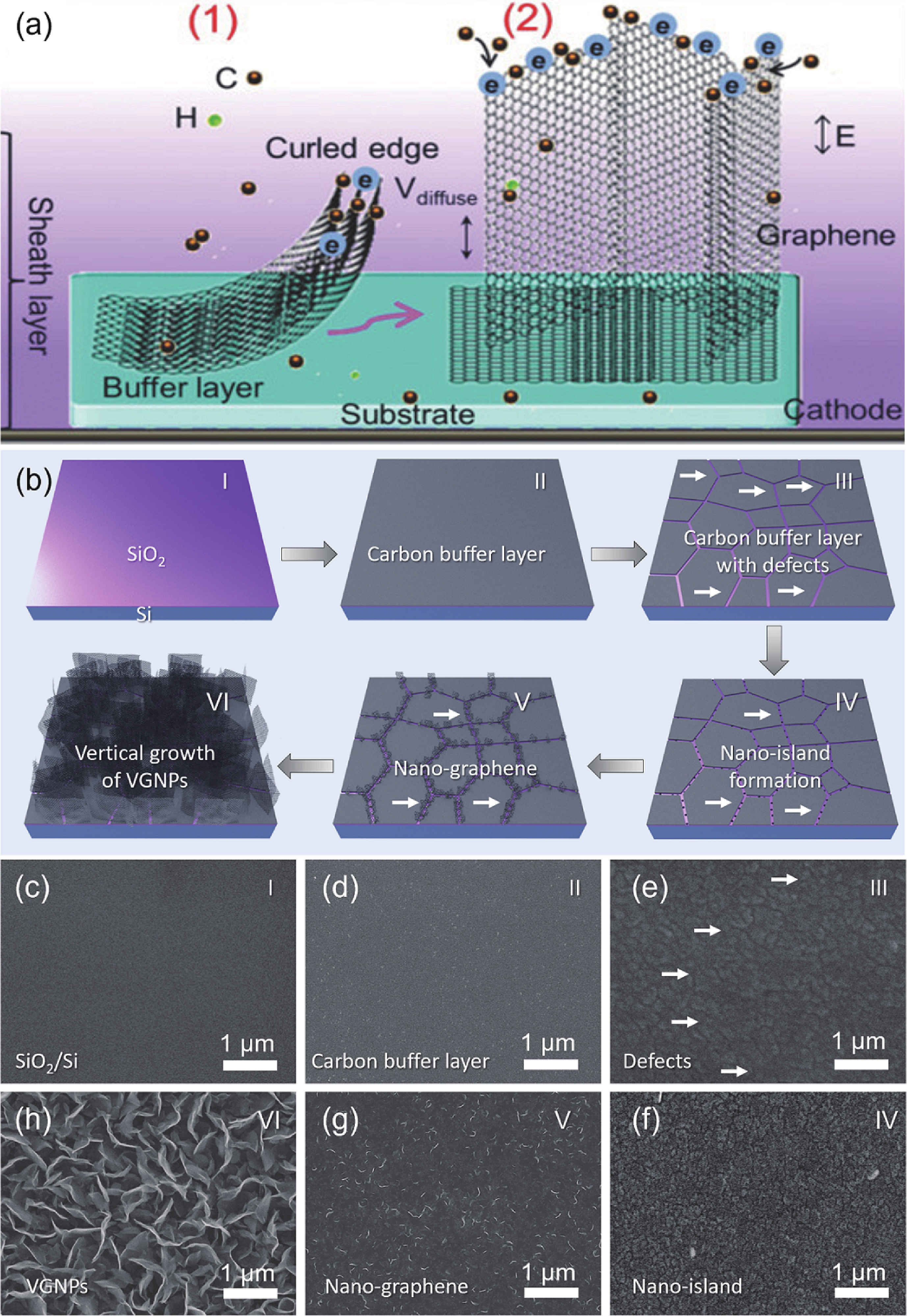
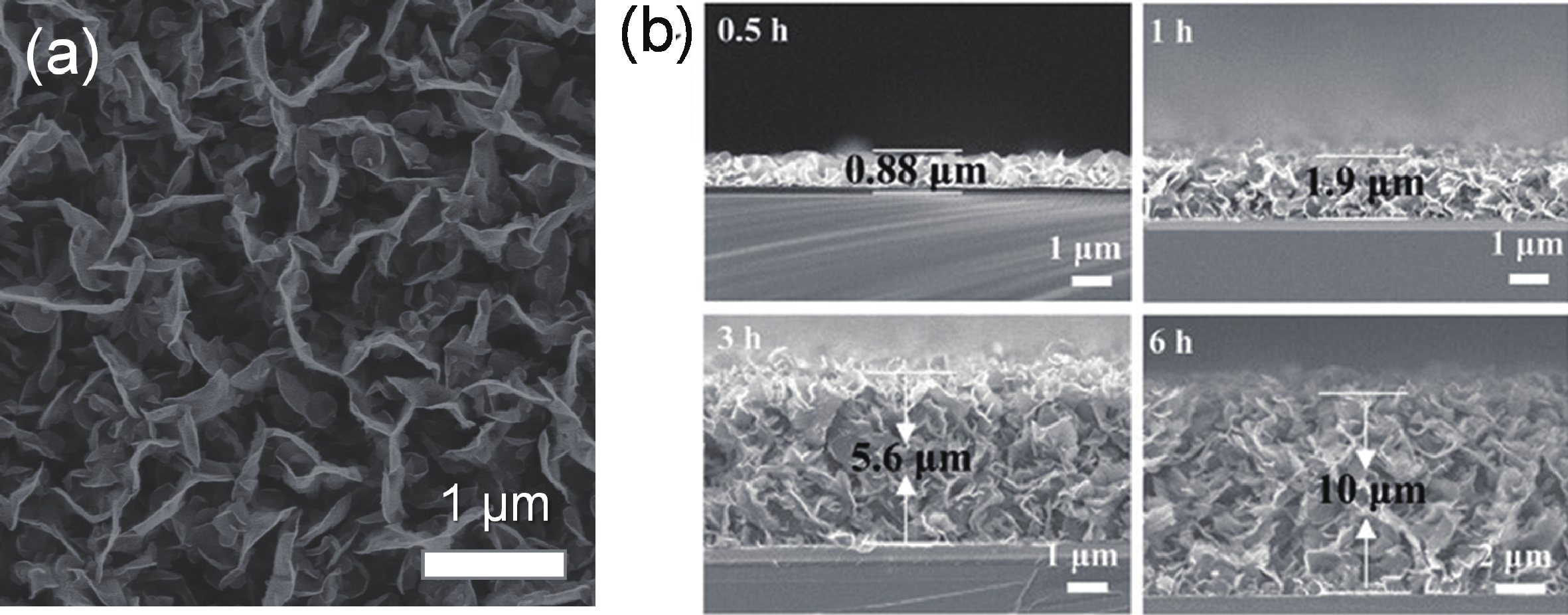
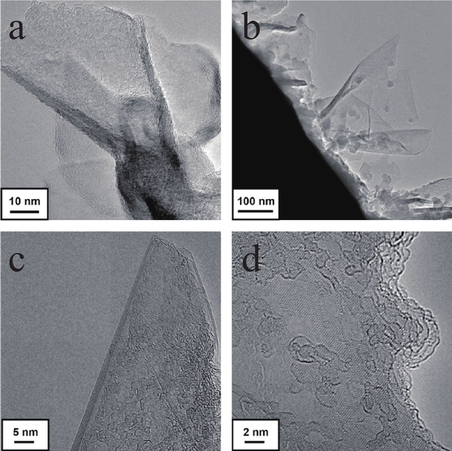
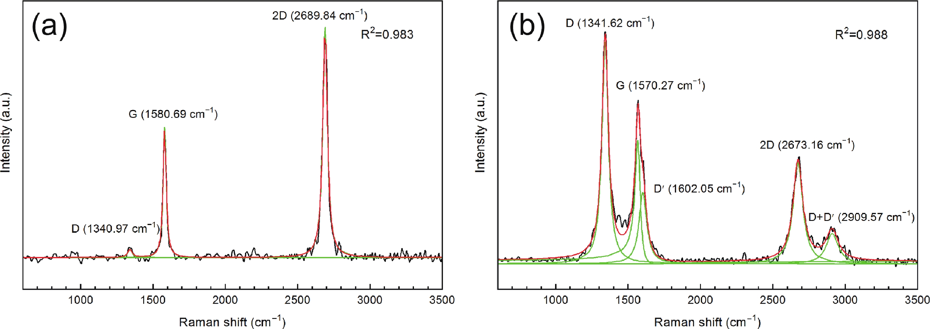

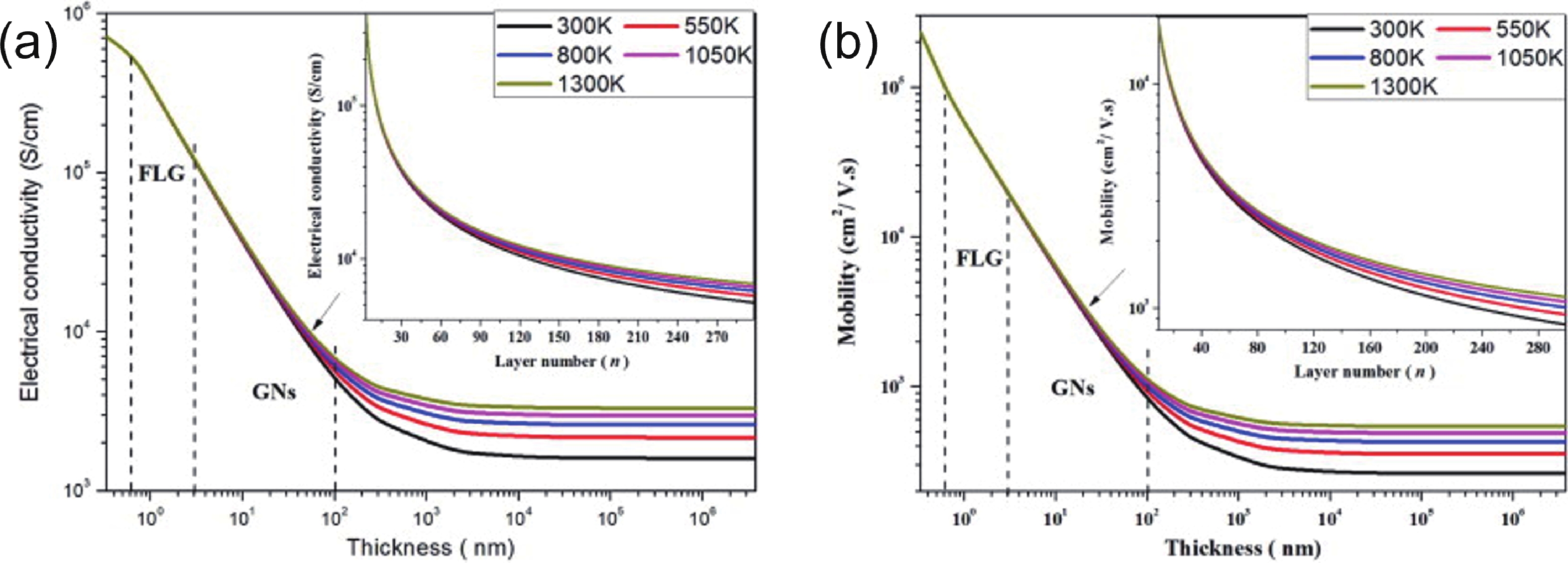
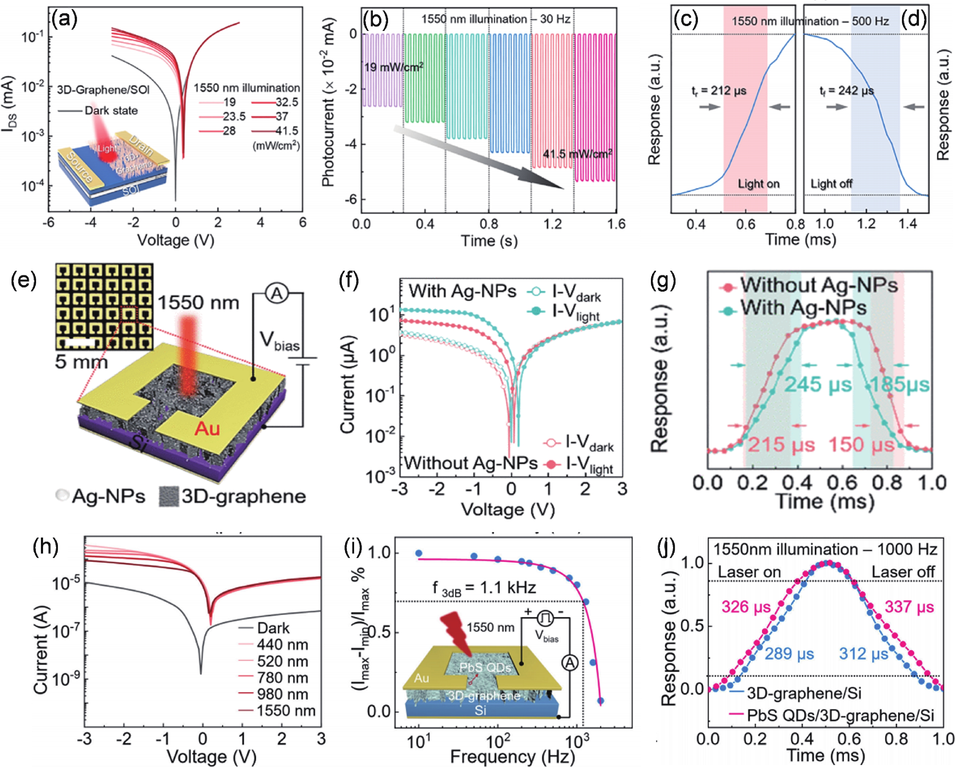
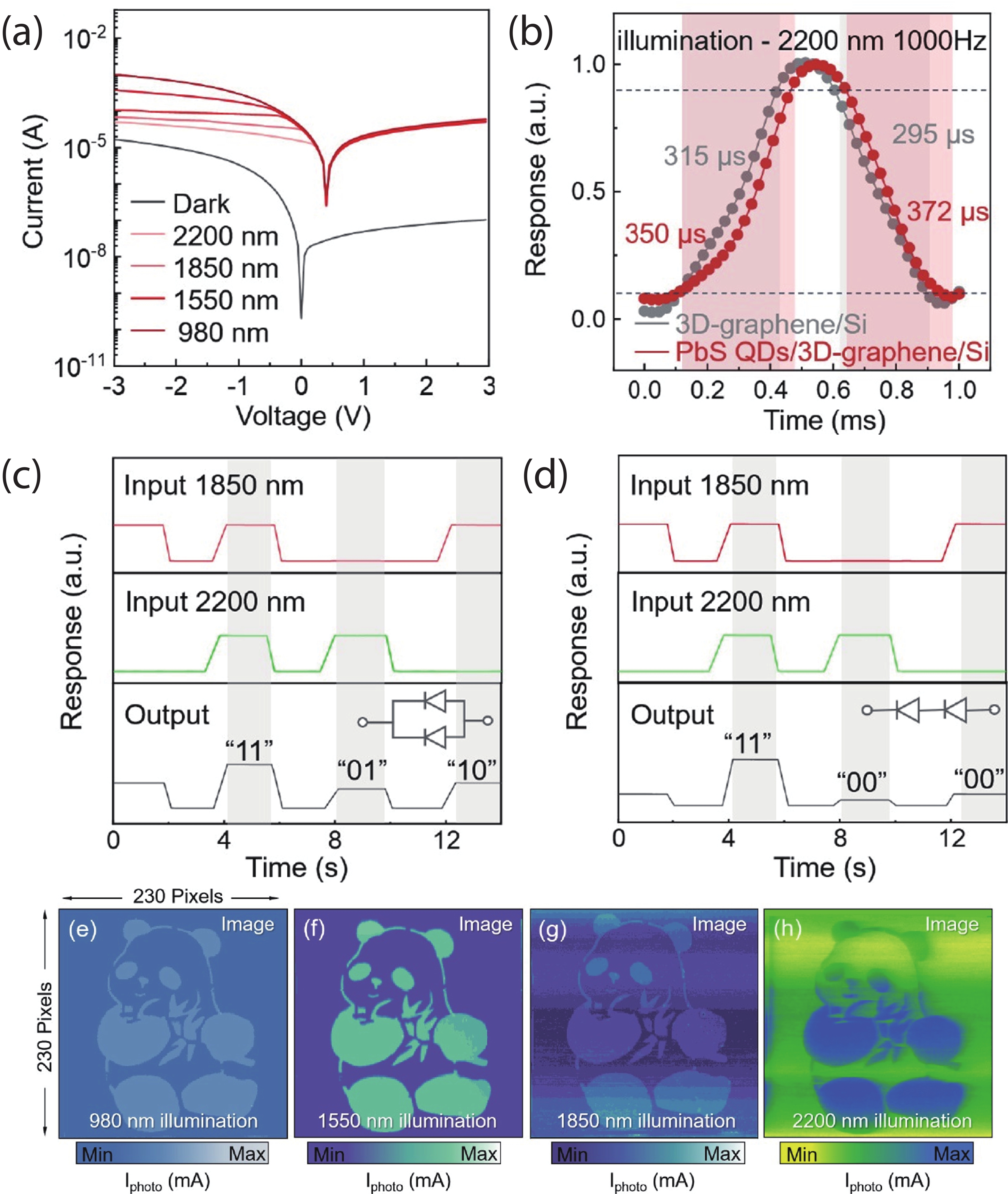
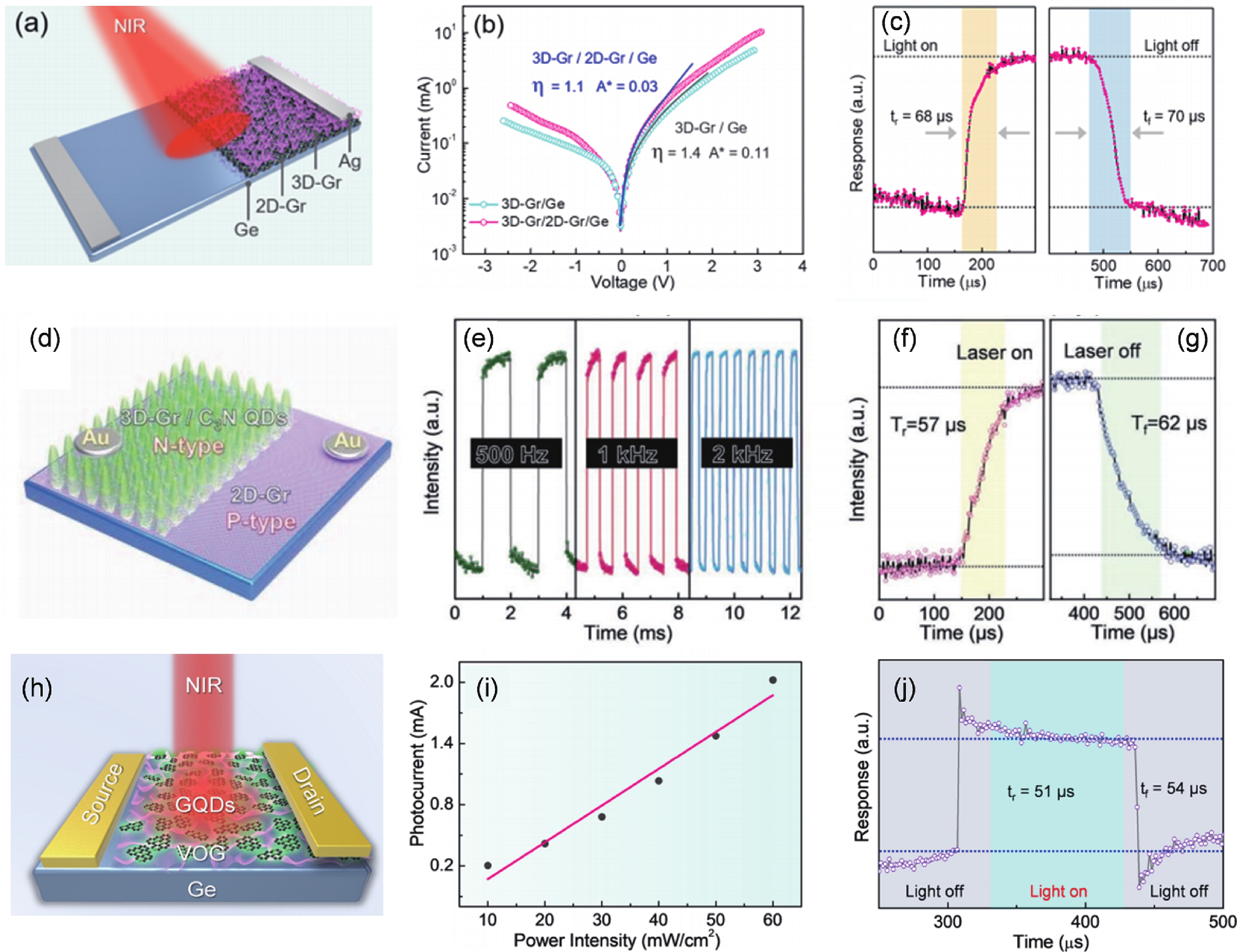
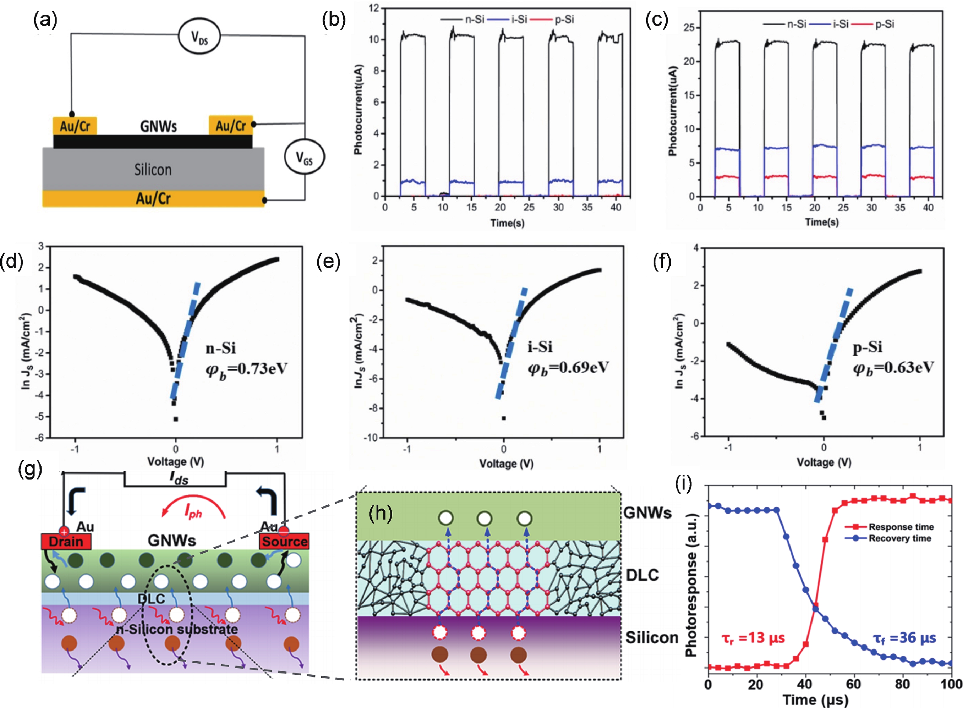

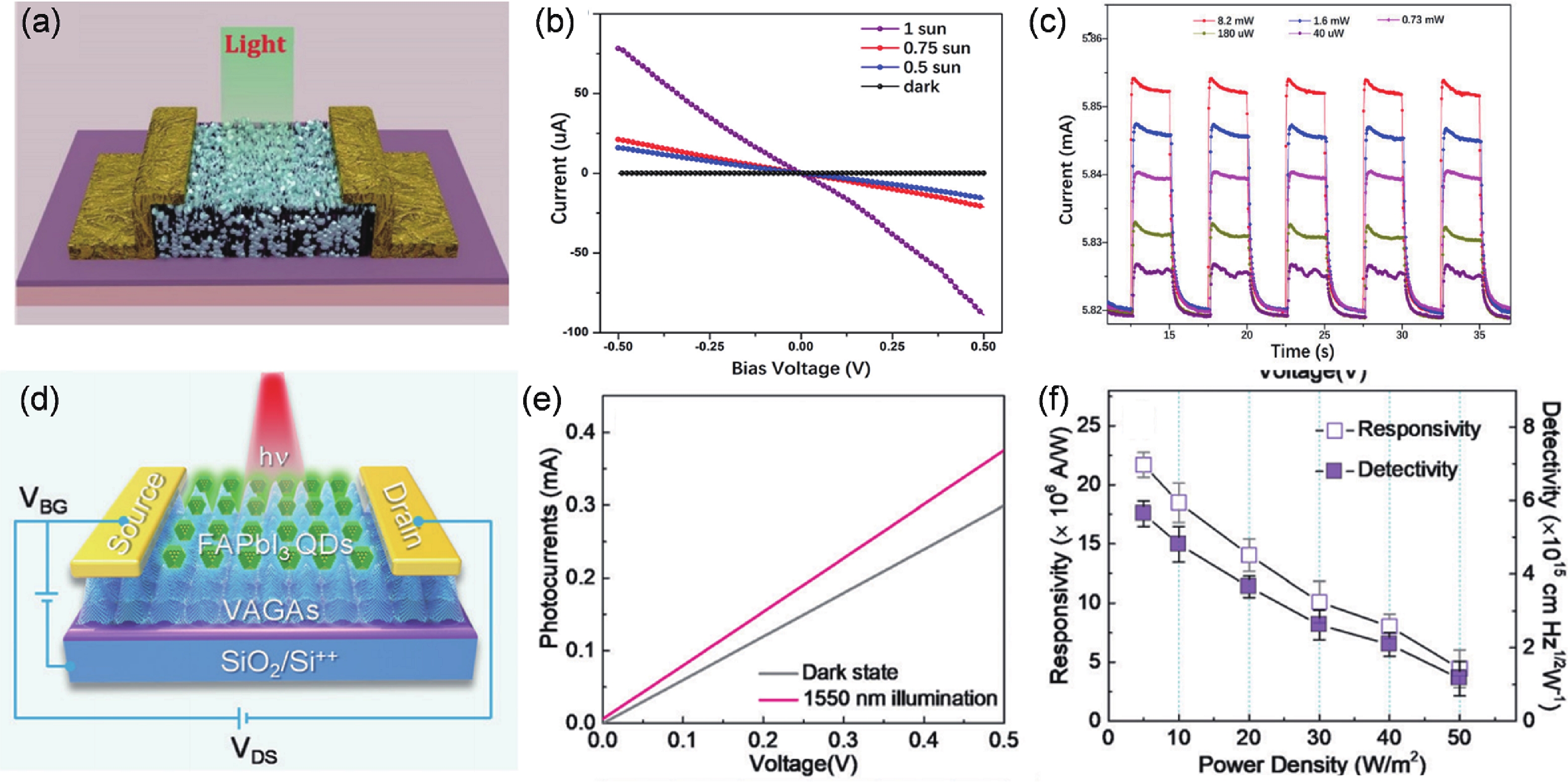
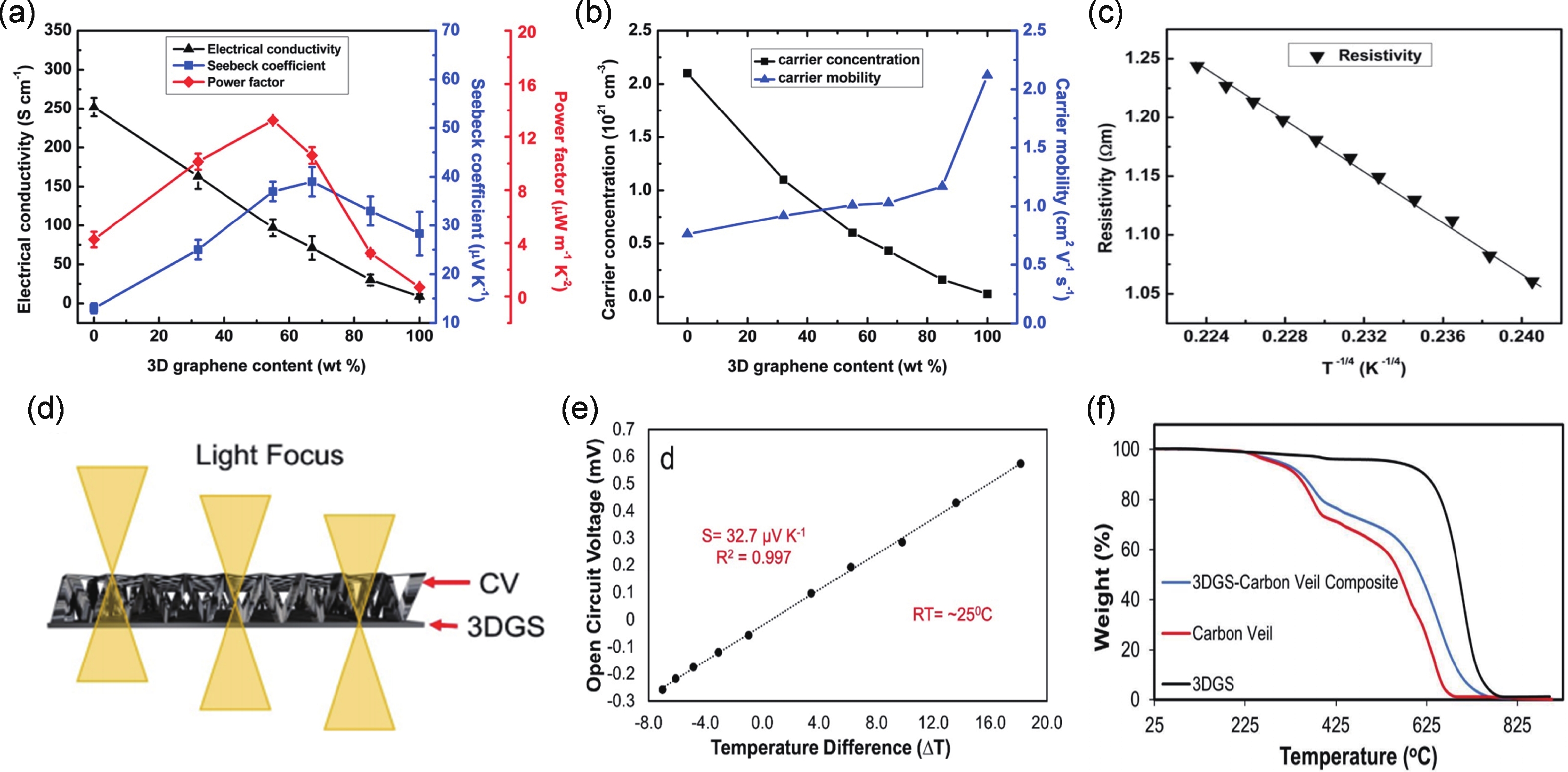
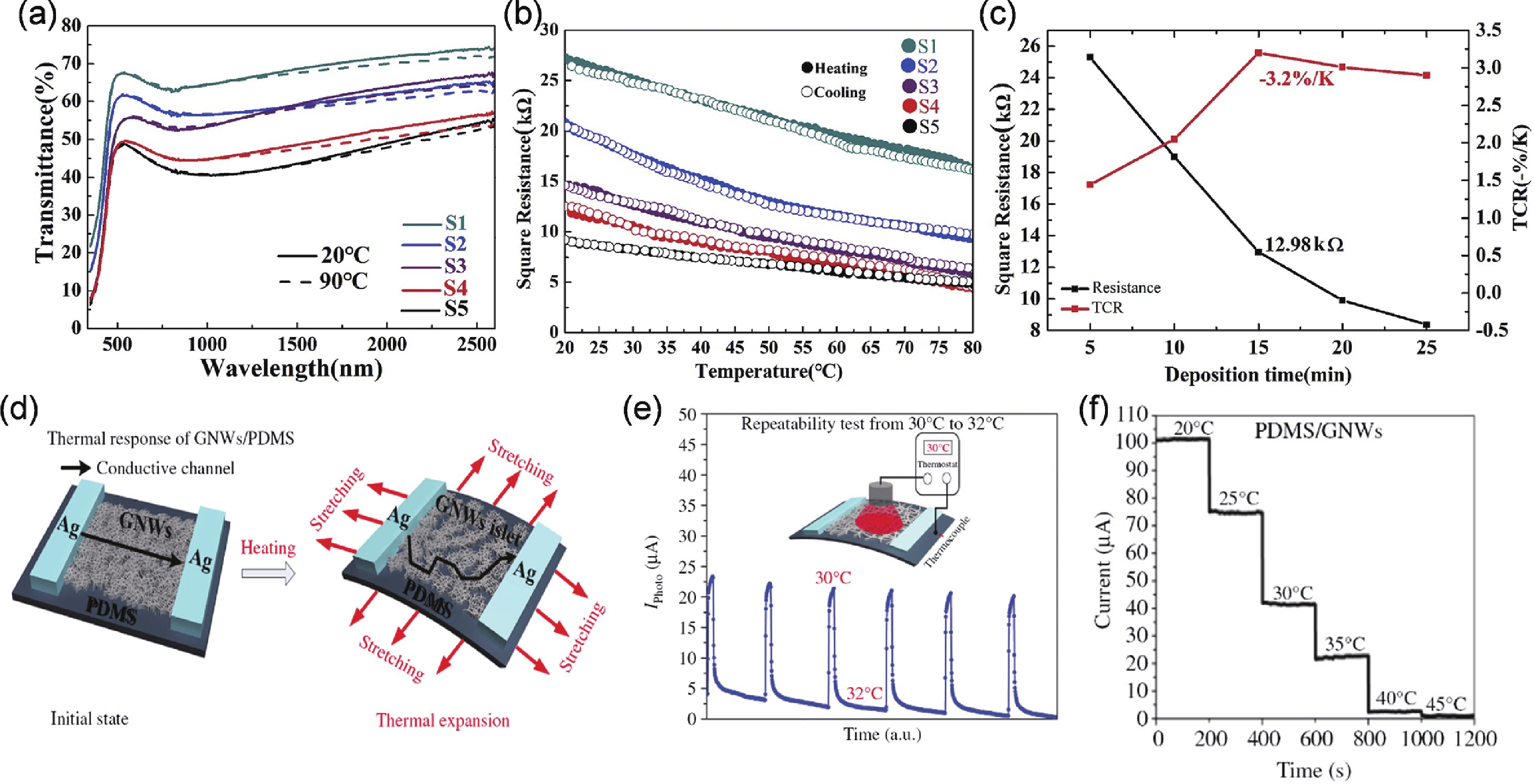
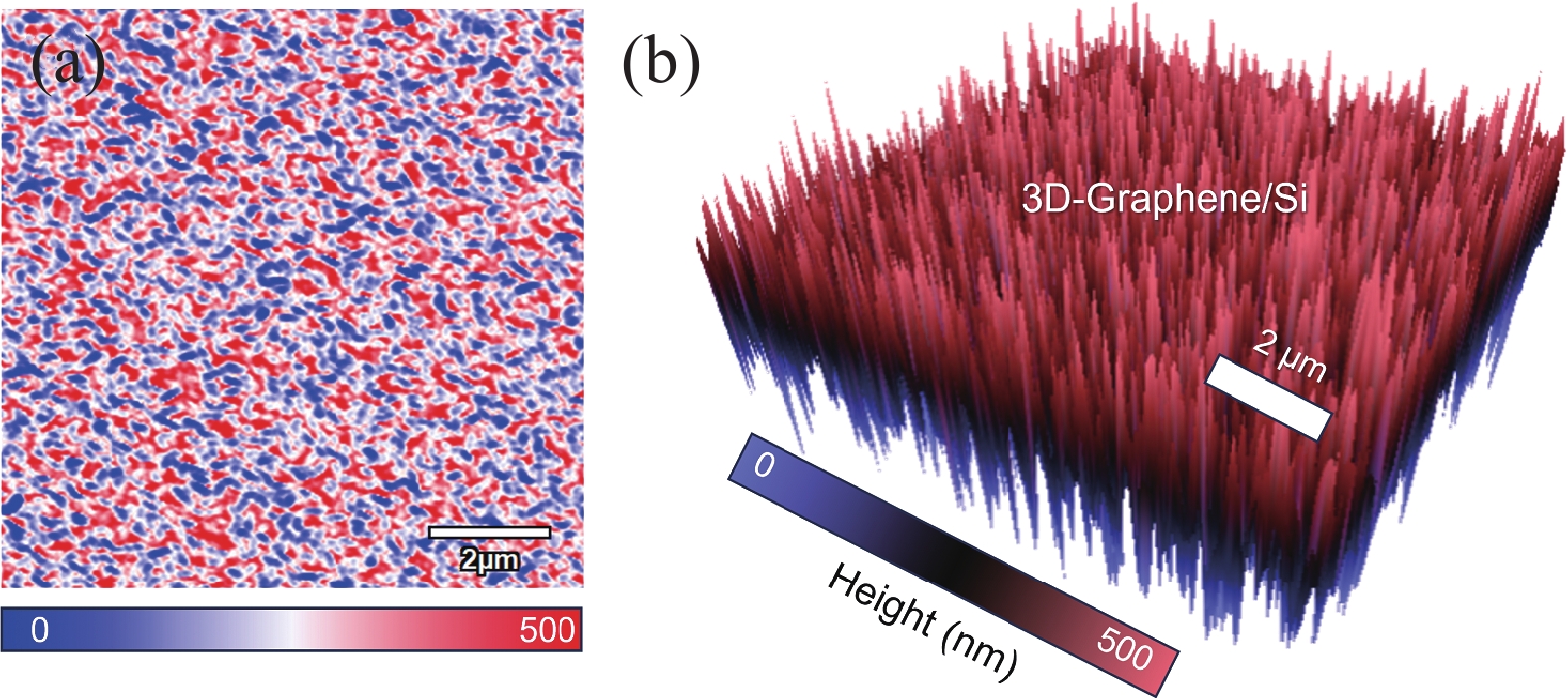
Table 1. The performance metrics, including responsivity, response time, wavelength, and detectivity for photodetectors fabricated using 3D-graphene.
| Device structure | Wavelength (nm) |
Rise time (tr) |
Fall time (tf) |
Responsivity (A/W) |
Detectivity (cm∙Hz1/2∙W−1) |
Reference |
| GrapheneNWs/planar-Si | 532 | 40 μs | − | 0.52 | 5.88 × 10¹³ | [92] |
| 3D-Gr/high-κ/Si | 1550 | 168 μs | 196 μs | 11. 2 | 5.9 × 10¹⁰ | [93] |
| 3D-Gr/SOI | 1550 | 212 μs | 242 μs | 27.4 | 1.37 × 10¹¹ | [72] |
| Ag-NPs/3D-Gr/Si | 1550 | 245 μs | 185 μs | 65.3 | 1.5 × 10¹⁰ | [96] |
| PbS QDs/3D-Gr/Si | 1550 | 326 μs | 337 μs | 13.7 | 1 × 10¹¹ | [87] |
| PbS QDs/3D-Gr/Si | 2200 | 350 μs | 372 μs | 52 | 6.8 × 10¹⁰ | [100] |
| 3D-Gr/2D-Gr/Ge | 1550 | 68 μs | 70 μs | 1.7 | 3.42 × 10¹⁴ | [101] |
| 3D-Gr/C3N QDs/2D-Gr/Ge | 1550 | 57 μs | 62 μs | 2.98 × 10⁷ | 1.04 × 10¹³ | [105] |
| GQDs/VOG/Ge | 1550 | 51 μs | 54 μs | 1.06 × 10⁶ | 2.11 × 10¹⁴ | [106] |
| GNWs/DLC/Si | 532 | 13 μs | 36 μs | 2.4 × 10³ | 1.07 × 10¹¹ | [127] |
| VG/ITO | 980 | 5.8 s | 6 s | 0.7 | − | [128] |
| FAPbI3 QDs/VAGAs | 1550 | 42 μs | 45 μs | 2.17 × 10⁷ | 5.64 × 10¹⁵ | [134] |
| CH3NH3PbIxCl3−x/GNWs | 633 | 50 ms | 290 ms | 2.02 × 10³ | 7.2 × 10¹⁰ | [133] |
 DownLoad: CSV
Table 2. The performance of 3D-graphene photodetectors is compared with other photodetectors.
| Detector type | Response speed |
Spectral response range |
Quantum efficiency |
Dark current | Flexibility | Cost |
| 3D-graphene photodetectors | Fast | UV−IR | Lower | Relatively high | Good | Low |
| 2D photoelectric sensors | Faster | Varies by material | Higher | Varies by material | Better | Higher |
| InGaAs photodetector | Fast | Near infrared | High | Low | Difference | High |
| HgTeCd photodetector | Faster | Near infrared−far Infrared | High | Low | Difference | High |
DownLoad: CSV
| [1] |
Liang S, Wang F F, Ma Z, et al. Asymmetric light excitation for photodetectors based on nanoscale semiconductors. ACS Nano, 2017, 11(1), 549 doi: 10.1021/acsnano.6b06598
|
| [2] |
Hu X, Wu J H, Wu M Z, et al. Recent developments of infrared photodetectors with low-dimensional inorganic nanostructures. Nano Res, 2022, 15(2), 805 doi: 10.1007/s12274-021-3634-2
|
| [3] |
Pan Q, Su M, Zhang Z Y, et al. Omnidirectional photodetectors based on spatial resonance asymmetric facade via a 3D self-standing strategy. Advanced Materials, 2020, 32, 1907280 doi: 10.1002/adma.201907280
|
| [4] |
Chen M, Wang Y X, Zhao Z R. Monolithic metamaterial-integrated graphene terahertz photodetector with wavelength and polarization selectivity. ACS Nano, 2022, 16(10), 17263 doi: 10.1021/acsnano.2c07968
|
| [5] |
Gayduchenko I, Xu S G, Alymov G, et al. Tunnel field-effect transistors for sensitive terahertz detection. Nat Commun, 2021, 12(1), 543 doi: 10.1038/s41467-020-20721-z
|
| [6] |
He X W, Wang X, Nanot S, et al. Photothermoelectric p-n junction photodetector with intrinsic broadband polarimetry based on macroscopic carbon nanotube films. ACS Nano, 2013, 7(8), 7271 doi: 10.1021/nn402679u
|
| [7] |
Li L L, Xu H, Li Z X, et al. CMOS-compatible tellurium/silicon ultra-fast near-infrared photodetector. Small, 2023, 19(42), 2303114 doi: 10.1002/smll.202303114
|
| [8] |
Wei B B, Zou B Q, Liu J X, et al. Polarization-sensitive photodetector based on quasi-1D (TaSe4)2I nanowire response to 10.6 µm. Adv Funct Materials, 2024, 34(30), 2315194 doi: 10.1002/adfm.202315194
|
| [9] |
He Z Y, Du X Y, Yu X, et al. Reverse-distribution phase featured gradient heterojunction: A universal strategy to realize high-performance near-infrared organic photodetectors for real-time arterial monitoring. Nano Energy, 2023, 114, 108673 doi: 10.1016/j.nanoen.2023.108673
|
| [10] |
Zhou Y C, Yang J, Bai L, et al. Flexible phase change hydrogels for mid-/low-temperature infrared stealth. Chemical Engineering Journal, 2022, 446, 137463 doi: 10.1016/j.cej.2022.137463
|
| [11] |
Zhou Z Q, Shen T, Wang P, et al. Low symmetric sub-wavelength array enhanced lensless polarization-sensitivity photodetector of germanium selenium. Sci Bull, 2023, 68(2), 173 doi: 10.1016/j.scib.2023.01.013
|
| [12] |
Wang F, Zhang T, Xie R, et al. Next-generation photodetectors beyond van der waals junctions. Adv Mater, 2024, 36(3), e2301197 doi: 10.1002/adma.202301197
|
| [13] |
Gao L F, Zhao Y M, Chang X H, et al. Emerging applications of MXenes for photodetection: Recent advances and future challenges. Mater Today, 2022, 61, 169 doi: 10.1016/j.mattod.2022.10.022
|
| [14] |
Pan X Y, Ding L M. Application of metal halide perovskite photodetectors. J Semicond, 2022, 43(2), 020203 doi: 10.1088/1674-4926/43/2/020203
|
| [15] |
Novoselov K S, Geim A K, Morozov S V, et al. Electric field effect in atomically thin carbon films. Science, 2004, 306(5696), 666 doi: 10.1126/science.1102896
|
| [16] |
Zhao C C, Liu Y Y, Wang D B, et al. High-performance self-driven broadband photoelectrochemical photodetector based on reduced graphene oxide/Bi2Te3 heterojunction. Nano Mater Sci, 2024, 6(6), 741 doi: 10.1016/j.nanoms.2023.12.008
|
| [17] |
Echtermeyer T J, Britnell L, Jasnos P K, et al. Strong plasmonic enhancement of photovoltage in graphene. Nat Commun, 2011, 2, 458 doi: 10.1038/ncomms1464
|
| [18] |
Chang H X, Wu H K. Graphene-based nanomaterials: Synthesis, properties, and optical and optoelectronic applications. Adv Funct Materials, 2013, 23(16), 1984 doi: 10.1002/adfm.201202460
|
| [19] |
Sinitskii A. A recipe for nanoporous graphene. Science, 2018, 360(6385), 154 doi: 10.1126/science.aat5117
|
| [20] |
Li P L, Wei W Y, Zhang M, et al. Wafer-scale growth of single-crystal graphene on vicinal Ge(001) substrate. Nano Today, 2020, 34, 100908 doi: 10.1016/j.nantod.2020.100908
|
| [21] |
Zhang X, Jing Q, Ao S, et al. Ultrasensitive field-effect biosensors enabled by the unique electronic properties of graphene. Small, 2020, 16(15), e1902820 doi: 10.1002/smll.201902820
|
| [22] |
Koepfli S M, Baumann M, Koyaz Y, et al. Metamaterial graphene photodetector with bandwidth exceeding 500 gigahertz. Science, 2023, 380(6650), 1169 doi: 10.1126/science.adg8017
|
| [23] |
Du S C, Lu W, Ali A, et al. A broadband fluorographene photodetector. Adv Mater, 2017, 29(22), 1700463 doi: 10.1002/adma.201700463
|
| [24] |
Biccari F, Gabelloni F, Burzi E, et al. Graphene-based electron transport layers in perovskite solar cells: A step-up for an efficient carrier collection. Adv Energy Mater, 2017, 7(22), 1701349 doi: 10.1002/aenm.201701349
|
| [25] |
Agresti A, Pescetelli S, Cinà L, et al. Efficiency and stability enhancement in perovskite solar cells by inserting lithium-neutralized graphene oxide as electron transporting layer. Adv Funct Materials, 2016, 26(16), 2686 doi: 10.1002/adfm.201504949
|
| [26] |
Du S C, Xie H, Yin J X, et al. Giant hot electron thermalization via stacking of graphene layers. Carbon, 2023, 203, 835 doi: 10.1016/j.carbon.2022.12.017
|
| [27] |
Sassi U, Parret R, Nanot S, et al. Graphene-based mid-infrared room-temperature pyroelectric bolometers with ultrahigh temperature coefficient of resistance. Nat Commun, 2017, 8, 14311 doi: 10.1038/ncomms14311
|
| [28] |
Nair R R, Blake P, Grigorenko A N, et al. Fine structure constant defines visual transparency of graphene. Science, 2008, 320(5881), 1308 doi: 10.1126/science.1156965
|
| [29] |
Elias D C, Nair R R, Mohiuddin T G, et al. Control of graphene’s properties by reversible hydrogenation: Evidence for graphane. Science, 2009, 323(5914), 610 doi: 10.1126/science.1167130
|
| [30] |
Castro E V, Novoselov K S, Morozov S V, et al. Biased bilayer graphene: Semiconductor with a gap tunable by the electric field effect. Phys Rev Lett, 2007, 99(21), 216802 doi: 10.1103/PhysRevLett.99.216802
|
| [31] |
Yin J B, Wang H, Peng H, et al. Selectively enhanced photocurrent generation in twisted bilayer graphene with van Hove singularity. Nat Commun, 2016, 7, 10699 doi: 10.1038/ncomms10699
|
| [32] |
Peng Y Y, Zhao W W, Ni F, et al. Forest-like laser-induced graphene film with ultrahigh solar energy utilization efficiency. ACS Nano, 2021, 15(12), 19490 doi: 10.1021/acsnano.1c06277
|
| [33] |
Zhang Q Q, You X, Tian L, et al. Fabrication and efficient electromagnetic waves attenuation of three-dimensional porous reduced graphene oxide/boron nitride/silicon carbide hierarchical structures. J Mater Sci Technol, 2023, 155, 192 doi: 10.1016/j.jmst.2022.12.056
|
| [34] |
Deng T, Zhang Z H, Liu Y X, et al. Three-dimensional graphene field-effect transistors as high-performance photodetectors. Nano Lett, 2019, 19(3), 1494 doi: 10.1021/acs.nanolett.8b04099
|
| [35] |
Olatomiwa A L, Adam T, Gopinath S C B, et al. Graphene synthesis, fabrication, characterization based on bottom-up and top-down approaches: An overview. J Semicond, 2022, 43(6), 061101 doi: 10.1088/1674-4926/43/6/061101
|
| [36] |
Shivananju B N, Yu W, Liu Y, et al. The roadmap of graphene-based optical biochemical sensors. Adv Funct Materials, 2016, 27, 1603918 doi: 10.1002/adfm.201603918
|
| [37] |
Cheng H H, Zhao F, Xue J L, et al. One single graphene oxide film for responsive actuation. ACS Nano, 2016, 10(10), 9529 doi: 10.1021/acsnano.6b04769
|
| [38] |
Fratzl P, Barth F G. Biomaterial systems for mechanosensing and actuation. Nature, 2009, 462(7272), 442 doi: 10.1038/nature08603
|
| [39] |
Ma T, Gao H L, Cong H P, et al. A bioinspired interface design for improving the strength and electrical conductivity of graphene-based fibers. Adv Mater, 2018, 30(15), 1706435 doi: 10.1002/adma.201706435
|
| [40] |
Stankovich S, Dikin D A, Dommett G H B, et al. Graphene-based composite materials. Nature, 2006, 442(7100), 282 doi: 10.1038/nature04969
|
| [41] |
Sadasivuni K K, Ponnamma D, Thomas S, et al. Evolution from graphite to graphene elastomer composites. Prog Polym Sci, 2014, 39(4), 749 doi: 10.1016/j.progpolymsci.2013.08.003
|
| [42] |
Li G Z, Huang B, Pan Z F, et al. Advances in three-dimensional graphene-based materials: Configurations, preparation and application in secondary metal (Li, Na, K, Mg, Al)-ion batteries. Energy Environ Sci, 2019, 12(7), 2030 doi: 10.1039/C8EE03014F
|
| [43] |
D’Apuzzo F, Piacenti A R, Giorgianni F, et al. Terahertz and mid-infrared plasmons in three-dimensional nanoporous graphene. Nat Commun, 2017, 8, 14885 doi: 10.1038/ncomms14885
|
| [44] |
Shi J L, Wang H F, Zhu X L, et al. The nanostructure preservation of 3D porous graphene: New insights into the graphitization and surface chemistry of non-stacked double-layer templated graphene after high-temperature treatment. Carbon, 2016, 103, 36 doi: 10.1016/j.carbon.2016.03.002
|
| [45] |
Ma Y F, Chen Y S. Three-dimensional graphene networks: Synthesis, properties and applications. Natl Sci Rev, 2015, 2(1), 40 doi: 10.1093/nsr/nwu072
|
| [46] |
Ando Y, Zhao X, Ohkohchi M. Production of petal-like graphite sheets by hydrogen arc discharge. Carbon, 1997, 35(1), 153 doi: 10.1016/S0008-6223(96)00139-X
|
| [47] |
Wu Y, Qiao P, Chong T, et al. Carbon nanowalls grown by microwave plasma enhanced chemical vapor deposition. Adv Mater, 2002, 14(1), 64 doi: 10.1002/1521-4095(20020104)14:1<64::AID-ADMA64>3.0.CO;2-G
|
| [48] |
Zhao J, Shaygan M, Eckert J, et al. A growth mechanism for free-standing vertical graphene. Nano Lett, 2014, 14(6), 3064 doi: 10.1021/nl501039c
|
| [49] |
Akhavan O, Ghaderi E, Rahighi R. Toward single-DNA electrochemical biosensing by graphene nanowalls. ACS Nano, 2012, 6(4), 2904 doi: 10.1021/nn300261t
|
| [50] |
Zhang L X, Sun Z, Qi J L, et al. Understanding the growth mechanism of vertically aligned graphene and control of its wettability. Carbon, 2016, 103, 339 doi: 10.1016/j.carbon.2016.03.029
|
| [51] |
Hojati-Talemi P, Simon G P. Field emission study of graphene nanowalls prepared by microwave-plasma method. Carbon, 2011, 49(8), 2875 doi: 10.1016/j.carbon.2011.03.004
|
| [52] |
Tang B, Wang S L, Zhang J, et al. Three-dimensional graphene monolith-based composite: Superiority in properties and applications. Int Mater Rev, 2018, 63(3), 204 doi: 10.1080/09506608.2017.1344377
|
| [53] |
Jin S X, Feng Y Y, Jia J C, et al. Three-dimensional N-doped carbon nanotube/graphene composite aerogel anode to develop high-power microbial fuel cell. Energy Environ Mater, 2023, 6(3), e12373 doi: 10.1002/eem2.12373
|
| [54] |
Yang Y, Liu T Y, Liao Q, et al. A three-dimensional nitrogen-doped graphene aerogel-activated carbon composite catalyst that enables low-cost microfluidic microbial fuel cells with superior performance. J Mater Chem A, 2016, 4(41), 15913 doi: 10.1039/C6TA05002F
|
| [55] |
Zhang Z Y, Li W Y, Yuen M F, et al. Hierarchical composite structure of few-layers MoS2 nanosheets supported by vertical graphene on carbon cloth for high-performance hydrogen evolution reaction. Nano Energy, 2015, 18, 196 doi: 10.1016/j.nanoen.2015.10.014
|
| [56] |
Ye S B, Feng J C. Towards three-dimensional, multi-functional graphene-based nanocomposite aerogels by hydrophobicity-driven absorption. J Mater Chem A, 2014, 2(27), 10365 doi: 10.1039/c4ta01392a
|
| [57] |
Zheng X L, Xiong X, Yang J W, et al. A strong and compressible three dimensional graphene/polyurushiol composite for efficient water cleanup. Chem Eng J, 2018, 333, 153 doi: 10.1016/j.cej.2017.09.146
|
| [58] |
Sun S M, Wang S, Li S D, et al. Asymmetric supercapacitors based on a NiCo2O4/three dimensional graphene composite and three dimensional graphene with high energy density. J Mater Chem A, 2016, 4(47), 18646 doi: 10.1039/C6TA07746C
|
| [59] |
Zhao X Y, Li X L, Zhang S L, et al. A three-dimensional sponge of graphene nanoribbons crosslinked by Fe3O4 nanoparticles for Li+ storage. J Mater Chem A, 2017, 5(45), 23592 doi: 10.1039/C7TA07874A
|
| [60] |
He M L, Wu L Y, Yu A L, et al. Surface functionalization of vertical graphene significantly enhances the energy storage capability for symmetric supercapacitors. Carbon, 2024, 216, 118511 doi: 10.1016/j.carbon.2023.118511
|
| [61] |
Ma J H, Wang P, Dong L, et al. Highly conductive, mechanically strong graphene monolith assembled by three-dimensional printing of large graphene oxide. J Colloid Interface Sci, 2019, 534, 12 doi: 10.1016/j.jcis.2018.08.096
|
| [62] |
Mo Y C, Yang K C, Lin J S, et al. CoSe2 anchored vertical graphene/macroporous carbon nanofibers used as multifunctional interlayers for high-performance lithium–sulfur batteries. J Mater Chem A, 2023, 11(12), 6349 doi: 10.1039/D2TA10020G
|
| [63] |
Wang S, Wang X, Sun C L, et al. Room-temperature fast assembly of 3D macroscopically porous graphene frameworks for binder-free compact supercapacitors with high gravimetric and volumetric capacitances. J Energy Chem, 2021, 61, 23 doi: 10.1016/j.jechem.2021.01.019
|
| [64] |
Rajackaitė E, Peckus D, Gudaitis R, et al. The evolution of properties with deposition time of vertical graphene nanosheets produced by microwave plasma-enhanced chemical vapor deposition. Surf Interfaces, 2021, 27, 101529 doi: 10.1016/j.surfin.2021.101529
|
| [65] |
Hiramatsu M, Shiji K, Amano H, et al. Fabrication of vertically aligned carbon nanowalls using capacitively coupled plasma-enhanced chemical vapor deposition assisted by hydrogen radical injection. Appl Phy Lett, 2004, 84(23), 4708 doi: 10.1063/1.1762702
|
| [66] |
Ma Y, Chaitoglou S, Farid G, et al. Supercapacitive performance of electrodes based on defective ZnO nanorods anchored on graphene nanowalls. Chem Eng J, 2024, 488, 151135 doi: 10.1016/j.cej.2024.151135
|
| [67] |
Qi Y, Deng B, Guo X, et al. Switching vertical to horizontal graphene growth using faraday cage-assisted PECVD approach for high-performance transparent heating device. Adv Mater, 2018, 30, 1704839 doi: 10.1002/adma.201704839
|
| [68] |
Li J R, Liu Z D, Guo Q L, et al. Controllable growth of vertically oriented graphene for high sensitivity gas detection. J Mater Chem C, 2019, 7(20), 5995 doi: 10.1039/C9TC01246J
|
| [69] |
Li J R, Guo Q L, Zhang N, et al. Direct integration of polycrystalline graphene on silicon as a photodetector via plasma-assisted chemical vapor deposition. J Mater Chem C, 2018, 6(36), 9682 doi: 10.1039/C8TC02646G
|
| [70] |
Xu S C, Wang S S, Chen Z, et al. Electric-field-assisted growth of vertical graphene arrays and the application in thermal interface materials. Adv Funct Materials, 2020, 30(34), 2003302 doi: 10.1002/adfm.202003302
|
| [71] |
Davami K, Shaygan M, Kheirabi N, et al. Synthesis and characterization of carbon nanowalls on different substrates by radio frequency plasma enhanced chemical vapor deposition. Carbon, 2014, 72, 372 doi: 10.1016/j.carbon.2014.02.025
|
| [72] |
He Z Y, Zhang G L, Zhang S, et al. Resonant nanocavity-enhanced graphene photodetectors on reflecting silicon-on-insulator wafers. Appl Phys Lett, 2021, 119(23), 232104 doi: 10.1063/5.0074703
|
| [73] |
Simionescu O G, Avram A, Adiaconiţă B, et al. Field-effect transistors based on single-layer graphene and graphene-derived materials. Micromachines, 2023, 14(6), 1096 doi: 10.3390/mi14061096
|
| [74] |
Seehra M S, Narang V, Geddam U K, et al. Correlation between X-ray diffraction and Raman spectra of 16 commercial graphene-based materials and their resulting classification. Carbon, 2017, 111, 380 doi: 10.1016/j.carbon.2016.10.010
|
| [75] |
Evlashin S, Svyakhovskiy S, Suetin N, et al. Optical and IR absorption of multilayer carbon nanowalls. Carbon, 2014, 70, 111 doi: 10.1016/j.carbon.2013.12.079
|
| [76] |
Zhang G L, Wang B K, Wu H J, et al. Nitrogen-doped 3D-graphene advances near-infrared photodetector for logic circuits and image sensors overcoming 2D limitations. Nano Lett, 2024, 24(33), 10062 doi: 10.1021/acs.nanolett.4c01917
|
| [77] |
Yu L Y, Zhang S, Zhang G L, et al. Dual-enhanced photodetectors combining graphene plasmonic nanoresonators with germanium-on-insulator optical cavities. IEEE Trans Electron Devices, 2022, 69(6), 3246 doi: 10.1109/TED.2022.3168528
|
| [78] |
Liu J, Li X Y, Wang Q, et al. A new 3D Dirac nodal-line semi-metallic graphene monolith for lithium ion battery anode materials. J Mater Chem A, 2018, 6(28), 13816 doi: 10.1039/C8TA04428G
|
| [79] |
Fang X Y, Yu X X, Zheng H M, et al. Temperature- and thickness-dependent electrical conductivity of few-layer graphene and graphene nanosheets. Phys Lett A, 2015, 379(37), 2245 doi: 10.1016/j.physleta.2015.06.063
|
| [80] |
Li H, Shi Y C, Shang H, et al. Atomic-scale tuning of graphene/cubic SiC Schottky junction for stable low-bias photoelectrochemical solar-to-fuel conversion. ACS Nano, 2020, 14(4), 4905 doi: 10.1021/acsnano.0c00986
|
| [81] |
Bai Z Q, Xiao Y, Luo Q, et al. Highly tunable carrier tunneling in vertical graphene-WS2-graphene van der waals heterostructures. ACS Nano, 2022, 16(5), 7880 doi: 10.1021/acsnano.2c00536
|
| [82] |
Lu Y H, Feng S R, Wu Z Q, et al. Broadband surface plasmon resonance enhanced self-powered graphene/GaAs photodetector with ultrahigh detectivity. Nano Energy, 2018, 47, 140 doi: 10.1016/j.nanoen.2018.02.056
|
| [83] |
Heo J H, Shin D H, Kim S, et al. Highly efficient CH3NH3PbI3 perovskite solar cells prepared by AuCl3-doped graphene transparent conducting electrodes. Chem Eng J, 2017, 323, 153 doi: 10.1016/j.cej.2017.04.097
|
| [84] |
Li H, Wu J B, Ran F R, et al. Interfacial interactions in van der waals heterostructures of MoS2 and graphene. ACS Nano, 2017, 11(11), 11714 doi: 10.1021/acsnano.7b07015
|
| [85] |
Shao Q G, Qi H, Li C, et al. Recent progress of gr/Si Schottky photodetectors. Electron Mater Lett, 2023, 19(2), 121 doi: 10.1007/s13391-022-00384-2
|
| [86] |
Riazimehr S, Kataria S, Bornemann R, et al. High photocurrent in gated graphene-silicon hybrid photodiodes. ACS Photonics, 2017, 4(6), 1506 doi: 10.1021/acsphotonics.7b00285
|
| [87] |
Zhang S, Zhang G L, Zheng L, et al. High-performance near-infrared photodetector by integration of PbS quantum dots with 3D-graphene. IEEE Electron Device Lett, 2023, 44(8), 1240 doi: 10.1109/LED.2023.3288140
|
| [88] |
Zhao Y, Tsai T Y, Wu G, et al. Graphene/SnS2 van der waals photodetector with high photoresponsivity and high photodetectivity for broadband 365-2240 nm detection. ACS Appl Mater Interfaces, 2021, 13(39), 47198 doi: 10.1021/acsami.1c11534
|
| [89] |
Zhang X K, Kang Z, Gao L, et al. Molecule-upgraded van der waals contacts for Schottky-barrier-free electronics. Adv Mater, 2021, 33(45), e2104935 doi: 10.1002/adma.202104935
|
| [90] |
Sun L, Zhu L F, Zhang C L, et al. Mechanical manipulation of silicon-based Schottky diodes via flexoelectricity. Nano Energy, 2021, 83, 105855 doi: 10.1016/j.nanoen.2021.105855
|
| [91] |
Li L, Fan Z Y. Optoelectronic materials and devices. Small Meth, 2024, 8(2), 2301632 doi: 10.1002/smtd.202301632
|
| [92] |
Shen J, Liu X Z, Song X F, et al. High-performance Schottky heterojunction photodetector with directly grown graphene nanowalls as electrodes. Nanoscale, 2017, 9(18), 6020 doi: 10.1039/C7NR00573C
|
| [93] |
He Z Y, Zhang S, Zheng L, et al. Si-based NIR tunneling heterojunction photodetector with interfacial engineering and 3D-graphene integration. IEEE Electron Device Lett, 2022, 43(11), 1818 doi: 10.1109/LED.2022.3203474
|
| [94] |
Kuznetsov A I, Miroshnichenko A E, Brongersma M L, et al. Optically resonant dielectric nanostructures. Science, 2016, 354(6314), aag2472 doi: 10.1126/science.aag2472
|
| [95] |
Tai S P, Wu Y, Shieh D B, et al. Molecular imaging of cancer cells using plasmon-resonant-enhanced third-harmonic-generation in silver nanoparticles. Adv Mater, 2007, 19(24), 4520 doi: 10.1002/adma.200602213
|
| [96] |
Zhang G L, Zhang S, Zheng L, et al. Localized surface plasmon resonance enables Si-based near-infrared photodetector. IEEE Trans Electron Devices, 2023, 70(10), 5497 doi: 10.1109/TED.2023.3303148
|
| [97] |
Liu Y H, Li F H, Huang H, et al. Optoelectronic and photocatalytic properties of I–III–VI QDs: Bridging between traditional and emerging new QDs. J Semicond, 2020, 41(9), 091701 doi: 10.1088/1674-4926/41/9/091701
|
| [98] |
Marino E, Sciortino A, Berkhout A, et al. Simultaneous photonic and excitonic coupling in spherical quantum dot supercrystals. ACS Nano, 2020, 14(10), 13806 doi: 10.1021/acsnano.0c06188
|
| [99] |
Pang X H, Bian H J, Wang W J, et al. A bio-chemical application of N-GQDs and g-C3N4 QDs sensitized TiO2 nanopillars for the quantitative detection of pcDNA3-HBV. Biosens Bioelectron, 2017, 91, 456 doi: 10.1016/j.bios.2016.12.059
|
| [100] |
Wu H J, Liu Z Y, Wang B K, et al. Integration of PbS quantum dots with 3D-graphene for self-powered broadband photodetectors in image sensors. ACS Photonics, 2024, 11(3), 1342 doi: 10.1021/acsphotonics.3c01803
|
| [101] |
Zhao M H, Xue Z Y, Zhu W, et al. Interface engineering-assisted 3D-graphene/germanium heterojunction for high-performance photodetectors. ACS Appl Mater Interfaces, 2020, 12(13), 15606 doi: 10.1021/acsami.0c02485
|
| [102] |
Sinha D, Lee J U. Ideal graphene/silicon Schottky junction diodes. Nano Lett, 2014, 14(8), 4660 doi: 10.1021/nl501735k
|
| [103] |
Xu Y, Cheng C, Du S C, et al. Contacts between two- and three-dimensional materials: Ohmic, Schottky, and p-n heterojunctions. ACS Nano, 2016, 10(5), 4895 doi: 10.1021/acsnano.6b01842
|
| [104] |
Liu X Z, Zhou Q, Luo S, et al. Infrared photodetector based on the photothermionic effect of graphene-nanowall/silicon heterojunction. ACS Appl Mater Interfaces, 2019, 11(19), 17663 doi: 10.1021/acsami.9b03329
|
| [105] |
Feng X Q, He Z Y, Liu Z D, et al. Intact vertical 3D–0D–2D carbon-based p–n junctions for use in high-performance photodetectors. Adv Opt Mater, 2021, 9(16), 2100387 doi: 10.1002/adom.202100387
|
| [106] |
Zhu W, Xue Z Y, Wang G, et al. Graphene quantum dot-decorated vertically oriented graphene/germanium heterojunctions for near-infrared photodetectors. ACS Appl Nano Mater, 2020, 3(7), 6915 doi: 10.1021/acsanm.0c01258
|
| [107] |
Fang H H, Hu W D. Photogating in low dimensional photodetectors. Adv Sci, 2017, 4(12), 1700323 doi: 10.1002/advs.201700323
|
| [108] |
Long M S, Wang P, Fang H H, et al. Progress, challenges, and opportunities for 2D material based photodetectors. Adv Funct Materials, 2019, 29(19), 1803807 doi: 10.1002/adfm.201803807
|
| [109] |
Sukhovatkin V, Hinds S, Brzozowski L, et al. Colloidal quantum-dot photodetectors exploiting multiexciton generation. Science, 2009, 324(5934), 1542 doi: 10.1126/science.1173812
|
| [110] |
Huijser A, Savenije T J, Kotlewski A, et al. Efficient light-harvesting layers of homeotropically aligned porphyrin derivatives. Adv Mater, 2006, 18(17), 2234 doi: 10.1002/adma.200600045
|
| [111] |
Zhang Z, Jia F A, Kong F H, et al. Chloride adsorbates enhance the photocarrier separation and promote the bio-syngas evolution. Small, 2023, 19(21), e2300810 doi: 10.1002/smll.202300810
|
| [112] |
Ghosh C, Dey A, Biswas I, et al. CuO–TiO2 based self-powered broad band photodetector. Nano Energy, 2020, 70, 104518 doi: 10.1016/j.nanoen.2020.104518
|
| [113] |
Ghosh C, Dey A, Biswas I, et al. CuO-TiO2 based self-powered broad band photodetector. Nano Mater Sci, 2024, 6(3), 345 doi: 10.1016/j.nanoms.2023.11.003
|
| [114] |
Niu W Z, Moehl T, Cui W, et al. Extended light harvesting with dual Cu2O-based photocathodes for high efficiency water splitting. Adv Energy Mater, 2018, 8(10), 1702323 doi: 10.1002/aenm.201702323
|
| [115] |
Tang H Y, Anwar T, Jang M S, et al. Light-intensity switching of graphene/WSe2 synaptic devices. Adv Sci, 2024, 11(24), e2309876 doi: 10.1002/advs.202309876
|
| [116] |
Wang W H, Du R X, Sun L T, et al. Ultrasensitive graphene position-sensitive detector induced by synergistic effects of charge injection and interfacial gating. Nanophotonics, 2020, 9(8), 2531 doi: 10.1515/nanoph-2020-0053
|
| [117] |
Liu F Z, Kar S. Quantum carrier reinvestment-induced ultrahigh and broadband photocurrent responses in graphene-silicon junctions. ACS Nano, 2014, 8(10), 10270 doi: 10.1021/nn503484s
|
| [118] |
Ma Z Y, Li G, Zhang X L, et al. High-performance and broadband photodetection of bicrystalline (GaN)1-x(ZnO)x solid solution nanowires via crystal defect engineering. J Mater Sci Technol, 2021, 85, 255 doi: 10.1016/j.jmst.2021.01.020
|
| [119] |
Srisonphan S, Jung Y S, Kim H K. Metal-oxide-semiconductor field-effect transistor with a vacuum channel. Nat Nanotechnol, 2012, 7(8), 504 doi: 10.1038/nnano.2012.107
|
| [120] |
Luo H W, Yu C M, Liu Z T, et al. Remarkable enhancement of charge carrier mobility of conjugated polymer field-effect transistors upon incorporating an ionic additive. Sci Adv, 2016, 2(5), e1600076 doi: 10.1126/sciadv.1600076
|
| [121] |
Sun H T, Mei L, Liang J F, et al. Three-dimensional holey-graphene/niobia composite architectures for ultrahigh-rate energy storage. Science, 2017, 356(6338), 599 doi: 10.1126/science.aam5852
|
| [122] |
Wang H C, Fu Y Q. Graphene-nanowalls/silicon hybrid heterojunction photodetectors. Carbon, 2020, 162, 181 doi: 10.1016/j.carbon.2020.02.023
|
| [123] |
Liu H Y, Sun F, Li X Y, et al. g-C3N4/TiO2/ZnIn2S4 graphene aerogel photocatalysts with double S-scheme heterostructure for improving photocatalytic multifunctional performances. Compos Part B Eng, 2023, 259, 110746 doi: 10.1016/j.compositesb.2023.110746
|
| [124] |
Li M M, Wang Y, Yang C C, et al. In situ grown Co3O4 nanocubes on N-doped graphene as a synergistic hybrid for applications in nickel metal hydride batteries. Int J Hydrog Energy, 2018, 43(39), 18421 doi: 10.1016/j.ijhydene.2018.08.054
|
| [125] |
Guo S H, Zhang B C, Zhang X L, et al. Non-noble-metal plasmonic parabolic membrane with "pearl necklace" structure for enhanced hydrogen production based on light concentration effect. Chem Eng J, 2024, 493, 152708 doi: 10.1016/j.cej.2024.152708
|
| [126] |
Meng J H, Liu X, Zhang X W, et al. Interface engineering for highly efficient graphene-on-silicon Schottky junction solar cells by introducing a hexagonal boron nitride interlayer. Nano Energy, 2016, 28, 44 doi: 10.1016/j.nanoen.2016.08.028
|
| [127] |
Yang J, Tang L L, Luo W, et al. Interface engineering of a silicon/graphene heterojunction photodetector via a diamond-like carbon interlayer. ACS Appl Mater Interfaces, 2021, 13(3), 4692 doi: 10.1021/acsami.0c18850
|
| [128] |
Yang J W, Liu Y D, Ci H N, et al. High-performance 3D vertically oriented graphene photodetector using a floating indium tin oxide channel. Sensors, 2022, 22(3), 959 doi: 10.3390/s22030959
|
| [129] |
Qiao H, Li Z J, Huang Z Y, et al. Self-powered photodetectors based on 0D/2D mixed dimensional heterojunction with black phosphorus quantum dots as hole accepters. Appl Mater Today, 2020, 20, 100765 doi: 10.1016/j.apmt.2020.100765
|
| [130] |
Lan G L, Nong J P, Jin W F, et al. Enhanced UV photoresponse employing 3D graphene nanowalls/SnO2 nanocomposite film. Surf Coat Technol, 2019, 359, 90 doi: 10.1016/j.surfcoat.2018.12.052
|
| [131] |
Gao Y, Zhao C, Pu K, et al. Low-voltage-modulated perovskite/organic dual-band photodetectors for visible and near-infrared imaging. Sci Bull, 2022, 67(19), 1982 doi: 10.1016/j.scib.2022.09.007
|
| [132] |
Ahmad A A, Al-Bataineh Q M, Migdadi A B. Nanocomposite superstructure of zinc oxide mesocrystal/reduced graphene oxide with effective photoconductivity. J Semicond, 2024, 45(11), 112701 doi: 10.1088/1674-4926/24060019
|
| [133] |
Zhou D H, Yu L Y, Zhu P, et al. Lateral structured phototransistor based on mesoscopic graphene/perovskite heterojunctions. Nanomaterials, 2021, 11(3), 641 doi: 10.3390/nano11030641
|
| [134] |
Feng X Q, He Z Y, Zhu W, et al. Perovskite quantum dots integrated with vertically aligned graphene toward ambipolar multifunctional photodetectors. J Mater Chem C, 2021, 9(2), 609 doi: 10.1039/D0TC04932H
|
| [135] |
Yang H, Tan C W, Deng C Y, et al. Bolometric effect in Bi2O2Se photodetectors. Small, 2019, 15(43), e1904482 doi: 10.1002/smll.201904482
|
| [136] |
Guo X H, Lu X W, Jiang P, et al. Touchless thermosensation enabled by flexible infrared photothermoelectric detector for temperature prewarning function of electronic skin. Adv Mater, 2024, 36(23), e2313911 doi: 10.1002/adma.202313911
|
| [137] |
Xiao Y, Zhao L D. Seeking new, highly effective thermoelectrics. Science, 2020, 367(6483), 1196 doi: 10.1126/science.aaz9426
|
| [138] |
Zhao L D, Lo S H, Zhang Y S, et al. Ultralow thermal conductivity and high thermoelectric figure of merit in SnSe crystals. Nature, 2014, 508(7496), 373 doi: 10.1038/nature13184
|
| [139] |
Wei M, Li H B, Nisar M, et al. The synergistic effect of hole co-doping on carrier transports and phonon tuning in Sb2Te3 flexible thermoelectric thin film. Chem Eng J, 2024, 495, 153185 doi: 10.1016/j.cej.2024.153185
|
| [140] |
Li Y Y, Liu G H, Cao T F, et al. Enhanced thermoelectric properties of Cu2SnSe3 by (Ag, In)-co-doping. Adv Funct Materials, 2016, 26(33), 6025 doi: 10.1002/adfm.201601486
|
| [141] |
Wang L M, Bi H, Yao Q, et al. Three-dimensional tubular graphene/polyaniline composites as high-performance elastic thermoelectrics. Compos Sci Technol, 2017, 150, 135 doi: 10.1016/j.compscitech.2017.07.001
|
| [142] |
Yao Q, Chen L D, Zhang W Q, et al. Enhanced thermoelectric performance of single-walled carbon nanotubes/polyaniline hybrid nanocomposites. ACS Nano, 2010, 4(4), 2445 doi: 10.1021/nn1002562
|
| [143] |
Peng H S. Aligned carbon nanotube/polymer composite films with robust flexibility, high transparency, and excellent conductivity. J Am Chem Soc, 2008, 130(1), 42 doi: 10.1021/ja078267m
|
| [144] |
Kondapalli V K R, Akinboye O I, Zhang Y, et al. Three-dimensional graphene sheet-carbon veil thermoelectric composite with microinterfaces for energy applications. ACS Appl Mater Interfaces, 2024, 16(10), 13150 doi: 10.1021/acsami.3c19605
|
| [145] |
Chen C H, Yi X J, Zhao X R, et al. Characterizations of VO2- based uncooled microbolometer linear array. Sens Actuat A Phys, 2001, 90(3), 212 doi: 10.1016/S0924-4247(01)00495-2
|
| [146] |
Wang B, Lai J J, Li H, et al. Nanostructured vanadium oxide thin film with high TCR at room temperature for microbolometer. Infrared Phys Technol, 2013, 57, 8 doi: 10.1016/j.infrared.2012.10.006
|
| [147] |
Dai J, Wang X Z, He S W, et al. Low temperature fabrication of VO x thin films for uncooled IR detectors by direct current reactive magnetron sputtering method. Infrared Phys Technol, 2008, 51(4), 287 doi: 10.1016/j.infrared.2007.12.002
|
| [148] |
Wei Z Y, Yang F, Bi K D, et al. Thermal transport properties of all-sp2 three-dimensional graphene: Anisotropy, size and pressure effects. Carbon, 2017, 113, 212 doi: 10.1016/j.carbon.2016.11.055
|
| [149] |
Lv P, Tan X W, Yu K H, et al. Super-elastic graphene/carbon nanotube aerogel: A novel thermal interface material with highly thermal transport properties. Carbon, 2016, 99, 222 doi: 10.1016/j.carbon.2015.12.026
|
| [150] |
Iglesias J M, Martín M J, Pascual E, et al. Hot carrier and hot phonon coupling during ultrafast relaxation of photoexcited electrons in graphene. Appl Phy Lett, 2016, 108(4), 043105 doi: 10.1063/1.4940902
|
| [151] |
Tran M D, Lee S G, Jeon S, et al. Decelerated hot carrier cooling in graphene via nondissipative carrier injection from MoS2. ACS Nano, 2020, 14(10), 13905 doi: 10.1021/acsnano.0c06311
|
| [152] |
Xu C, Liu G W, Li M, et al. Optical switching and nanothermochromic studies of VO2(M) nanoparticles prepared by mild thermolysis method. Mater Des, 2020, 187, 108396 doi: 10.1016/j.matdes.2019.108396
|
| [153] |
Wu B M, Zhang Z Y, Chen B X, et al. One-step rolling fabrication of VO2 tubular bolometers with polarization-sensitive and omnidirectional detection. Sci Adv, 2023, 9(42), eadi7805 doi: 10.1126/sciadv.adi7805
|
| [154] |
Lu Y, Zhang H, Wan D Y. CVD preparation of vertical graphene nanowalls/VO2(B) composite films with superior thermal sensitivity in uncooled infrared detector. J Materiomics, 2020, 6(2), 280 doi: 10.1016/j.jmat.2020.03.002
|
| [155] |
Zhang H, Zhao K Y, Cui S Y, et al. Anomalous temperature coefficient of resistance in graphene nanowalls/polymer films and applications in infrared photodetectors. Nanophotonics, 2018, 7(5), 883 doi: 10.1515/nanoph-2017-0135
|


Article views: 1831 Times PDF downloads: 197 Times Cited by: 0 Times
Received: 11 January 2025 Revised: 17 February 2025 Online: Accepted Manuscript: 03 March 2025Uncorrected proof: 11 April 2025Published: 10 July 2025
| Citation: |
Bingkun Wang, Jinqiu Zhang, Huijuan Wu, Fanghao Zhu, Shanshui Lian, Genqiang Cao, Hui Ma, Xurui Hu, Li Zheng, Gang Wang. Review on three-dimensional graphene: synthesis and joint photoelectric regulation in photodetectors[J]. Journal of Semiconductors, 2025, 46(7): 071401. doi: 10.1088/1674-4926/25010015
****
B K Wang, J Q Zhang, H J Wu, F H Zhu, S S Lian, G Q Cao, H Ma, X R Hu, L Zheng, and G Wang, Review on three-dimensional graphene: synthesis and joint photoelectric regulation in photodetectors[J]. J. Semicond., 2025, 46(7), 071401 doi: 10.1088/1674-4926/25010015

|
 Bingkun Wang was born on October 9, 2000, and received her bachelor's degree in 2022 from Guangxi Normal University. Now, she is a graduate student studying at Ningbo University under the supervision of Prof. Gang Wang. Her research focuses on the preparation of graphene with controlled dimensionality and specific physical properties and its applications
 Gang Wang is a professor at Ningbo University, China. He received the B.S. degree from Lanzhou University in 2011 and Ph.D. degree from Lanzhou University in 2016. 2011−2016, he co-educated in Shanghai Institute of Microsystem and Information Technology, Chinese Academy of Sciences. Research in his laboratory currently includes preparation and application of graphene quantum dot, graphene films and vertically-aligned graphene arrays, thin-film photoelectric devices and device physics
| [1] |
Liang S, Wang F F, Ma Z, et al. Asymmetric light excitation for photodetectors based on nanoscale semiconductors. ACS Nano, 2017, 11(1), 549 doi: 10.1021/acsnano.6b06598
|
| [2] |
Hu X, Wu J H, Wu M Z, et al. Recent developments of infrared photodetectors with low-dimensional inorganic nanostructures. Nano Res, 2022, 15(2), 805 doi: 10.1007/s12274-021-3634-2
|
| [3] |
Pan Q, Su M, Zhang Z Y, et al. Omnidirectional photodetectors based on spatial resonance asymmetric facade via a 3D self-standing strategy. Advanced Materials, 2020, 32, 1907280 doi: 10.1002/adma.201907280
|
| [4] |
Chen M, Wang Y X, Zhao Z R. Monolithic metamaterial-integrated graphene terahertz photodetector with wavelength and polarization selectivity. ACS Nano, 2022, 16(10), 17263 doi: 10.1021/acsnano.2c07968
|
| [5] |
Gayduchenko I, Xu S G, Alymov G, et al. Tunnel field-effect transistors for sensitive terahertz detection. Nat Commun, 2021, 12(1), 543 doi: 10.1038/s41467-020-20721-z
|
| [6] |
He X W, Wang X, Nanot S, et al. Photothermoelectric p-n junction photodetector with intrinsic broadband polarimetry based on macroscopic carbon nanotube films. ACS Nano, 2013, 7(8), 7271 doi: 10.1021/nn402679u
|
| [7] |
Li L L, Xu H, Li Z X, et al. CMOS-compatible tellurium/silicon ultra-fast near-infrared photodetector. Small, 2023, 19(42), 2303114 doi: 10.1002/smll.202303114
|
| [8] |
Wei B B, Zou B Q, Liu J X, et al. Polarization-sensitive photodetector based on quasi-1D (TaSe4)2I nanowire response to 10.6 µm. Adv Funct Materials, 2024, 34(30), 2315194 doi: 10.1002/adfm.202315194
|
| [9] |
He Z Y, Du X Y, Yu X, et al. Reverse-distribution phase featured gradient heterojunction: A universal strategy to realize high-performance near-infrared organic photodetectors for real-time arterial monitoring. Nano Energy, 2023, 114, 108673 doi: 10.1016/j.nanoen.2023.108673
|
| [10] |
Zhou Y C, Yang J, Bai L, et al. Flexible phase change hydrogels for mid-/low-temperature infrared stealth. Chemical Engineering Journal, 2022, 446, 137463 doi: 10.1016/j.cej.2022.137463
|
| [11] |
Zhou Z Q, Shen T, Wang P, et al. Low symmetric sub-wavelength array enhanced lensless polarization-sensitivity photodetector of germanium selenium. Sci Bull, 2023, 68(2), 173 doi: 10.1016/j.scib.2023.01.013
|
| [12] |
Wang F, Zhang T, Xie R, et al. Next-generation photodetectors beyond van der waals junctions. Adv Mater, 2024, 36(3), e2301197 doi: 10.1002/adma.202301197
|
| [13] |
Gao L F, Zhao Y M, Chang X H, et al. Emerging applications of MXenes for photodetection: Recent advances and future challenges. Mater Today, 2022, 61, 169 doi: 10.1016/j.mattod.2022.10.022
|
| [14] |
Pan X Y, Ding L M. Application of metal halide perovskite photodetectors. J Semicond, 2022, 43(2), 020203 doi: 10.1088/1674-4926/43/2/020203
|
| [15] |
Novoselov K S, Geim A K, Morozov S V, et al. Electric field effect in atomically thin carbon films. Science, 2004, 306(5696), 666 doi: 10.1126/science.1102896
|
| [16] |
Zhao C C, Liu Y Y, Wang D B, et al. High-performance self-driven broadband photoelectrochemical photodetector based on reduced graphene oxide/Bi2Te3 heterojunction. Nano Mater Sci, 2024, 6(6), 741 doi: 10.1016/j.nanoms.2023.12.008
|
| [17] |
Echtermeyer T J, Britnell L, Jasnos P K, et al. Strong plasmonic enhancement of photovoltage in graphene. Nat Commun, 2011, 2, 458 doi: 10.1038/ncomms1464
|
| [18] |
Chang H X, Wu H K. Graphene-based nanomaterials: Synthesis, properties, and optical and optoelectronic applications. Adv Funct Materials, 2013, 23(16), 1984 doi: 10.1002/adfm.201202460
|
| [19] |
Sinitskii A. A recipe for nanoporous graphene. Science, 2018, 360(6385), 154 doi: 10.1126/science.aat5117
|
| [20] |
Li P L, Wei W Y, Zhang M, et al. Wafer-scale growth of single-crystal graphene on vicinal Ge(001) substrate. Nano Today, 2020, 34, 100908 doi: 10.1016/j.nantod.2020.100908
|
| [21] |
Zhang X, Jing Q, Ao S, et al. Ultrasensitive field-effect biosensors enabled by the unique electronic properties of graphene. Small, 2020, 16(15), e1902820 doi: 10.1002/smll.201902820
|
| [22] |
Koepfli S M, Baumann M, Koyaz Y, et al. Metamaterial graphene photodetector with bandwidth exceeding 500 gigahertz. Science, 2023, 380(6650), 1169 doi: 10.1126/science.adg8017
|
| [23] |
Du S C, Lu W, Ali A, et al. A broadband fluorographene photodetector. Adv Mater, 2017, 29(22), 1700463 doi: 10.1002/adma.201700463
|
| [24] |
Biccari F, Gabelloni F, Burzi E, et al. Graphene-based electron transport layers in perovskite solar cells: A step-up for an efficient carrier collection. Adv Energy Mater, 2017, 7(22), 1701349 doi: 10.1002/aenm.201701349
|
| [25] |
Agresti A, Pescetelli S, Cinà L, et al. Efficiency and stability enhancement in perovskite solar cells by inserting lithium-neutralized graphene oxide as electron transporting layer. Adv Funct Materials, 2016, 26(16), 2686 doi: 10.1002/adfm.201504949
|
| [26] |
Du S C, Xie H, Yin J X, et al. Giant hot electron thermalization via stacking of graphene layers. Carbon, 2023, 203, 835 doi: 10.1016/j.carbon.2022.12.017
|
| [27] |
Sassi U, Parret R, Nanot S, et al. Graphene-based mid-infrared room-temperature pyroelectric bolometers with ultrahigh temperature coefficient of resistance. Nat Commun, 2017, 8, 14311 doi: 10.1038/ncomms14311
|
| [28] |
Nair R R, Blake P, Grigorenko A N, et al. Fine structure constant defines visual transparency of graphene. Science, 2008, 320(5881), 1308 doi: 10.1126/science.1156965
|
| [29] |
Elias D C, Nair R R, Mohiuddin T G, et al. Control of graphene’s properties by reversible hydrogenation: Evidence for graphane. Science, 2009, 323(5914), 610 doi: 10.1126/science.1167130
|
| [30] |
Castro E V, Novoselov K S, Morozov S V, et al. Biased bilayer graphene: Semiconductor with a gap tunable by the electric field effect. Phys Rev Lett, 2007, 99(21), 216802 doi: 10.1103/PhysRevLett.99.216802
|
| [31] |
Yin J B, Wang H, Peng H, et al. Selectively enhanced photocurrent generation in twisted bilayer graphene with van Hove singularity. Nat Commun, 2016, 7, 10699 doi: 10.1038/ncomms10699
|
| [32] |
Peng Y Y, Zhao W W, Ni F, et al. Forest-like laser-induced graphene film with ultrahigh solar energy utilization efficiency. ACS Nano, 2021, 15(12), 19490 doi: 10.1021/acsnano.1c06277
|
| [33] |
Zhang Q Q, You X, Tian L, et al. Fabrication and efficient electromagnetic waves attenuation of three-dimensional porous reduced graphene oxide/boron nitride/silicon carbide hierarchical structures. J Mater Sci Technol, 2023, 155, 192 doi: 10.1016/j.jmst.2022.12.056
|
| [34] |
Deng T, Zhang Z H, Liu Y X, et al. Three-dimensional graphene field-effect transistors as high-performance photodetectors. Nano Lett, 2019, 19(3), 1494 doi: 10.1021/acs.nanolett.8b04099
|
| [35] |
Olatomiwa A L, Adam T, Gopinath S C B, et al. Graphene synthesis, fabrication, characterization based on bottom-up and top-down approaches: An overview. J Semicond, 2022, 43(6), 061101 doi: 10.1088/1674-4926/43/6/061101
|
| [36] |
Shivananju B N, Yu W, Liu Y, et al. The roadmap of graphene-based optical biochemical sensors. Adv Funct Materials, 2016, 27, 1603918 doi: 10.1002/adfm.201603918
|
| [37] |
Cheng H H, Zhao F, Xue J L, et al. One single graphene oxide film for responsive actuation. ACS Nano, 2016, 10(10), 9529 doi: 10.1021/acsnano.6b04769
|
| [38] |
Fratzl P, Barth F G. Biomaterial systems for mechanosensing and actuation. Nature, 2009, 462(7272), 442 doi: 10.1038/nature08603
|
| [39] |
Ma T, Gao H L, Cong H P, et al. A bioinspired interface design for improving the strength and electrical conductivity of graphene-based fibers. Adv Mater, 2018, 30(15), 1706435 doi: 10.1002/adma.201706435
|
| [40] |
Stankovich S, Dikin D A, Dommett G H B, et al. Graphene-based composite materials. Nature, 2006, 442(7100), 282 doi: 10.1038/nature04969
|
| [41] |
Sadasivuni K K, Ponnamma D, Thomas S, et al. Evolution from graphite to graphene elastomer composites. Prog Polym Sci, 2014, 39(4), 749 doi: 10.1016/j.progpolymsci.2013.08.003
|
| [42] |
Li G Z, Huang B, Pan Z F, et al. Advances in three-dimensional graphene-based materials: Configurations, preparation and application in secondary metal (Li, Na, K, Mg, Al)-ion batteries. Energy Environ Sci, 2019, 12(7), 2030 doi: 10.1039/C8EE03014F
|
| [43] |
D’Apuzzo F, Piacenti A R, Giorgianni F, et al. Terahertz and mid-infrared plasmons in three-dimensional nanoporous graphene. Nat Commun, 2017, 8, 14885 doi: 10.1038/ncomms14885
|
| [44] |
Shi J L, Wang H F, Zhu X L, et al. The nanostructure preservation of 3D porous graphene: New insights into the graphitization and surface chemistry of non-stacked double-layer templated graphene after high-temperature treatment. Carbon, 2016, 103, 36 doi: 10.1016/j.carbon.2016.03.002
|
| [45] |
Ma Y F, Chen Y S. Three-dimensional graphene networks: Synthesis, properties and applications. Natl Sci Rev, 2015, 2(1), 40 doi: 10.1093/nsr/nwu072
|
| [46] |
Ando Y, Zhao X, Ohkohchi M. Production of petal-like graphite sheets by hydrogen arc discharge. Carbon, 1997, 35(1), 153 doi: 10.1016/S0008-6223(96)00139-X
|
| [47] |
Wu Y, Qiao P, Chong T, et al. Carbon nanowalls grown by microwave plasma enhanced chemical vapor deposition. Adv Mater, 2002, 14(1), 64 doi: 10.1002/1521-4095(20020104)14:1<64::AID-ADMA64>3.0.CO;2-G
|
| [48] |
Zhao J, Shaygan M, Eckert J, et al. A growth mechanism for free-standing vertical graphene. Nano Lett, 2014, 14(6), 3064 doi: 10.1021/nl501039c
|
| [49] |
Akhavan O, Ghaderi E, Rahighi R. Toward single-DNA electrochemical biosensing by graphene nanowalls. ACS Nano, 2012, 6(4), 2904 doi: 10.1021/nn300261t
|
| [50] |
Zhang L X, Sun Z, Qi J L, et al. Understanding the growth mechanism of vertically aligned graphene and control of its wettability. Carbon, 2016, 103, 339 doi: 10.1016/j.carbon.2016.03.029
|
| [51] |
Hojati-Talemi P, Simon G P. Field emission study of graphene nanowalls prepared by microwave-plasma method. Carbon, 2011, 49(8), 2875 doi: 10.1016/j.carbon.2011.03.004
|
| [52] |
Tang B, Wang S L, Zhang J, et al. Three-dimensional graphene monolith-based composite: Superiority in properties and applications. Int Mater Rev, 2018, 63(3), 204 doi: 10.1080/09506608.2017.1344377
|
| [53] |
Jin S X, Feng Y Y, Jia J C, et al. Three-dimensional N-doped carbon nanotube/graphene composite aerogel anode to develop high-power microbial fuel cell. Energy Environ Mater, 2023, 6(3), e12373 doi: 10.1002/eem2.12373
|
| [54] |
Yang Y, Liu T Y, Liao Q, et al. A three-dimensional nitrogen-doped graphene aerogel-activated carbon composite catalyst that enables low-cost microfluidic microbial fuel cells with superior performance. J Mater Chem A, 2016, 4(41), 15913 doi: 10.1039/C6TA05002F
|
| [55] |
Zhang Z Y, Li W Y, Yuen M F, et al. Hierarchical composite structure of few-layers MoS2 nanosheets supported by vertical graphene on carbon cloth for high-performance hydrogen evolution reaction. Nano Energy, 2015, 18, 196 doi: 10.1016/j.nanoen.2015.10.014
|
| [56] |
Ye S B, Feng J C. Towards three-dimensional, multi-functional graphene-based nanocomposite aerogels by hydrophobicity-driven absorption. J Mater Chem A, 2014, 2(27), 10365 doi: 10.1039/c4ta01392a
|
| [57] |
Zheng X L, Xiong X, Yang J W, et al. A strong and compressible three dimensional graphene/polyurushiol composite for efficient water cleanup. Chem Eng J, 2018, 333, 153 doi: 10.1016/j.cej.2017.09.146
|
| [58] |
Sun S M, Wang S, Li S D, et al. Asymmetric supercapacitors based on a NiCo2O4/three dimensional graphene composite and three dimensional graphene with high energy density. J Mater Chem A, 2016, 4(47), 18646 doi: 10.1039/C6TA07746C
|
| [59] |
Zhao X Y, Li X L, Zhang S L, et al. A three-dimensional sponge of graphene nanoribbons crosslinked by Fe3O4 nanoparticles for Li+ storage. J Mater Chem A, 2017, 5(45), 23592 doi: 10.1039/C7TA07874A
|
| [60] |
He M L, Wu L Y, Yu A L, et al. Surface functionalization of vertical graphene significantly enhances the energy storage capability for symmetric supercapacitors. Carbon, 2024, 216, 118511 doi: 10.1016/j.carbon.2023.118511
|
| [61] |
Ma J H, Wang P, Dong L, et al. Highly conductive, mechanically strong graphene monolith assembled by three-dimensional printing of large graphene oxide. J Colloid Interface Sci, 2019, 534, 12 doi: 10.1016/j.jcis.2018.08.096
|
| [62] |
Mo Y C, Yang K C, Lin J S, et al. CoSe2 anchored vertical graphene/macroporous carbon nanofibers used as multifunctional interlayers for high-performance lithium–sulfur batteries. J Mater Chem A, 2023, 11(12), 6349 doi: 10.1039/D2TA10020G
|
| [63] |
Wang S, Wang X, Sun C L, et al. Room-temperature fast assembly of 3D macroscopically porous graphene frameworks for binder-free compact supercapacitors with high gravimetric and volumetric capacitances. J Energy Chem, 2021, 61, 23 doi: 10.1016/j.jechem.2021.01.019
|
| [64] |
Rajackaitė E, Peckus D, Gudaitis R, et al. The evolution of properties with deposition time of vertical graphene nanosheets produced by microwave plasma-enhanced chemical vapor deposition. Surf Interfaces, 2021, 27, 101529 doi: 10.1016/j.surfin.2021.101529
|
| [65] |
Hiramatsu M, Shiji K, Amano H, et al. Fabrication of vertically aligned carbon nanowalls using capacitively coupled plasma-enhanced chemical vapor deposition assisted by hydrogen radical injection. Appl Phy Lett, 2004, 84(23), 4708 doi: 10.1063/1.1762702
|
| [66] |
Ma Y, Chaitoglou S, Farid G, et al. Supercapacitive performance of electrodes based on defective ZnO nanorods anchored on graphene nanowalls. Chem Eng J, 2024, 488, 151135 doi: 10.1016/j.cej.2024.151135
|
| [67] |
Qi Y, Deng B, Guo X, et al. Switching vertical to horizontal graphene growth using faraday cage-assisted PECVD approach for high-performance transparent heating device. Adv Mater, 2018, 30, 1704839 doi: 10.1002/adma.201704839
|
| [68] |
Li J R, Liu Z D, Guo Q L, et al. Controllable growth of vertically oriented graphene for high sensitivity gas detection. J Mater Chem C, 2019, 7(20), 5995 doi: 10.1039/C9TC01246J
|
| [69] |
Li J R, Guo Q L, Zhang N, et al. Direct integration of polycrystalline graphene on silicon as a photodetector via plasma-assisted chemical vapor deposition. J Mater Chem C, 2018, 6(36), 9682 doi: 10.1039/C8TC02646G
|
| [70] |
Xu S C, Wang S S, Chen Z, et al. Electric-field-assisted growth of vertical graphene arrays and the application in thermal interface materials. Adv Funct Materials, 2020, 30(34), 2003302 doi: 10.1002/adfm.202003302
|
| [71] |
Davami K, Shaygan M, Kheirabi N, et al. Synthesis and characterization of carbon nanowalls on different substrates by radio frequency plasma enhanced chemical vapor deposition. Carbon, 2014, 72, 372 doi: 10.1016/j.carbon.2014.02.025
|
| [72] |
He Z Y, Zhang G L, Zhang S, et al. Resonant nanocavity-enhanced graphene photodetectors on reflecting silicon-on-insulator wafers. Appl Phys Lett, 2021, 119(23), 232104 doi: 10.1063/5.0074703
|
| [73] |
Simionescu O G, Avram A, Adiaconiţă B, et al. Field-effect transistors based on single-layer graphene and graphene-derived materials. Micromachines, 2023, 14(6), 1096 doi: 10.3390/mi14061096
|
| [74] |
Seehra M S, Narang V, Geddam U K, et al. Correlation between X-ray diffraction and Raman spectra of 16 commercial graphene-based materials and their resulting classification. Carbon, 2017, 111, 380 doi: 10.1016/j.carbon.2016.10.010
|
| [75] |
Evlashin S, Svyakhovskiy S, Suetin N, et al. Optical and IR absorption of multilayer carbon nanowalls. Carbon, 2014, 70, 111 doi: 10.1016/j.carbon.2013.12.079
|
| [76] |
Zhang G L, Wang B K, Wu H J, et al. Nitrogen-doped 3D-graphene advances near-infrared photodetector for logic circuits and image sensors overcoming 2D limitations. Nano Lett, 2024, 24(33), 10062 doi: 10.1021/acs.nanolett.4c01917
|
| [77] |
Yu L Y, Zhang S, Zhang G L, et al. Dual-enhanced photodetectors combining graphene plasmonic nanoresonators with germanium-on-insulator optical cavities. IEEE Trans Electron Devices, 2022, 69(6), 3246 doi: 10.1109/TED.2022.3168528
|
| [78] |
Liu J, Li X Y, Wang Q, et al. A new 3D Dirac nodal-line semi-metallic graphene monolith for lithium ion battery anode materials. J Mater Chem A, 2018, 6(28), 13816 doi: 10.1039/C8TA04428G
|
| [79] |
Fang X Y, Yu X X, Zheng H M, et al. Temperature- and thickness-dependent electrical conductivity of few-layer graphene and graphene nanosheets. Phys Lett A, 2015, 379(37), 2245 doi: 10.1016/j.physleta.2015.06.063
|
| [80] |
Li H, Shi Y C, Shang H, et al. Atomic-scale tuning of graphene/cubic SiC Schottky junction for stable low-bias photoelectrochemical solar-to-fuel conversion. ACS Nano, 2020, 14(4), 4905 doi: 10.1021/acsnano.0c00986
|
| [81] |
Bai Z Q, Xiao Y, Luo Q, et al. Highly tunable carrier tunneling in vertical graphene-WS2-graphene van der waals heterostructures. ACS Nano, 2022, 16(5), 7880 doi: 10.1021/acsnano.2c00536
|
| [82] |
Lu Y H, Feng S R, Wu Z Q, et al. Broadband surface plasmon resonance enhanced self-powered graphene/GaAs photodetector with ultrahigh detectivity. Nano Energy, 2018, 47, 140 doi: 10.1016/j.nanoen.2018.02.056
|
| [83] |
Heo J H, Shin D H, Kim S, et al. Highly efficient CH3NH3PbI3 perovskite solar cells prepared by AuCl3-doped graphene transparent conducting electrodes. Chem Eng J, 2017, 323, 153 doi: 10.1016/j.cej.2017.04.097
|
| [84] |
Li H, Wu J B, Ran F R, et al. Interfacial interactions in van der waals heterostructures of MoS2 and graphene. ACS Nano, 2017, 11(11), 11714 doi: 10.1021/acsnano.7b07015
|
| [85] |
Shao Q G, Qi H, Li C, et al. Recent progress of gr/Si Schottky photodetectors. Electron Mater Lett, 2023, 19(2), 121 doi: 10.1007/s13391-022-00384-2
|
| [86] |
Riazimehr S, Kataria S, Bornemann R, et al. High photocurrent in gated graphene-silicon hybrid photodiodes. ACS Photonics, 2017, 4(6), 1506 doi: 10.1021/acsphotonics.7b00285
|
| [87] |
Zhang S, Zhang G L, Zheng L, et al. High-performance near-infrared photodetector by integration of PbS quantum dots with 3D-graphene. IEEE Electron Device Lett, 2023, 44(8), 1240 doi: 10.1109/LED.2023.3288140
|
| [88] |
Zhao Y, Tsai T Y, Wu G, et al. Graphene/SnS2 van der waals photodetector with high photoresponsivity and high photodetectivity for broadband 365-2240 nm detection. ACS Appl Mater Interfaces, 2021, 13(39), 47198 doi: 10.1021/acsami.1c11534
|
| [89] |
Zhang X K, Kang Z, Gao L, et al. Molecule-upgraded van der waals contacts for Schottky-barrier-free electronics. Adv Mater, 2021, 33(45), e2104935 doi: 10.1002/adma.202104935
|
| [90] |
Sun L, Zhu L F, Zhang C L, et al. Mechanical manipulation of silicon-based Schottky diodes via flexoelectricity. Nano Energy, 2021, 83, 105855 doi: 10.1016/j.nanoen.2021.105855
|
| [91] |
Li L, Fan Z Y. Optoelectronic materials and devices. Small Meth, 2024, 8(2), 2301632 doi: 10.1002/smtd.202301632
|
| [92] |
Shen J, Liu X Z, Song X F, et al. High-performance Schottky heterojunction photodetector with directly grown graphene nanowalls as electrodes. Nanoscale, 2017, 9(18), 6020 doi: 10.1039/C7NR00573C
|
| [93] |
He Z Y, Zhang S, Zheng L, et al. Si-based NIR tunneling heterojunction photodetector with interfacial engineering and 3D-graphene integration. IEEE Electron Device Lett, 2022, 43(11), 1818 doi: 10.1109/LED.2022.3203474
|
| [94] |
Kuznetsov A I, Miroshnichenko A E, Brongersma M L, et al. Optically resonant dielectric nanostructures. Science, 2016, 354(6314), aag2472 doi: 10.1126/science.aag2472
|
| [95] |
Tai S P, Wu Y, Shieh D B, et al. Molecular imaging of cancer cells using plasmon-resonant-enhanced third-harmonic-generation in silver nanoparticles. Adv Mater, 2007, 19(24), 4520 doi: 10.1002/adma.200602213
|
| [96] |
Zhang G L, Zhang S, Zheng L, et al. Localized surface plasmon resonance enables Si-based near-infrared photodetector. IEEE Trans Electron Devices, 2023, 70(10), 5497 doi: 10.1109/TED.2023.3303148
|
| [97] |
Liu Y H, Li F H, Huang H, et al. Optoelectronic and photocatalytic properties of I–III–VI QDs: Bridging between traditional and emerging new QDs. J Semicond, 2020, 41(9), 091701 doi: 10.1088/1674-4926/41/9/091701
|
| [98] |
Marino E, Sciortino A, Berkhout A, et al. Simultaneous photonic and excitonic coupling in spherical quantum dot supercrystals. ACS Nano, 2020, 14(10), 13806 doi: 10.1021/acsnano.0c06188
|
| [99] |
Pang X H, Bian H J, Wang W J, et al. A bio-chemical application of N-GQDs and g-C3N4 QDs sensitized TiO2 nanopillars for the quantitative detection of pcDNA3-HBV. Biosens Bioelectron, 2017, 91, 456 doi: 10.1016/j.bios.2016.12.059
|
| [100] |
Wu H J, Liu Z Y, Wang B K, et al. Integration of PbS quantum dots with 3D-graphene for self-powered broadband photodetectors in image sensors. ACS Photonics, 2024, 11(3), 1342 doi: 10.1021/acsphotonics.3c01803
|
| [101] |
Zhao M H, Xue Z Y, Zhu W, et al. Interface engineering-assisted 3D-graphene/germanium heterojunction for high-performance photodetectors. ACS Appl Mater Interfaces, 2020, 12(13), 15606 doi: 10.1021/acsami.0c02485
|
| [102] |
Sinha D, Lee J U. Ideal graphene/silicon Schottky junction diodes. Nano Lett, 2014, 14(8), 4660 doi: 10.1021/nl501735k
|
| [103] |
Xu Y, Cheng C, Du S C, et al. Contacts between two- and three-dimensional materials: Ohmic, Schottky, and p-n heterojunctions. ACS Nano, 2016, 10(5), 4895 doi: 10.1021/acsnano.6b01842
|
| [104] |
Liu X Z, Zhou Q, Luo S, et al. Infrared photodetector based on the photothermionic effect of graphene-nanowall/silicon heterojunction. ACS Appl Mater Interfaces, 2019, 11(19), 17663 doi: 10.1021/acsami.9b03329
|
| [105] |
Feng X Q, He Z Y, Liu Z D, et al. Intact vertical 3D–0D–2D carbon-based p–n junctions for use in high-performance photodetectors. Adv Opt Mater, 2021, 9(16), 2100387 doi: 10.1002/adom.202100387
|
| [106] |
Zhu W, Xue Z Y, Wang G, et al. Graphene quantum dot-decorated vertically oriented graphene/germanium heterojunctions for near-infrared photodetectors. ACS Appl Nano Mater, 2020, 3(7), 6915 doi: 10.1021/acsanm.0c01258
|
| [107] |
Fang H H, Hu W D. Photogating in low dimensional photodetectors. Adv Sci, 2017, 4(12), 1700323 doi: 10.1002/advs.201700323
|
| [108] |
Long M S, Wang P, Fang H H, et al. Progress, challenges, and opportunities for 2D material based photodetectors. Adv Funct Materials, 2019, 29(19), 1803807 doi: 10.1002/adfm.201803807
|
| [109] |
Sukhovatkin V, Hinds S, Brzozowski L, et al. Colloidal quantum-dot photodetectors exploiting multiexciton generation. Science, 2009, 324(5934), 1542 doi: 10.1126/science.1173812
|
| [110] |
Huijser A, Savenije T J, Kotlewski A, et al. Efficient light-harvesting layers of homeotropically aligned porphyrin derivatives. Adv Mater, 2006, 18(17), 2234 doi: 10.1002/adma.200600045
|
| [111] |
Zhang Z, Jia F A, Kong F H, et al. Chloride adsorbates enhance the photocarrier separation and promote the bio-syngas evolution. Small, 2023, 19(21), e2300810 doi: 10.1002/smll.202300810
|
| [112] |
Ghosh C, Dey A, Biswas I, et al. CuO–TiO2 based self-powered broad band photodetector. Nano Energy, 2020, 70, 104518 doi: 10.1016/j.nanoen.2020.104518
|
| [113] |
Ghosh C, Dey A, Biswas I, et al. CuO-TiO2 based self-powered broad band photodetector. Nano Mater Sci, 2024, 6(3), 345 doi: 10.1016/j.nanoms.2023.11.003
|
| [114] |
Niu W Z, Moehl T, Cui W, et al. Extended light harvesting with dual Cu2O-based photocathodes for high efficiency water splitting. Adv Energy Mater, 2018, 8(10), 1702323 doi: 10.1002/aenm.201702323
|
| [115] |
Tang H Y, Anwar T, Jang M S, et al. Light-intensity switching of graphene/WSe2 synaptic devices. Adv Sci, 2024, 11(24), e2309876 doi: 10.1002/advs.202309876
|
| [116] |
Wang W H, Du R X, Sun L T, et al. Ultrasensitive graphene position-sensitive detector induced by synergistic effects of charge injection and interfacial gating. Nanophotonics, 2020, 9(8), 2531 doi: 10.1515/nanoph-2020-0053
|
| [117] |
Liu F Z, Kar S. Quantum carrier reinvestment-induced ultrahigh and broadband photocurrent responses in graphene-silicon junctions. ACS Nano, 2014, 8(10), 10270 doi: 10.1021/nn503484s
|
| [118] |
Ma Z Y, Li G, Zhang X L, et al. High-performance and broadband photodetection of bicrystalline (GaN)1-x(ZnO)x solid solution nanowires via crystal defect engineering. J Mater Sci Technol, 2021, 85, 255 doi: 10.1016/j.jmst.2021.01.020
|
| [119] |
Srisonphan S, Jung Y S, Kim H K. Metal-oxide-semiconductor field-effect transistor with a vacuum channel. Nat Nanotechnol, 2012, 7(8), 504 doi: 10.1038/nnano.2012.107
|
| [120] |
Luo H W, Yu C M, Liu Z T, et al. Remarkable enhancement of charge carrier mobility of conjugated polymer field-effect transistors upon incorporating an ionic additive. Sci Adv, 2016, 2(5), e1600076 doi: 10.1126/sciadv.1600076
|
| [121] |
Sun H T, Mei L, Liang J F, et al. Three-dimensional holey-graphene/niobia composite architectures for ultrahigh-rate energy storage. Science, 2017, 356(6338), 599 doi: 10.1126/science.aam5852
|
| [122] |
Wang H C, Fu Y Q. Graphene-nanowalls/silicon hybrid heterojunction photodetectors. Carbon, 2020, 162, 181 doi: 10.1016/j.carbon.2020.02.023
|
| [123] |
Liu H Y, Sun F, Li X Y, et al. g-C3N4/TiO2/ZnIn2S4 graphene aerogel photocatalysts with double S-scheme heterostructure for improving photocatalytic multifunctional performances. Compos Part B Eng, 2023, 259, 110746 doi: 10.1016/j.compositesb.2023.110746
|
| [124] |
Li M M, Wang Y, Yang C C, et al. In situ grown Co3O4 nanocubes on N-doped graphene as a synergistic hybrid for applications in nickel metal hydride batteries. Int J Hydrog Energy, 2018, 43(39), 18421 doi: 10.1016/j.ijhydene.2018.08.054
|
| [125] |
Guo S H, Zhang B C, Zhang X L, et al. Non-noble-metal plasmonic parabolic membrane with "pearl necklace" structure for enhanced hydrogen production based on light concentration effect. Chem Eng J, 2024, 493, 152708 doi: 10.1016/j.cej.2024.152708
|
| [126] |
Meng J H, Liu X, Zhang X W, et al. Interface engineering for highly efficient graphene-on-silicon Schottky junction solar cells by introducing a hexagonal boron nitride interlayer. Nano Energy, 2016, 28, 44 doi: 10.1016/j.nanoen.2016.08.028
|
| [127] |
Yang J, Tang L L, Luo W, et al. Interface engineering of a silicon/graphene heterojunction photodetector via a diamond-like carbon interlayer. ACS Appl Mater Interfaces, 2021, 13(3), 4692 doi: 10.1021/acsami.0c18850
|
| [128] |
Yang J W, Liu Y D, Ci H N, et al. High-performance 3D vertically oriented graphene photodetector using a floating indium tin oxide channel. Sensors, 2022, 22(3), 959 doi: 10.3390/s22030959
|
| [129] |
Qiao H, Li Z J, Huang Z Y, et al. Self-powered photodetectors based on 0D/2D mixed dimensional heterojunction with black phosphorus quantum dots as hole accepters. Appl Mater Today, 2020, 20, 100765 doi: 10.1016/j.apmt.2020.100765
|
| [130] |
Lan G L, Nong J P, Jin W F, et al. Enhanced UV photoresponse employing 3D graphene nanowalls/SnO2 nanocomposite film. Surf Coat Technol, 2019, 359, 90 doi: 10.1016/j.surfcoat.2018.12.052
|
| [131] |
Gao Y, Zhao C, Pu K, et al. Low-voltage-modulated perovskite/organic dual-band photodetectors for visible and near-infrared imaging. Sci Bull, 2022, 67(19), 1982 doi: 10.1016/j.scib.2022.09.007
|
| [132] |
Ahmad A A, Al-Bataineh Q M, Migdadi A B. Nanocomposite superstructure of zinc oxide mesocrystal/reduced graphene oxide with effective photoconductivity. J Semicond, 2024, 45(11), 112701 doi: 10.1088/1674-4926/24060019
|
| [133] |
Zhou D H, Yu L Y, Zhu P, et al. Lateral structured phototransistor based on mesoscopic graphene/perovskite heterojunctions. Nanomaterials, 2021, 11(3), 641 doi: 10.3390/nano11030641
|
| [134] |
Feng X Q, He Z Y, Zhu W, et al. Perovskite quantum dots integrated with vertically aligned graphene toward ambipolar multifunctional photodetectors. J Mater Chem C, 2021, 9(2), 609 doi: 10.1039/D0TC04932H
|
| [135] |
Yang H, Tan C W, Deng C Y, et al. Bolometric effect in Bi2O2Se photodetectors. Small, 2019, 15(43), e1904482 doi: 10.1002/smll.201904482
|
| [136] |
Guo X H, Lu X W, Jiang P, et al. Touchless thermosensation enabled by flexible infrared photothermoelectric detector for temperature prewarning function of electronic skin. Adv Mater, 2024, 36(23), e2313911 doi: 10.1002/adma.202313911
|
| [137] |
Xiao Y, Zhao L D. Seeking new, highly effective thermoelectrics. Science, 2020, 367(6483), 1196 doi: 10.1126/science.aaz9426
|
| [138] |
Zhao L D, Lo S H, Zhang Y S, et al. Ultralow thermal conductivity and high thermoelectric figure of merit in SnSe crystals. Nature, 2014, 508(7496), 373 doi: 10.1038/nature13184
|
| [139] |
Wei M, Li H B, Nisar M, et al. The synergistic effect of hole co-doping on carrier transports and phonon tuning in Sb2Te3 flexible thermoelectric thin film. Chem Eng J, 2024, 495, 153185 doi: 10.1016/j.cej.2024.153185
|
| [140] |
Li Y Y, Liu G H, Cao T F, et al. Enhanced thermoelectric properties of Cu2SnSe3 by (Ag, In)-co-doping. Adv Funct Materials, 2016, 26(33), 6025 doi: 10.1002/adfm.201601486
|
| [141] |
Wang L M, Bi H, Yao Q, et al. Three-dimensional tubular graphene/polyaniline composites as high-performance elastic thermoelectrics. Compos Sci Technol, 2017, 150, 135 doi: 10.1016/j.compscitech.2017.07.001
|
| [142] |
Yao Q, Chen L D, Zhang W Q, et al. Enhanced thermoelectric performance of single-walled carbon nanotubes/polyaniline hybrid nanocomposites. ACS Nano, 2010, 4(4), 2445 doi: 10.1021/nn1002562
|
| [143] |
Peng H S. Aligned carbon nanotube/polymer composite films with robust flexibility, high transparency, and excellent conductivity. J Am Chem Soc, 2008, 130(1), 42 doi: 10.1021/ja078267m
|
| [144] |
Kondapalli V K R, Akinboye O I, Zhang Y, et al. Three-dimensional graphene sheet-carbon veil thermoelectric composite with microinterfaces for energy applications. ACS Appl Mater Interfaces, 2024, 16(10), 13150 doi: 10.1021/acsami.3c19605
|
| [145] |
Chen C H, Yi X J, Zhao X R, et al. Characterizations of VO2- based uncooled microbolometer linear array. Sens Actuat A Phys, 2001, 90(3), 212 doi: 10.1016/S0924-4247(01)00495-2
|
| [146] |
Wang B, Lai J J, Li H, et al. Nanostructured vanadium oxide thin film with high TCR at room temperature for microbolometer. Infrared Phys Technol, 2013, 57, 8 doi: 10.1016/j.infrared.2012.10.006
|
| [147] |
Dai J, Wang X Z, He S W, et al. Low temperature fabrication of VO x thin films for uncooled IR detectors by direct current reactive magnetron sputtering method. Infrared Phys Technol, 2008, 51(4), 287 doi: 10.1016/j.infrared.2007.12.002
|
| [148] |
Wei Z Y, Yang F, Bi K D, et al. Thermal transport properties of all-sp2 three-dimensional graphene: Anisotropy, size and pressure effects. Carbon, 2017, 113, 212 doi: 10.1016/j.carbon.2016.11.055
|
| [149] |
Lv P, Tan X W, Yu K H, et al. Super-elastic graphene/carbon nanotube aerogel: A novel thermal interface material with highly thermal transport properties. Carbon, 2016, 99, 222 doi: 10.1016/j.carbon.2015.12.026
|
| [150] |
Iglesias J M, Martín M J, Pascual E, et al. Hot carrier and hot phonon coupling during ultrafast relaxation of photoexcited electrons in graphene. Appl Phy Lett, 2016, 108(4), 043105 doi: 10.1063/1.4940902
|
| [151] |
Tran M D, Lee S G, Jeon S, et al. Decelerated hot carrier cooling in graphene via nondissipative carrier injection from MoS2. ACS Nano, 2020, 14(10), 13905 doi: 10.1021/acsnano.0c06311
|
| [152] |
Xu C, Liu G W, Li M, et al. Optical switching and nanothermochromic studies of VO2(M) nanoparticles prepared by mild thermolysis method. Mater Des, 2020, 187, 108396 doi: 10.1016/j.matdes.2019.108396
|
| [153] |
Wu B M, Zhang Z Y, Chen B X, et al. One-step rolling fabrication of VO2 tubular bolometers with polarization-sensitive and omnidirectional detection. Sci Adv, 2023, 9(42), eadi7805 doi: 10.1126/sciadv.adi7805
|
| [154] |
Lu Y, Zhang H, Wan D Y. CVD preparation of vertical graphene nanowalls/VO2(B) composite films with superior thermal sensitivity in uncooled infrared detector. J Materiomics, 2020, 6(2), 280 doi: 10.1016/j.jmat.2020.03.002
|
| [155] |
Zhang H, Zhao K Y, Cui S Y, et al. Anomalous temperature coefficient of resistance in graphene nanowalls/polymer films and applications in infrared photodetectors. Nanophotonics, 2018, 7(5), 883 doi: 10.1515/nanoph-2017-0135
|

 WeChat ID
Journal of Semiconductors © 2017 All Rights Reserved 京ICP备05085259号-2