


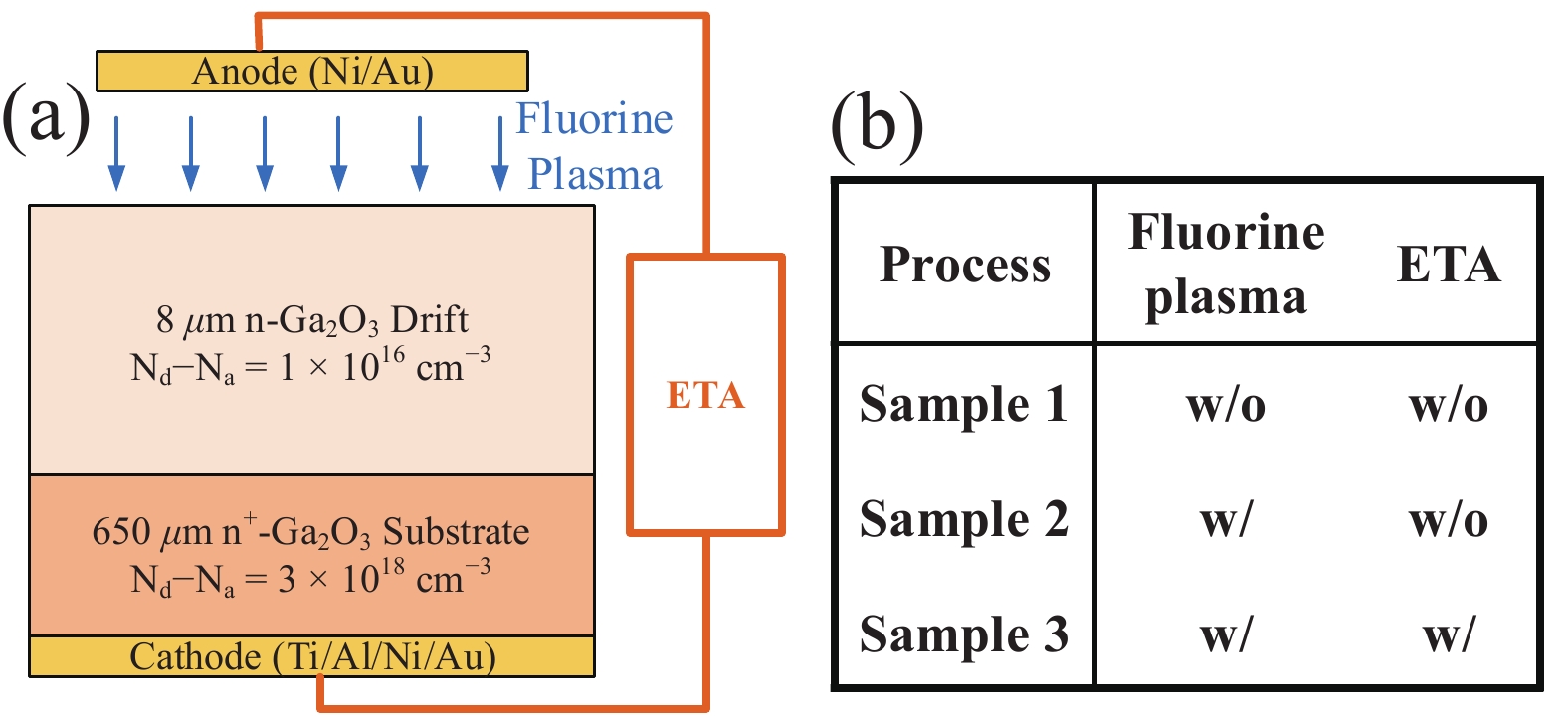
Fig. 1.
(Color online) (a) Schematic cross-section and critical fabrication processes of Ni/β-Ga2O3 SBDs and (b) the process split.
REVIEWS
Jianggen Zhu1, §, Jiaren Feng2, §, Shuting Huang1, Ning Yang1, Binju Qiu1, Enchuan Duan1, Sheng Liu2, Bo Zhang1, Zhaofu Zhang2, 3, 4, and Qi Zhou1, 5, 6,
Corresponding author: Zhaofu Zhang, zhaofuzhang@whu.edu.cn; Qi Zhou, zhouqi@uestc.edu.cn
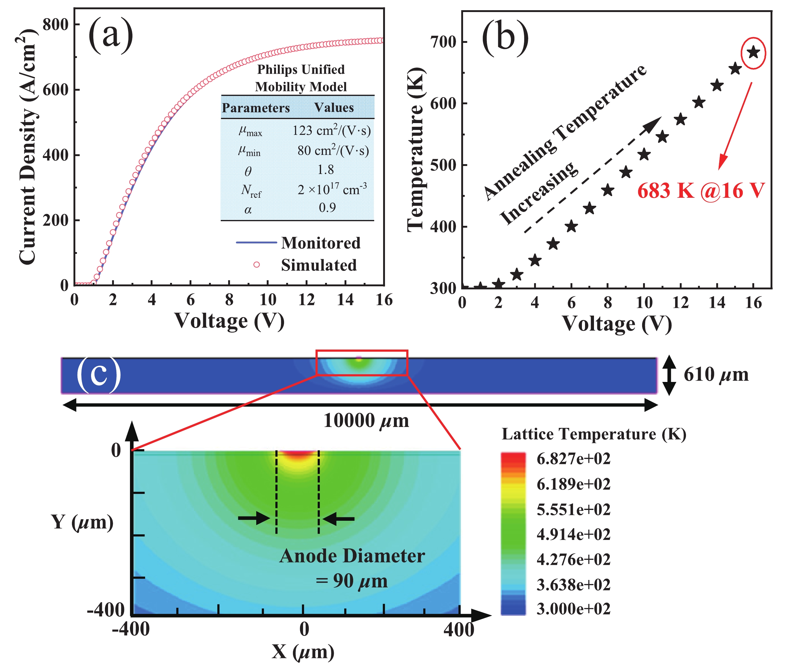
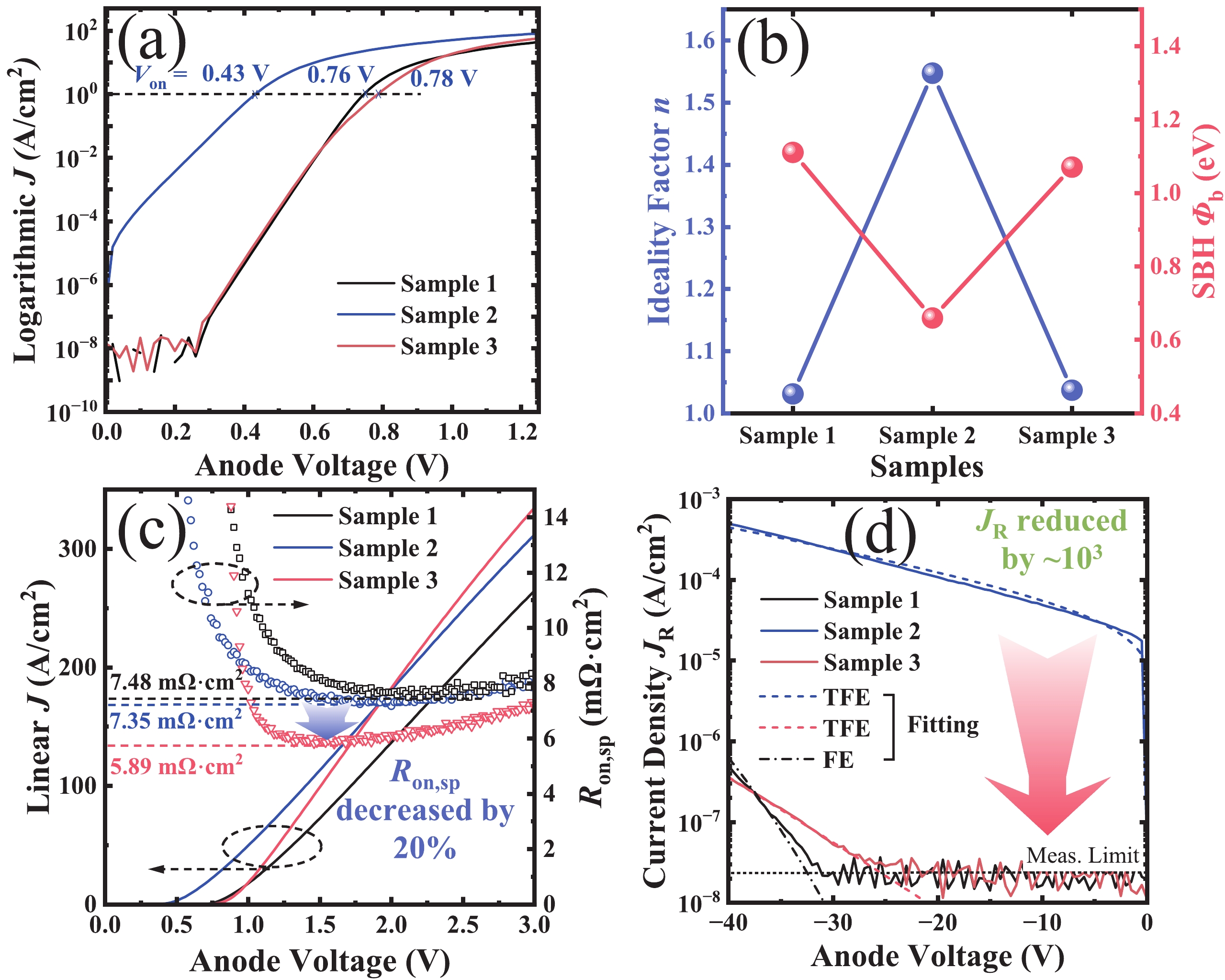
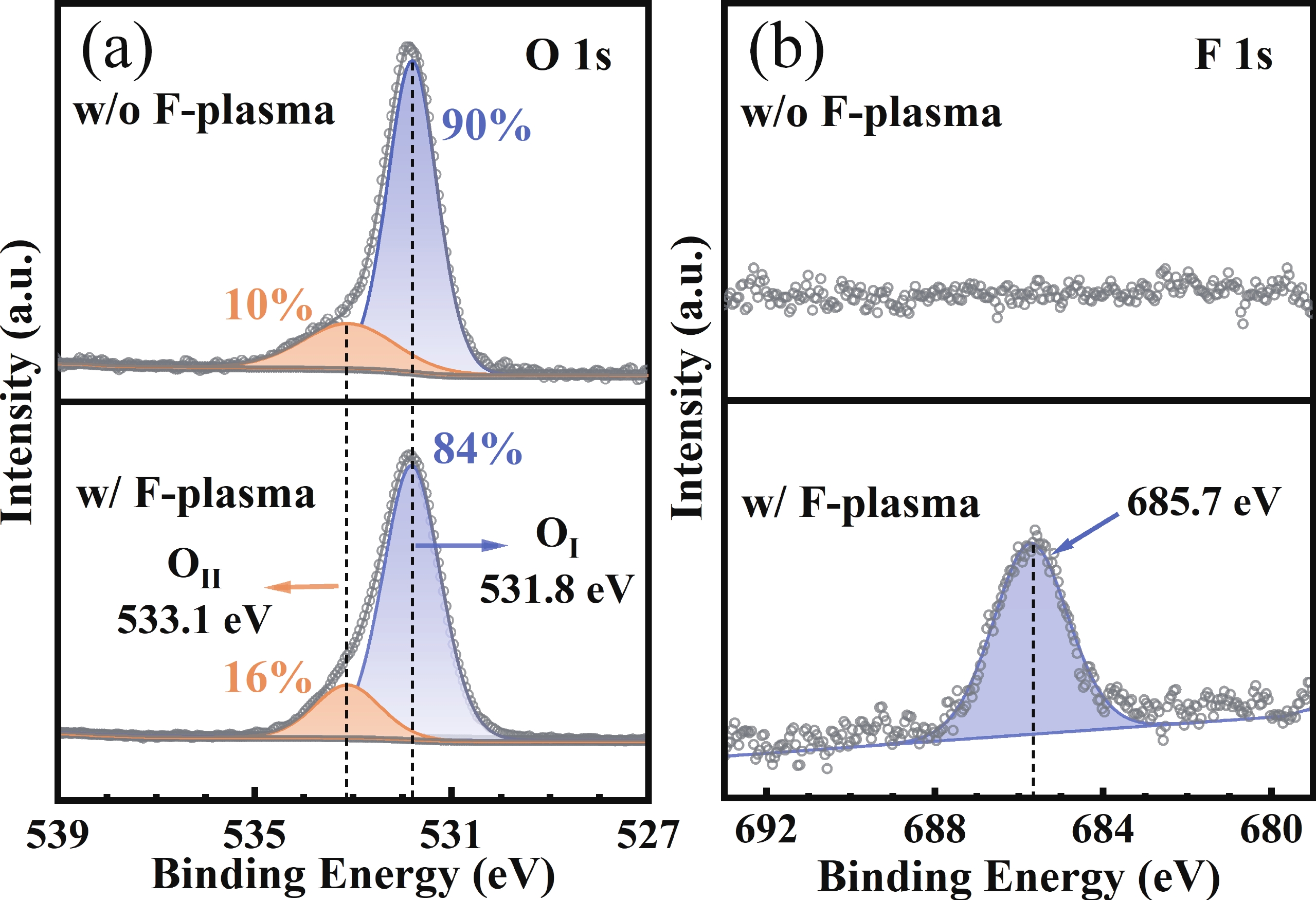
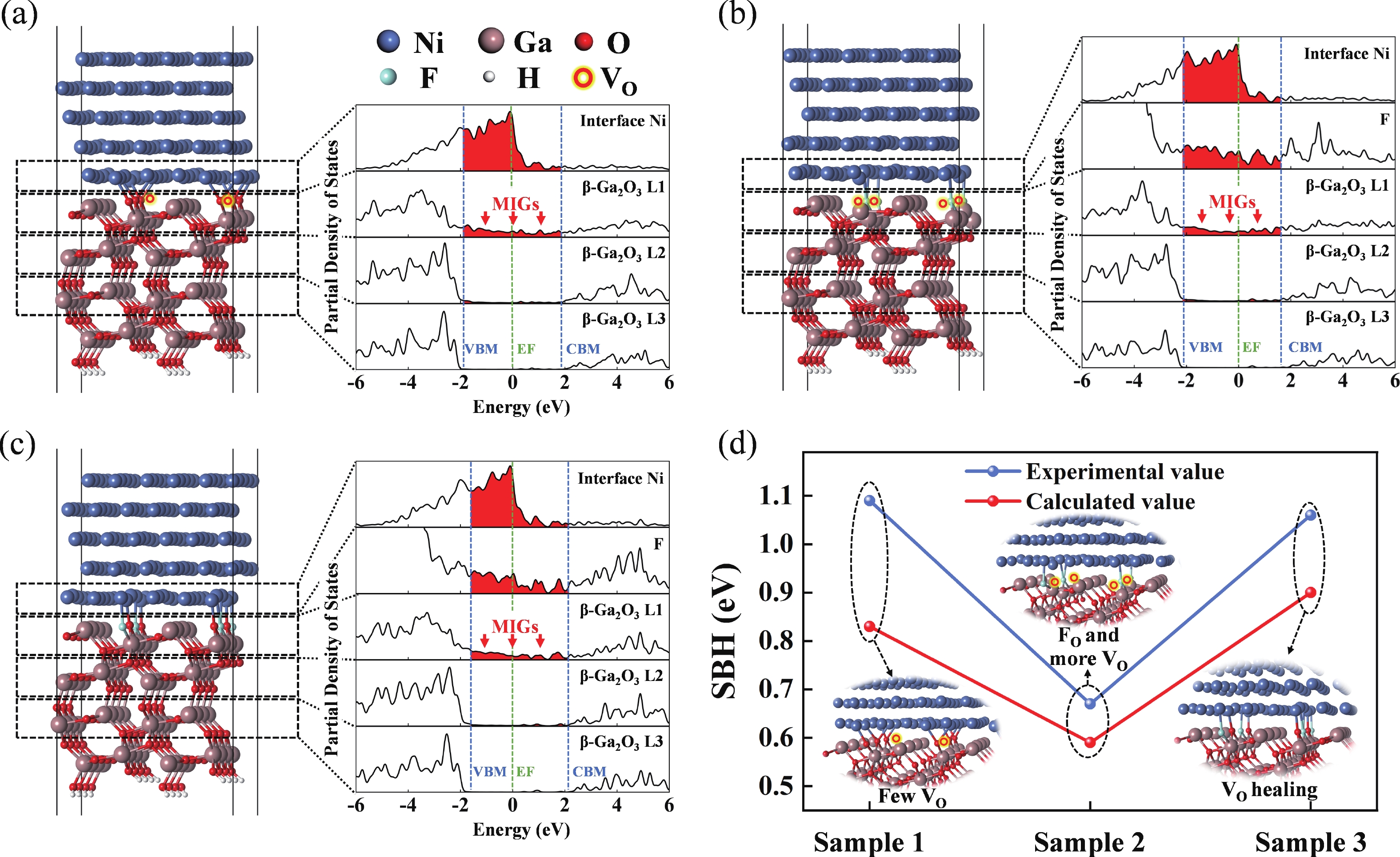
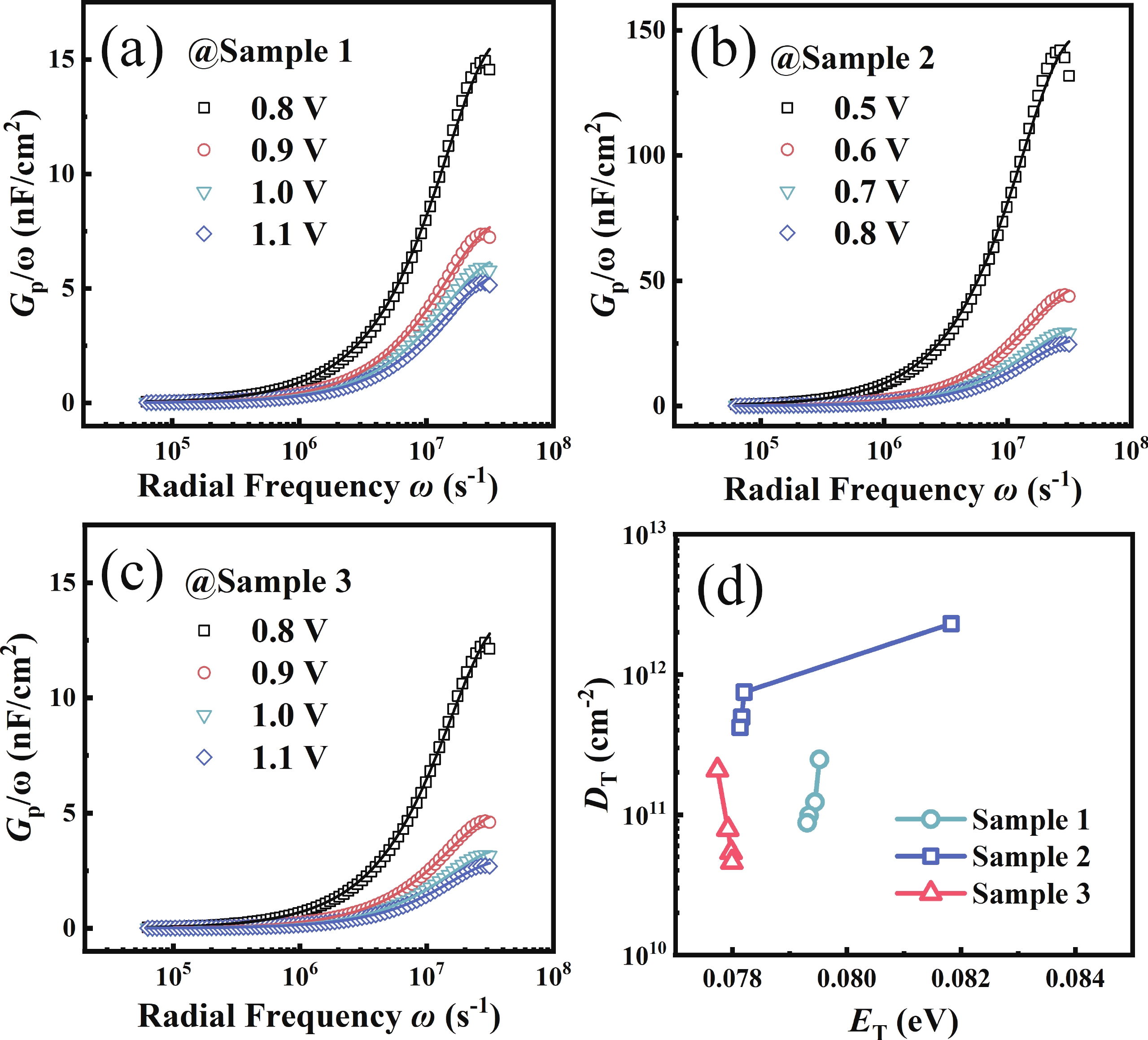
Abstract: The interfacial properties of Schottky contacts crucially affect the performance of power devices. While a few studies have explored the impact of fluorine on Schottky contacts, a comprehensive theoretical explanation supported by experimental evidence remains lacking. This work investigates the effects of fluorine incorporation and electrothermal annealing (ETA) on the current transport process at Ni/β-Ga2O3 Schottky contacts. X-ray photoelectron spectroscopy and first-principles calculations confirm the presence of fluorine substitutions for oxygen and oxygen vacancies and their lowering effect on the Schottky barrier heights. Additionally, accurate electrothermal hybrid TCAD simulations validates the extremely short-duration high temperatures (683 K) induced by ETA, which facilitates lattice rearrangement and reduces interface trap states. The interface trap states are quantitatively resolved through frequency-dependent conductance technique, showing the trap density (DT) reduction from (0.88−2.48) × 1011 cm−2·eV−1 to (0.46−2.09) × 1011 cm−2·eV−1. This investigation offers critical insights into the β-Ga2O3 contacts with the collaborative treatment and solids the promotion of high-performance β-Ga2O3 power devices.
Key words: Ni/β-Ga2O3 interface, first-principles calculations, Schottky contact, fluorine plasma, electrothermal annealing
| [1] |
Pearton S J, Yang J C, Cary P H IV, et al. A review of Ga2O3 materials, processing, and devices. Appl Phys Rev, 2018, 5(1), 011301 doi: 10.1063/1.5006941
|
| [2] |
Yuan Y, Hao W B, Mu W X, et al. Toward emerging gallium oxide semiconductors: A roadmap. Fundam Res, 2021, 1(6), 697 doi: 10.1016/j.fmre.2021.11.002
|
| [3] |
Zhang J Y, Shi J L, Qi D C, et al. Recent progress on the electronic structure, defect, and doping properties of Ga2O3. APL Mater, 2020, 8(2), 020906 doi: 10.1063/1.5142999
|
| [4] |
Kuramata A, Koshi K, Watanabe S, et al. High-quality β-Ga2O3 single crystals grown by edge-defined film-fed growth. Jpn J Appl Phys, 2016, 55(12), 1202A2 doi: 10.7567/JJAP.55.1202A2
|
| [5] |
Murakami H, Nomura K, Goto K, et al. Homoepitaxial growth of β-Ga2O3 layers by halide vapor phase epitaxy. Appl Phys Express, 2015, 8(1), 015503 doi: 10.7567/APEX.8.015503
|
| [6] |
Zhang Z, Yan P R, Song Q W, et al. Recent progress of Ga2O3 materials and devices based on the low-cost, vacuum-free Mist-CVD epitaxial growth method. Fundam Res, 2024, 4(5), 1292 doi: 10.1016/j.fmre.2023.01.001
|
| [7] |
Xiu X Q, Zhang L Y, Li Y W, et al. Application of halide vapor phase epitaxy for the growth of ultra-wide band gap Ga2O3. J Semicond, 2019, 40(1), 011805 doi: 10.1088/1674-4926/40/1/011805
|
| [8] |
Ji X Q, Lu C, Yan Z Y, et al. A review of gallium oxide-based power Schottky barrier diodes. J Phys D: Appl Phys, 2022, 55(44), 443002 doi: 10.1088/1361-6463/ac855c
|
| [9] |
He Q M, Hao W B, Zhou X Z, et al. Over 1 GW/cm2 vertical Ga2O3 Schottky barrier diodes without edge termination. IEEE Electron Device Lett, 2022, 43(2), 264 doi: 10.1109/LED.2021.3133866
|
| [10] |
Yue S Z, Zheng X F, Hong Y H, et al. Effects of neutron irradiation on electrical performance of β-Ga2O3 Schottky barrier diodes. IEEE Trans Electron Devices, 2023, 70(6), 3026 doi: 10.1109/TED.2023.3270124
|
| [11] |
Chen H, Wang H Y, Wang C, et al. Low specific on-resistance and low leakage current β-Ga2O3 (001) Schottky barrier diode through contact pre-treatment. 2022 IEEE 34th International Symposium on Power Semiconductor Devices and ICs (ISPSD), 2022, 145
|
| [12] |
Hong Y H, Zheng X F, He Y L, et al. The optimized interface characteristics of β-Ga2O3 Schottky barrier diode with low temperature annealing. Appl Phys Lett, 2021, 119(13), 132103 doi: 10.1063/5.0063458
|
| [13] |
Roy S, Bhattacharyya A, Peterson C, et al. 2.1 kV (001)-β-Ga2O3 vertical Schottky barrier diode with high-k oxide field plate. Appl Phys Lett, 2023, 122(15), 152101 doi: 10.1063/5.0137935
|
| [14] |
Ji M, Taylor N R, Kravchenko I, et al. Demonstration of large-size vertical Ga2O3 Schottky barrier diodes. IEEE Trans Power Electron, 2021, 36(1), 41 doi: 10.1109/TPEL.2020.3001530
|
| [15] |
Yan Q L, Gong H H, Zhou H, et al. Low density of interface trap states and temperature dependence study of Ga2O3 Schottky barrier diode with p-NiOx termination. Appl Phys Lett, 2022, 120(9), 092106 doi: 10.1063/5.0082377
|
| [16] |
Lin C H, Yuda Y, Wong M H, et al. Vertical Ga2O3 Schottky barrier diodes with guard ring formed by nitrogen-ion implantation. IEEE Electron Device Lett, 2019, 40(9), 1487 doi: 10.1109/LED.2019.2927790
|
| [17] |
Sun J B, Chen Z Y, Zhou S Q, et al. Vertical sidewall of silicon nitride mask and smooth surface of etched-silicon simultaneously obtained using CHF3/O2 inductively coupled plasma. Vacuum, 2023, 207, 111650 doi: 10.1016/j.vacuum.2022.111650
|
| [18] |
Schaepkens M, Oehrlein G S. A review of SiO2 etching studies in inductively coupled fluorocarbon plasmas. J Electrochem Soc, 2001, 148(3), C211 doi: 10.1149/1.1348260
|
| [19] |
Fei W X, Bi T, Iwataki M, et al. Oxidized Si terminated diamond and its MOSFET operation with SiO2 gate insulator. Appl Phys Lett, 2020, 116(21), 212103 doi: 10.1063/1.5143982
|
| [20] |
Saito W, Takada Y, Kuraguchi M, et al. Design and demonstration of high breakdown voltage GaN high electron mobility transistor (HEMT) using field plate structure for power electronics applications. Jpn J Appl Phys, 2004, 43(4S), 2239 doi: 10.1143/JJAP.43.2239
|
| [21] |
Yang J C, Fares C, Ren F, et al. Effects of fluorine incorporation into β-Ga2O3. J Appl Phys, 2018, 123(16), 165706 doi: 10.1063/1.5031001
|
| [22] |
Yang J C, Sparks Z, Ren F, et al. Effect of surface treatments on electrical properties of β-Ga2O3. J Vac Sci Technol B, 2018, 36(6), 061201 doi: 10.1116/1.5052229
|
| [23] |
Kim C K, Kim E, Lee M K, et al. Electrothermal annealing (ETA) method to enhance the electrical performance of amorphous-oxide-semiconductor (AOS) thin-film transistors (TFTs). ACS Appl Mater Interfaces, 2016, 8(36), 23820 doi: 10.1021/acsami.6b06377
|
| [24] |
Bae H, Lee K S, Ye P D, et al. Current annealing to improve drain output performance of β-Ga2O3 field-effect transistor. Solid State Electron, 2021, 185, 108134 doi: 10.1016/j.sse.2021.108134
|
| [25] |
Wong H Y, Fossito Tenkeu A C. Advanced TCAD simulation and calibration of gallium oxide vertical transistor. J Solid State Sci Technol, 2020, 9(3), 035003 doi: 10.1149/2162-8777/ab7673
|
| [26] |
Santia M D, Tandon N, Albrecht J D. Lattice thermal conductivity in β-Ga2O3 from first principles. Appl Phys Lett, 2015, 107(4), 041907 doi: 10.1063/1.4927742
|
| [27] |
Oktapia D, Nurfani E, Wahjoedi B A, et al. Seedless hydrothermal growth of hexagonal prism ZnO for photocatalytic degradation of methylene blue: The effect of pH and post-annealing treatment. Semicond Sci Technol, 2023, 38(10), 105005 doi: 10.1088/1361-6641/acf397
|
| [28] |
Kresse G, Furthmüller J. Efficient iterative schemes for ab initio total-energy calculations using a plane-wave basis set. Phys Rev B Condens Matter, 1996, 54(16), 11169 doi: 10.1103/PhysRevB.54.11169
|
| [29] |
Perdew J P, Burke K, Ernzerhof M. Generalized gradient approximation made simple. Phys Rev Lett, 1996, 77(18), 3865 doi: 10.1103/PhysRevLett.77.3865
|
| [30] |
Li W S, Saraswat D, Long Y Y, et al. Near-ideal reverse leakage current and practical maximum electric field in β-Ga2O3 Schottky barrier diodes. Appl Phys Lett, 2020, 116(19), 192101 doi: 10.1063/5.0007715
|
| [31] |
Sasaki K, Higashiwaki M, Kuramata A, et al. Ga2O3 Schottky barrier diodes fabricated by using single-crystal β-Ga2O3 (010) substrates. IEEE Electron Device Lett, 2013, 34(4), 493 doi: 10.1109/LED.2013.2244057
|
| [32] |
Wang Z P, Gong H H, Yu X X, et al. Traps inhomogeneity induced conversion of Shockley–Read–Hall recombination in NiO/β-Ga2O3 p+–n heterojunction diodes. Appl Phys Lett, 2023, 122(15), 152102 doi: 10.1063/5.0138426
|
| [33] |
Liu J J, Yan J L, Shi L, et al. Electrical and optical properties of deep ultraviolet transparent conductive Ga2O3/ITO films by magnetron sputtering. J Semicond, 2010, 31(10), 103001 doi: 10.1088/1674-4926/31/10/103001
|
| [34] |
Yang J C, Ren F, Khanna R, et al. Annealing of dry etch damage in metallized and bare (-201) Ga2O3. J Vac Sci Technol B, 2017, 35(5), 051201 doi: 10.1116/1.4986300
|
| [35] |
Jeong Y J, Yang J Y, Lee C H, et al. Fluorine-based plasma treatment for hetero-epitaxial β-Ga2O3 MOSFETs. Appl Surf Sci, 2021, 558, 149936 doi: 10.1016/j.apsusc.2021.149936
|
| [36] |
Morimoto S, Nishinaka H, Yoshimoto M. Growth and characterization of F-doped α-Ga2O3 thin films with low electrical resistivity. Thin Solid Films, 2019, 682, 18 doi: 10.1016/j.tsf.2019.04.051
|
| [37] |
Varley J B, Weber J R, Janotti A, et al. Oxygen vacancies and donor impurities in β-Ga2O3. Appl Phys Lett, 2010, 97(14), 142106 doi: 10.1063/1.3499306
|
| [38] |
Sze S M, Ng K K. Physics of Semiconductor Devices. Wiley, 2006
|
| [39] |
Sdoeung S, Sasaki K, Kawasaki K, et al. Polycrystalline defects: Origin of leakage current: In halide vapor phase epitaxial (001) β-Ga2O3 Schottky barrier diodes identified via ultrahigh sensitive emission microscopy and synchrotron X-ray topography. Appl Phys Express, 2021, 14(3), 036502 doi: 10.35848/1882-0786/abde74
|
| [40] |
Rafique S, Han L, Zhao H P. Thermal annealing effect on β-Ga2O3 thin film solar blind photodetector heteroepitaxially grown on sapphire substrate. Phys Status Solidi A, 2017, 214(8), 1700063 doi: 10.1002/pssa.201700063
|
| [41] |
Guo D Y, Wu Z P, An Y H, et al. Oxygen vacancy tuned Ohmic-Schottky conversion for enhanced performance in β-Ga2O3 solar-blind ultraviolet photodetectors. Appl Phys Lett, 2014, 105(2), 023507 doi: 10.1063/1.4890524
|
| [42] |
Liu B, Gu M, Liu X L, et al. First-principles study of fluorine-doped zinc oxide. Appl Phys Lett, 2010, 97(12), 122101 doi: 10.1063/1.3492444
|
| [43] |
Zhang Z F, Qian Q K, Li B K, et al. Interface engineering of monolayer MoS2/GaN hybrid heterostructure: Modified band alignment for photocatalytic water splitting application by nitridation treatment. ACS Appl Mater Interfaces, 2018, 10(20), 17419 doi: 10.1021/acsami.8b01286
|
| [44] |
Yu W, Feng J R, Gui Q Z, et al. Metal contacts and Schottky barriers at β-Ga2O3 interfaces: High-throughput-assisted first-principles calculations. J Appl Phys, 2025, 137(11), 115701 doi: 10.1063/5.0256577
|
| [45] |
Robertson J. Band offsets, Schottky barrier heights, and their effects on electronic devices. J Vac Sci Technol A Vac Surf Films, 2013, 31(5), 050821 doi: 10.1116/1.4818426
|
| [46] |
He Y L, Sheng B S, Hong Y H, et al. Research on the β-Ga2O3 Schottky barrier diodes with oxygen-containing plasma treatment. Appl Phys Lett, 2023, 122(16), 163503 doi: 10.1063/5.0145659
|
| [47] |
Schroder D K. Semiconductor Material and Device Characterization. Wiley, 2005
|


Article views: 19 Times PDF downloads: 4 Times Cited by: 0 Times
Received: 21 May 2025 Revised: 18 August 2025 Online: Accepted Manuscript: 03 September 2025
| Citation: |
Jianggen Zhu, Jiaren Feng, Shuting Huang, Ning Yang, Binju Qiu, Enchuan Duan, Sheng Liu, Bo Zhang, Zhaofu Zhang, Qi Zhou. Impact of Fluorine Plasma and Electrothermal Annealing on the Interfacial Properties at Ni/β-Ga2O3 Schottky Contacts[J]. Journal of Semiconductors, 2025, In Press. doi: 10.1088/1674-4926/25020020
****
J G Zhu, J R Feng, S T Huang, N Yang, B J Qiu, E C Duan, S Liu, B Zhang, Z F Zhang, and Q Zhou, Impact of Fluorine Plasma and Electrothermal Annealing on the Interfacial Properties at Ni/β-Ga2O3 Schottky Contacts[J]. J. Semicond., 2025, accepted doi: 10.1088/1674-4926/25020020

|
 Jianggen Zhu received the B.S. degree in microelectronics science and engineering from Central South University in 2022. Currently, he is working toward the Ph.D. degree in electronic science and technology from University of Electronic Science and Technology of China. His research focuses on manufacturing process and reliability of wide bandgap power devices
 Jiaren Feng received his bachelor's degree in the school of microelectronics in Wuhan University, Wuhan, China, in 2023. Currently, he is working toward the Ph.D. degree in the school of integrated circuits in Wuhan University. He now focuses on the surface and interface science of wide bandgap semiconductors
 Zhaofu Zhang is currently a Professor at Wuhan University. He worked as Research Associate at University of Cambridge (2019-2022), after he received the Ph.D. degree from Hong Kong University of Science and Technology in 2018. He focuses on surface, interface, and defects in wide bandgap semiconductors, and the rational design of semiconductor devices
 Qi Zhou received his Ph.D. degree in electronic and computer engineering from the Hong Kong University of Science and Technology, Hong Kong, in 2012. He is currently a professor with the University of Electronic Science and Technology of China, Chengdu, China. His research interests include GaN power devices and integrated circuits and applications
| [1] |
Pearton S J, Yang J C, Cary P H IV, et al. A review of Ga2O3 materials, processing, and devices. Appl Phys Rev, 2018, 5(1), 011301 doi: 10.1063/1.5006941
|
| [2] |
Yuan Y, Hao W B, Mu W X, et al. Toward emerging gallium oxide semiconductors: A roadmap. Fundam Res, 2021, 1(6), 697 doi: 10.1016/j.fmre.2021.11.002
|
| [3] |
Zhang J Y, Shi J L, Qi D C, et al. Recent progress on the electronic structure, defect, and doping properties of Ga2O3. APL Mater, 2020, 8(2), 020906 doi: 10.1063/1.5142999
|
| [4] |
Kuramata A, Koshi K, Watanabe S, et al. High-quality β-Ga2O3 single crystals grown by edge-defined film-fed growth. Jpn J Appl Phys, 2016, 55(12), 1202A2 doi: 10.7567/JJAP.55.1202A2
|
| [5] |
Murakami H, Nomura K, Goto K, et al. Homoepitaxial growth of β-Ga2O3 layers by halide vapor phase epitaxy. Appl Phys Express, 2015, 8(1), 015503 doi: 10.7567/APEX.8.015503
|
| [6] |
Zhang Z, Yan P R, Song Q W, et al. Recent progress of Ga2O3 materials and devices based on the low-cost, vacuum-free Mist-CVD epitaxial growth method. Fundam Res, 2024, 4(5), 1292 doi: 10.1016/j.fmre.2023.01.001
|
| [7] |
Xiu X Q, Zhang L Y, Li Y W, et al. Application of halide vapor phase epitaxy for the growth of ultra-wide band gap Ga2O3. J Semicond, 2019, 40(1), 011805 doi: 10.1088/1674-4926/40/1/011805
|
| [8] |
Ji X Q, Lu C, Yan Z Y, et al. A review of gallium oxide-based power Schottky barrier diodes. J Phys D: Appl Phys, 2022, 55(44), 443002 doi: 10.1088/1361-6463/ac855c
|
| [9] |
He Q M, Hao W B, Zhou X Z, et al. Over 1 GW/cm2 vertical Ga2O3 Schottky barrier diodes without edge termination. IEEE Electron Device Lett, 2022, 43(2), 264 doi: 10.1109/LED.2021.3133866
|
| [10] |
Yue S Z, Zheng X F, Hong Y H, et al. Effects of neutron irradiation on electrical performance of β-Ga2O3 Schottky barrier diodes. IEEE Trans Electron Devices, 2023, 70(6), 3026 doi: 10.1109/TED.2023.3270124
|
| [11] |
Chen H, Wang H Y, Wang C, et al. Low specific on-resistance and low leakage current β-Ga2O3 (001) Schottky barrier diode through contact pre-treatment. 2022 IEEE 34th International Symposium on Power Semiconductor Devices and ICs (ISPSD), 2022, 145
|
| [12] |
Hong Y H, Zheng X F, He Y L, et al. The optimized interface characteristics of β-Ga2O3 Schottky barrier diode with low temperature annealing. Appl Phys Lett, 2021, 119(13), 132103 doi: 10.1063/5.0063458
|
| [13] |
Roy S, Bhattacharyya A, Peterson C, et al. 2.1 kV (001)-β-Ga2O3 vertical Schottky barrier diode with high-k oxide field plate. Appl Phys Lett, 2023, 122(15), 152101 doi: 10.1063/5.0137935
|
| [14] |
Ji M, Taylor N R, Kravchenko I, et al. Demonstration of large-size vertical Ga2O3 Schottky barrier diodes. IEEE Trans Power Electron, 2021, 36(1), 41 doi: 10.1109/TPEL.2020.3001530
|
| [15] |
Yan Q L, Gong H H, Zhou H, et al. Low density of interface trap states and temperature dependence study of Ga2O3 Schottky barrier diode with p-NiOx termination. Appl Phys Lett, 2022, 120(9), 092106 doi: 10.1063/5.0082377
|
| [16] |
Lin C H, Yuda Y, Wong M H, et al. Vertical Ga2O3 Schottky barrier diodes with guard ring formed by nitrogen-ion implantation. IEEE Electron Device Lett, 2019, 40(9), 1487 doi: 10.1109/LED.2019.2927790
|
| [17] |
Sun J B, Chen Z Y, Zhou S Q, et al. Vertical sidewall of silicon nitride mask and smooth surface of etched-silicon simultaneously obtained using CHF3/O2 inductively coupled plasma. Vacuum, 2023, 207, 111650 doi: 10.1016/j.vacuum.2022.111650
|
| [18] |
Schaepkens M, Oehrlein G S. A review of SiO2 etching studies in inductively coupled fluorocarbon plasmas. J Electrochem Soc, 2001, 148(3), C211 doi: 10.1149/1.1348260
|
| [19] |
Fei W X, Bi T, Iwataki M, et al. Oxidized Si terminated diamond and its MOSFET operation with SiO2 gate insulator. Appl Phys Lett, 2020, 116(21), 212103 doi: 10.1063/1.5143982
|
| [20] |
Saito W, Takada Y, Kuraguchi M, et al. Design and demonstration of high breakdown voltage GaN high electron mobility transistor (HEMT) using field plate structure for power electronics applications. Jpn J Appl Phys, 2004, 43(4S), 2239 doi: 10.1143/JJAP.43.2239
|
| [21] |
Yang J C, Fares C, Ren F, et al. Effects of fluorine incorporation into β-Ga2O3. J Appl Phys, 2018, 123(16), 165706 doi: 10.1063/1.5031001
|
| [22] |
Yang J C, Sparks Z, Ren F, et al. Effect of surface treatments on electrical properties of β-Ga2O3. J Vac Sci Technol B, 2018, 36(6), 061201 doi: 10.1116/1.5052229
|
| [23] |
Kim C K, Kim E, Lee M K, et al. Electrothermal annealing (ETA) method to enhance the electrical performance of amorphous-oxide-semiconductor (AOS) thin-film transistors (TFTs). ACS Appl Mater Interfaces, 2016, 8(36), 23820 doi: 10.1021/acsami.6b06377
|
| [24] |
Bae H, Lee K S, Ye P D, et al. Current annealing to improve drain output performance of β-Ga2O3 field-effect transistor. Solid State Electron, 2021, 185, 108134 doi: 10.1016/j.sse.2021.108134
|
| [25] |
Wong H Y, Fossito Tenkeu A C. Advanced TCAD simulation and calibration of gallium oxide vertical transistor. J Solid State Sci Technol, 2020, 9(3), 035003 doi: 10.1149/2162-8777/ab7673
|
| [26] |
Santia M D, Tandon N, Albrecht J D. Lattice thermal conductivity in β-Ga2O3 from first principles. Appl Phys Lett, 2015, 107(4), 041907 doi: 10.1063/1.4927742
|
| [27] |
Oktapia D, Nurfani E, Wahjoedi B A, et al. Seedless hydrothermal growth of hexagonal prism ZnO for photocatalytic degradation of methylene blue: The effect of pH and post-annealing treatment. Semicond Sci Technol, 2023, 38(10), 105005 doi: 10.1088/1361-6641/acf397
|
| [28] |
Kresse G, Furthmüller J. Efficient iterative schemes for ab initio total-energy calculations using a plane-wave basis set. Phys Rev B Condens Matter, 1996, 54(16), 11169 doi: 10.1103/PhysRevB.54.11169
|
| [29] |
Perdew J P, Burke K, Ernzerhof M. Generalized gradient approximation made simple. Phys Rev Lett, 1996, 77(18), 3865 doi: 10.1103/PhysRevLett.77.3865
|
| [30] |
Li W S, Saraswat D, Long Y Y, et al. Near-ideal reverse leakage current and practical maximum electric field in β-Ga2O3 Schottky barrier diodes. Appl Phys Lett, 2020, 116(19), 192101 doi: 10.1063/5.0007715
|
| [31] |
Sasaki K, Higashiwaki M, Kuramata A, et al. Ga2O3 Schottky barrier diodes fabricated by using single-crystal β-Ga2O3 (010) substrates. IEEE Electron Device Lett, 2013, 34(4), 493 doi: 10.1109/LED.2013.2244057
|
| [32] |
Wang Z P, Gong H H, Yu X X, et al. Traps inhomogeneity induced conversion of Shockley–Read–Hall recombination in NiO/β-Ga2O3 p+–n heterojunction diodes. Appl Phys Lett, 2023, 122(15), 152102 doi: 10.1063/5.0138426
|
| [33] |
Liu J J, Yan J L, Shi L, et al. Electrical and optical properties of deep ultraviolet transparent conductive Ga2O3/ITO films by magnetron sputtering. J Semicond, 2010, 31(10), 103001 doi: 10.1088/1674-4926/31/10/103001
|
| [34] |
Yang J C, Ren F, Khanna R, et al. Annealing of dry etch damage in metallized and bare (-201) Ga2O3. J Vac Sci Technol B, 2017, 35(5), 051201 doi: 10.1116/1.4986300
|
| [35] |
Jeong Y J, Yang J Y, Lee C H, et al. Fluorine-based plasma treatment for hetero-epitaxial β-Ga2O3 MOSFETs. Appl Surf Sci, 2021, 558, 149936 doi: 10.1016/j.apsusc.2021.149936
|
| [36] |
Morimoto S, Nishinaka H, Yoshimoto M. Growth and characterization of F-doped α-Ga2O3 thin films with low electrical resistivity. Thin Solid Films, 2019, 682, 18 doi: 10.1016/j.tsf.2019.04.051
|
| [37] |
Varley J B, Weber J R, Janotti A, et al. Oxygen vacancies and donor impurities in β-Ga2O3. Appl Phys Lett, 2010, 97(14), 142106 doi: 10.1063/1.3499306
|
| [38] |
Sze S M, Ng K K. Physics of Semiconductor Devices. Wiley, 2006
|
| [39] |
Sdoeung S, Sasaki K, Kawasaki K, et al. Polycrystalline defects: Origin of leakage current: In halide vapor phase epitaxial (001) β-Ga2O3 Schottky barrier diodes identified via ultrahigh sensitive emission microscopy and synchrotron X-ray topography. Appl Phys Express, 2021, 14(3), 036502 doi: 10.35848/1882-0786/abde74
|
| [40] |
Rafique S, Han L, Zhao H P. Thermal annealing effect on β-Ga2O3 thin film solar blind photodetector heteroepitaxially grown on sapphire substrate. Phys Status Solidi A, 2017, 214(8), 1700063 doi: 10.1002/pssa.201700063
|
| [41] |
Guo D Y, Wu Z P, An Y H, et al. Oxygen vacancy tuned Ohmic-Schottky conversion for enhanced performance in β-Ga2O3 solar-blind ultraviolet photodetectors. Appl Phys Lett, 2014, 105(2), 023507 doi: 10.1063/1.4890524
|
| [42] |
Liu B, Gu M, Liu X L, et al. First-principles study of fluorine-doped zinc oxide. Appl Phys Lett, 2010, 97(12), 122101 doi: 10.1063/1.3492444
|
| [43] |
Zhang Z F, Qian Q K, Li B K, et al. Interface engineering of monolayer MoS2/GaN hybrid heterostructure: Modified band alignment for photocatalytic water splitting application by nitridation treatment. ACS Appl Mater Interfaces, 2018, 10(20), 17419 doi: 10.1021/acsami.8b01286
|
| [44] |
Yu W, Feng J R, Gui Q Z, et al. Metal contacts and Schottky barriers at β-Ga2O3 interfaces: High-throughput-assisted first-principles calculations. J Appl Phys, 2025, 137(11), 115701 doi: 10.1063/5.0256577
|
| [45] |
Robertson J. Band offsets, Schottky barrier heights, and their effects on electronic devices. J Vac Sci Technol A Vac Surf Films, 2013, 31(5), 050821 doi: 10.1116/1.4818426
|
| [46] |
He Y L, Sheng B S, Hong Y H, et al. Research on the β-Ga2O3 Schottky barrier diodes with oxygen-containing plasma treatment. Appl Phys Lett, 2023, 122(16), 163503 doi: 10.1063/5.0145659
|
| [47] |
Schroder D K. Semiconductor Material and Device Characterization. Wiley, 2005
|
 Supplementary_materials.pdf
|

|

 WeChat ID
Journal of Semiconductors © 2017 All Rights Reserved 京ICP备05085259号-2

 DownLoad:

