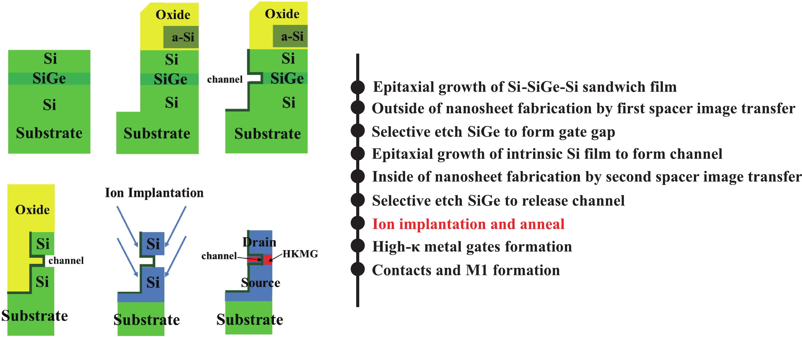
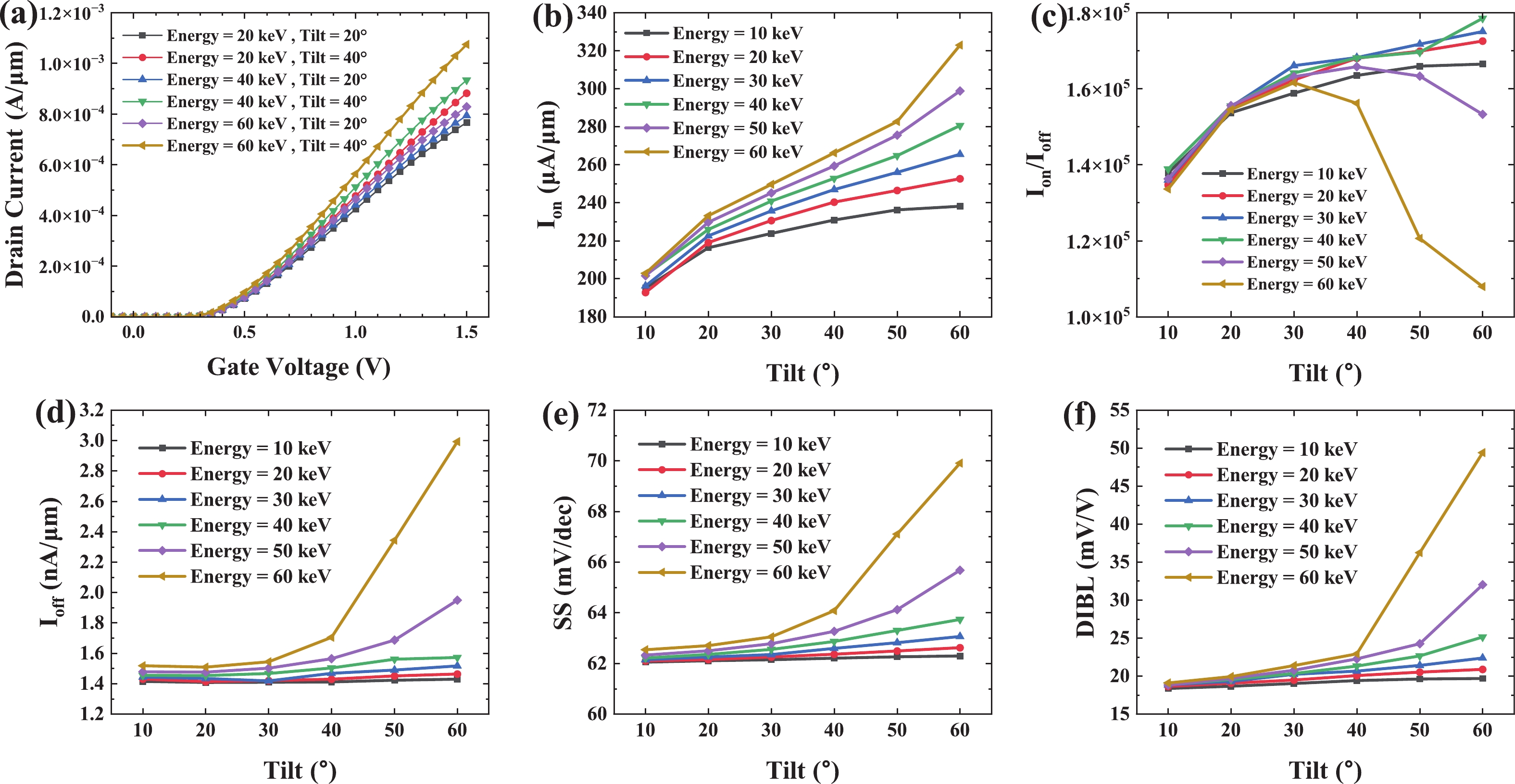
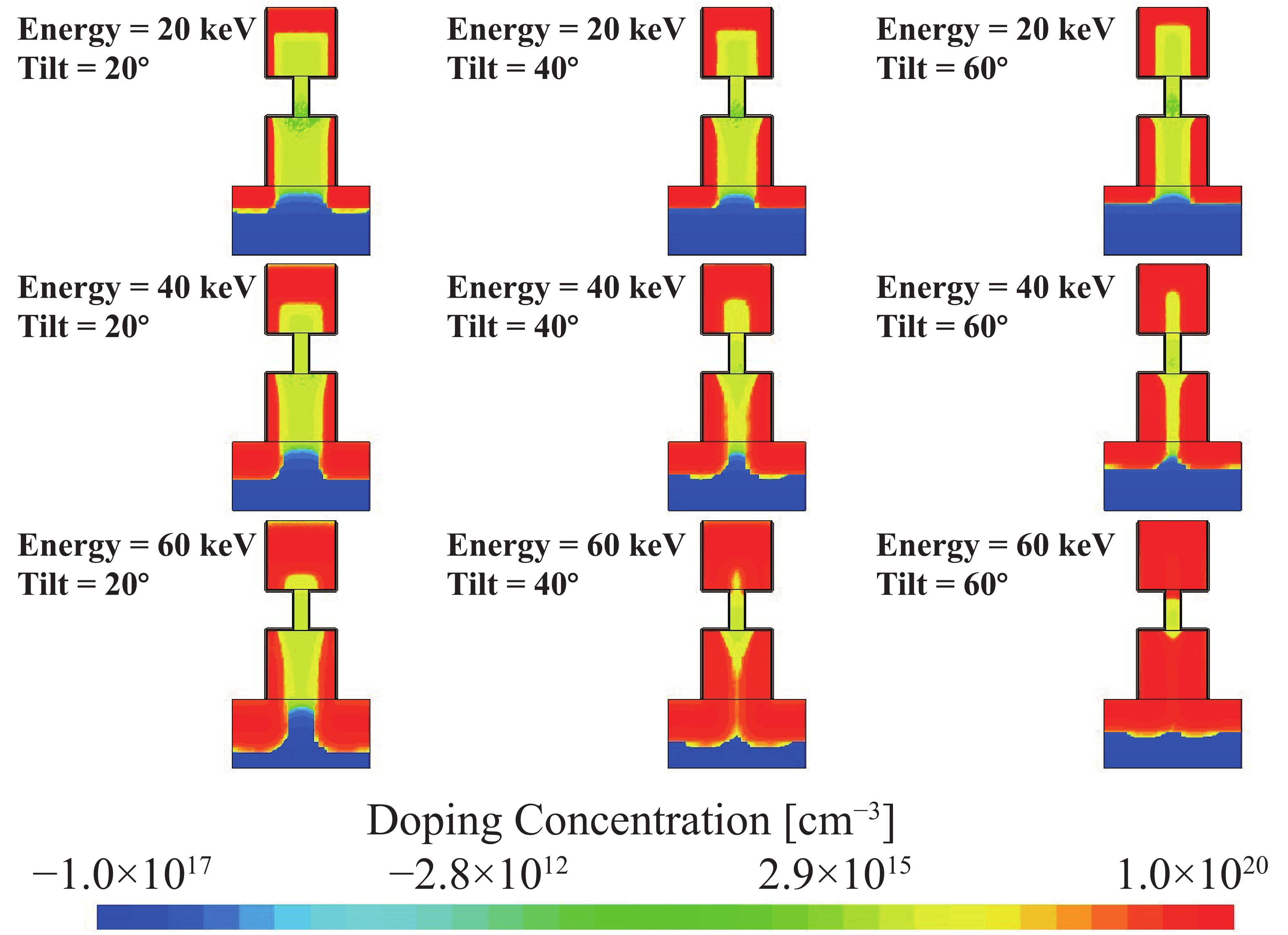
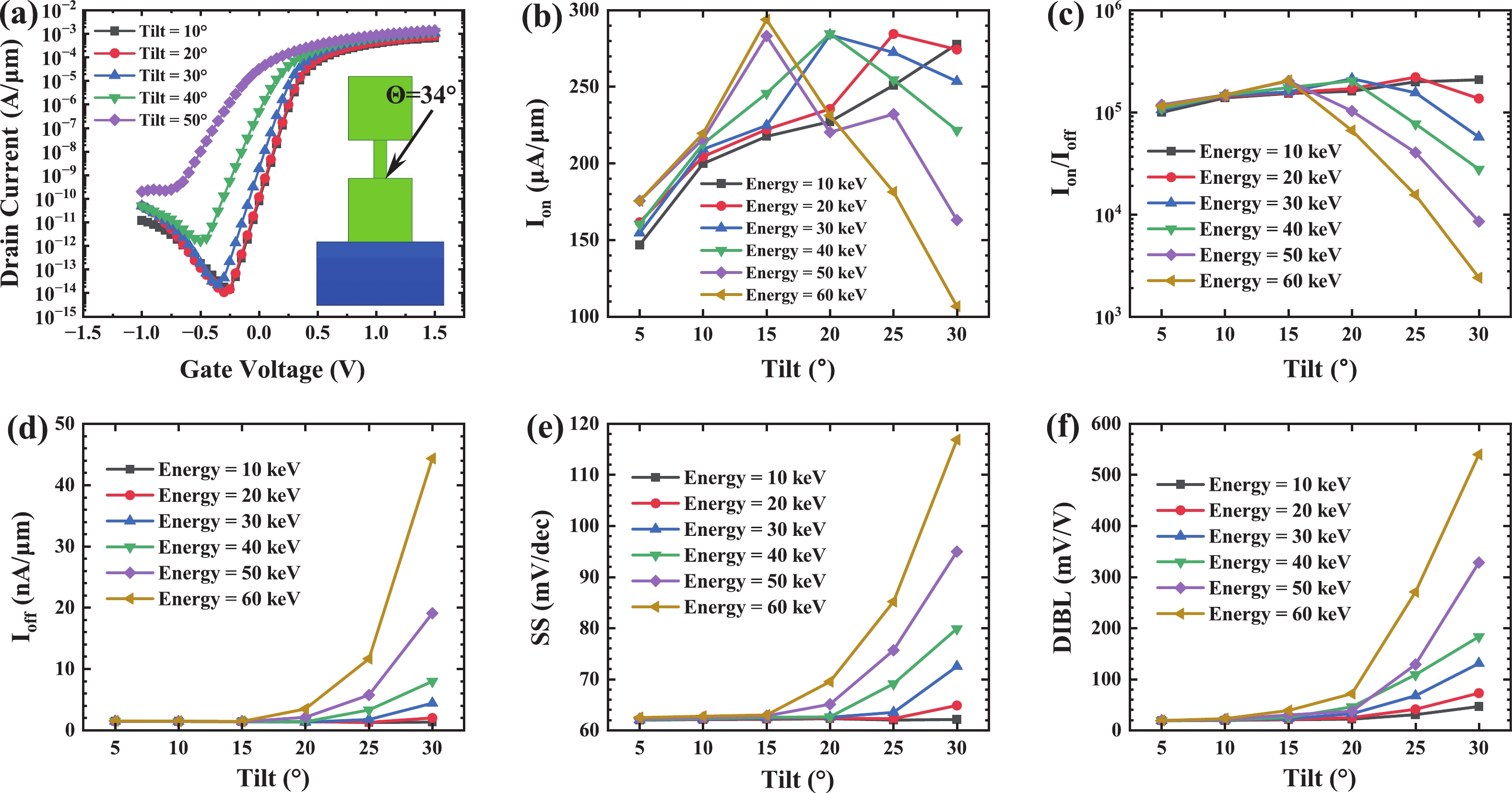
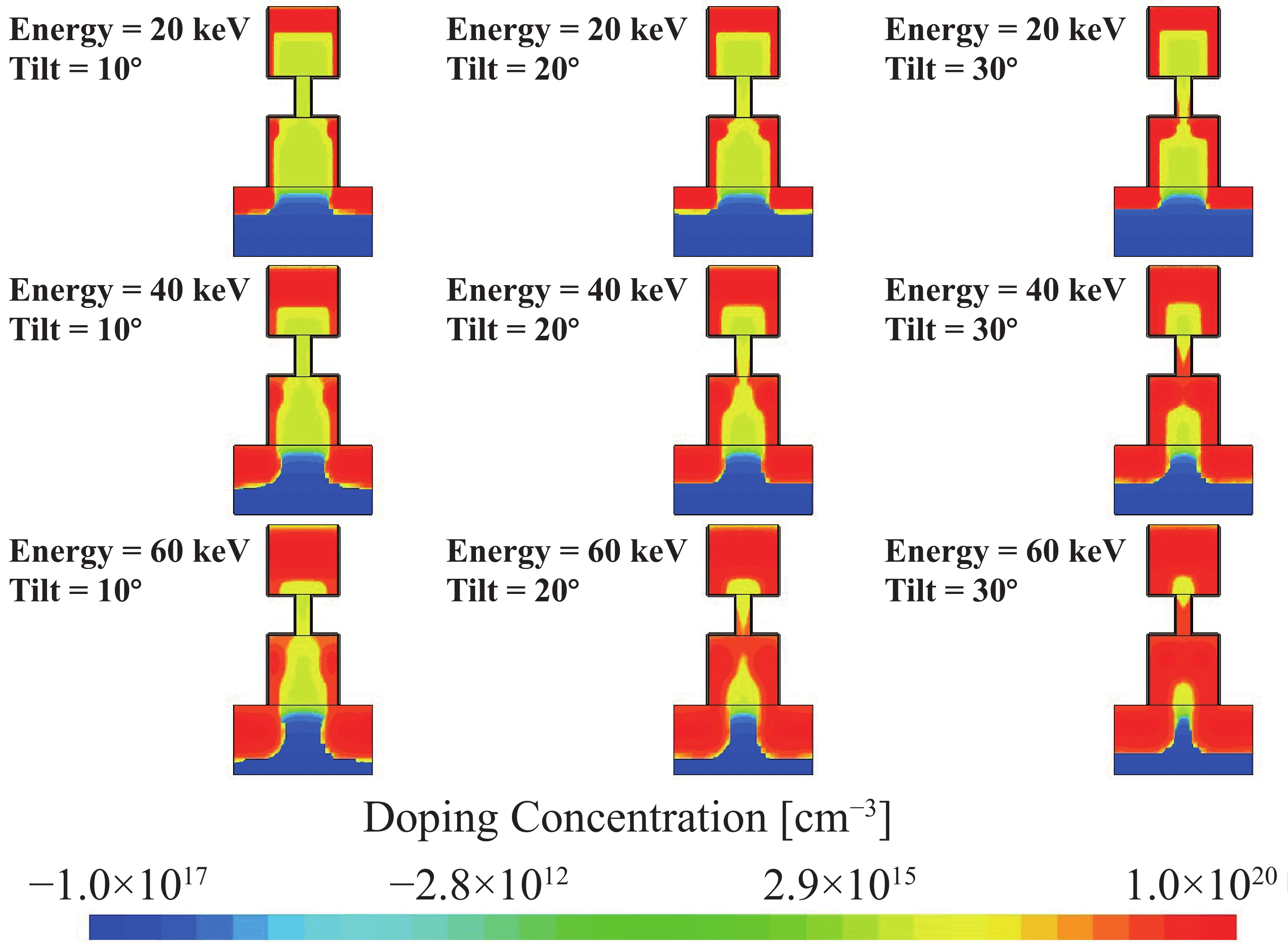
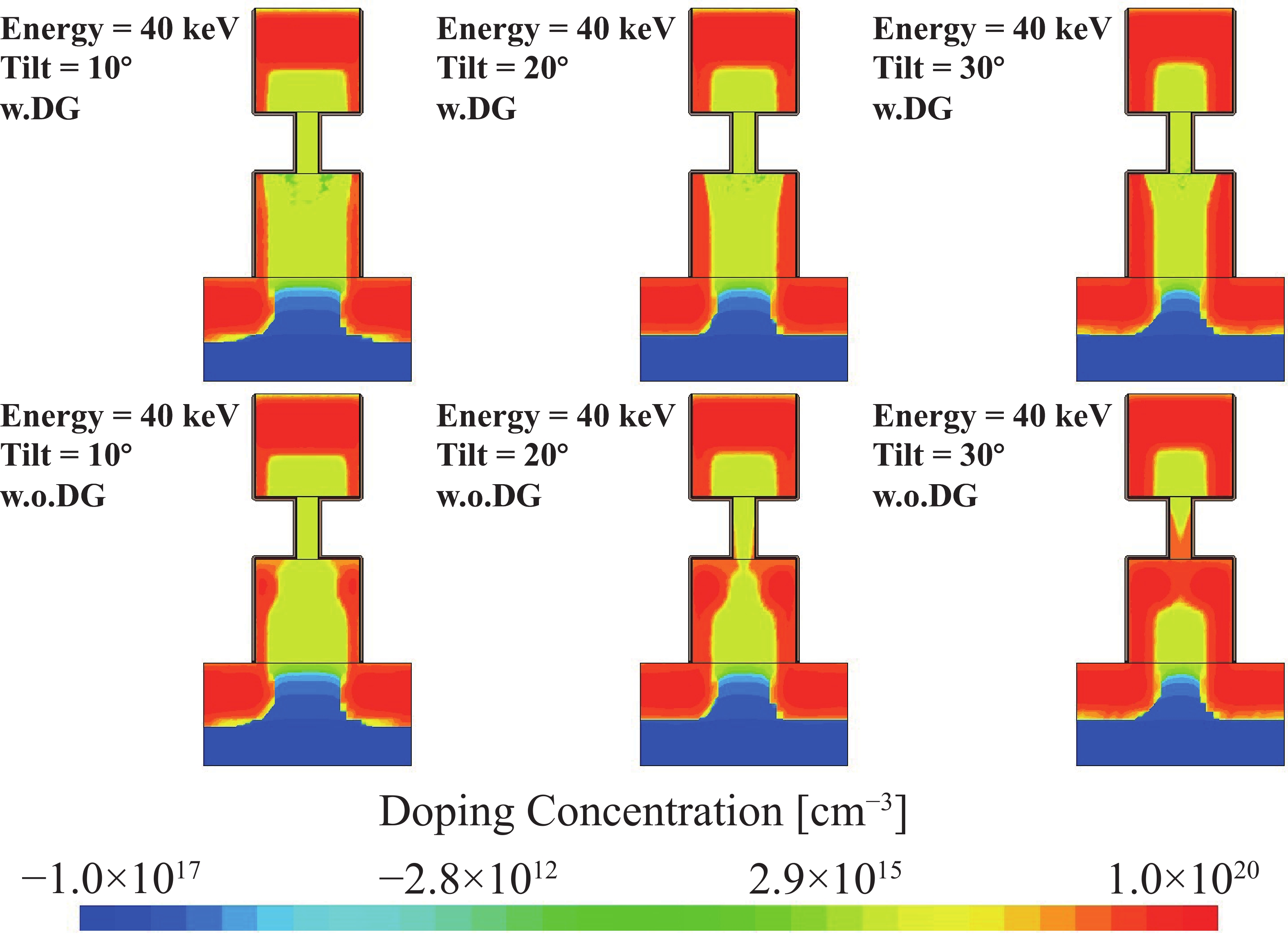
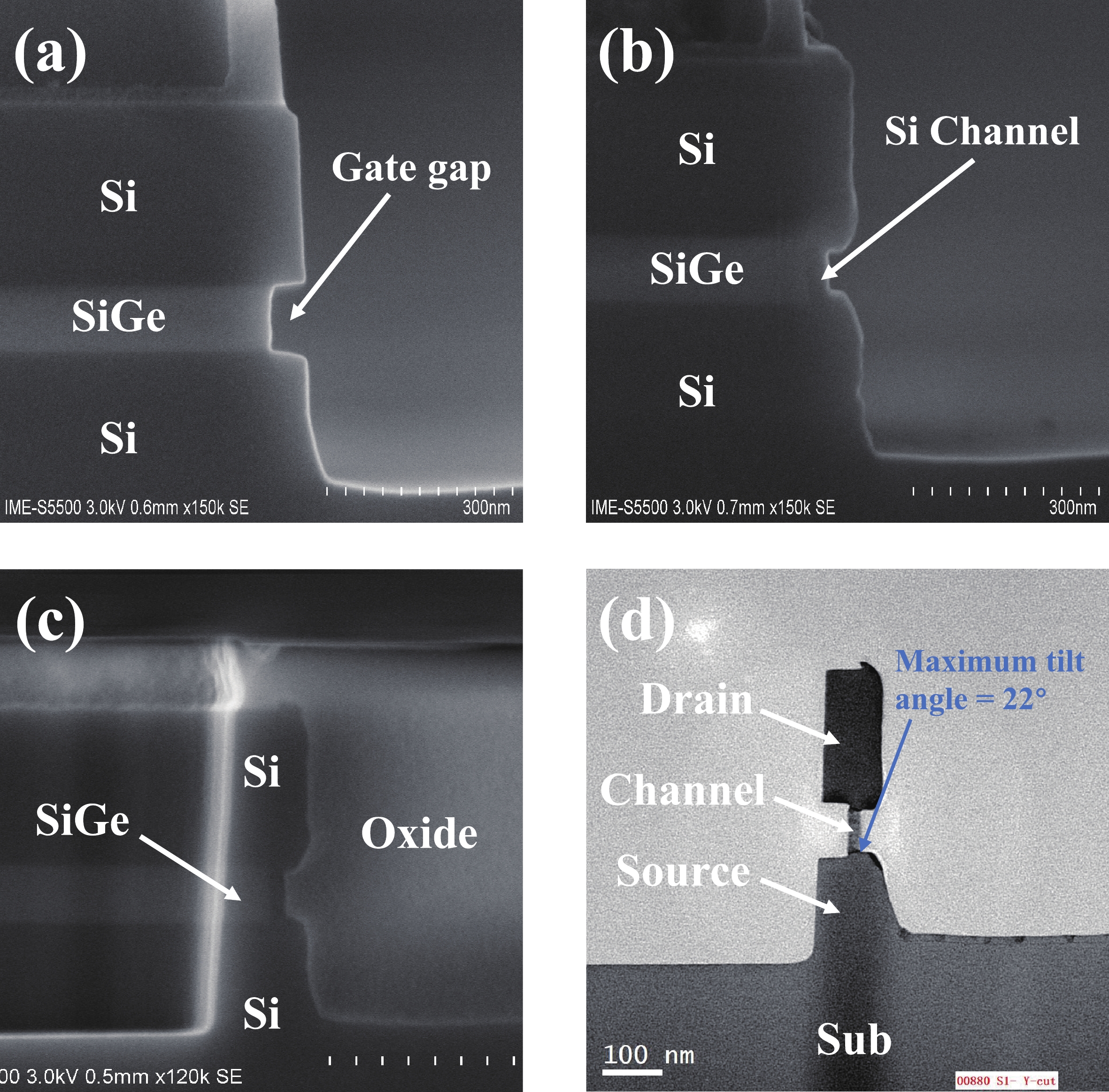
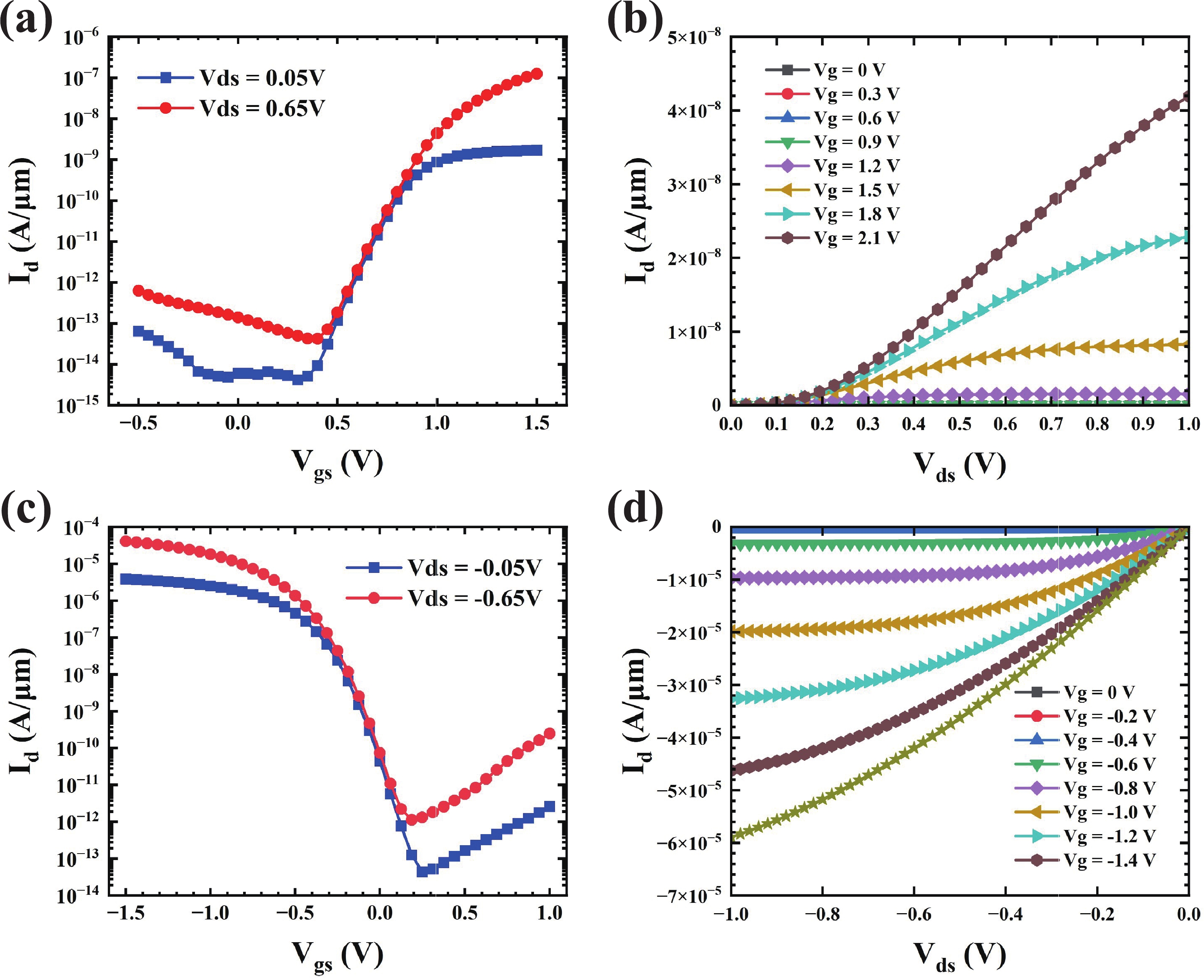
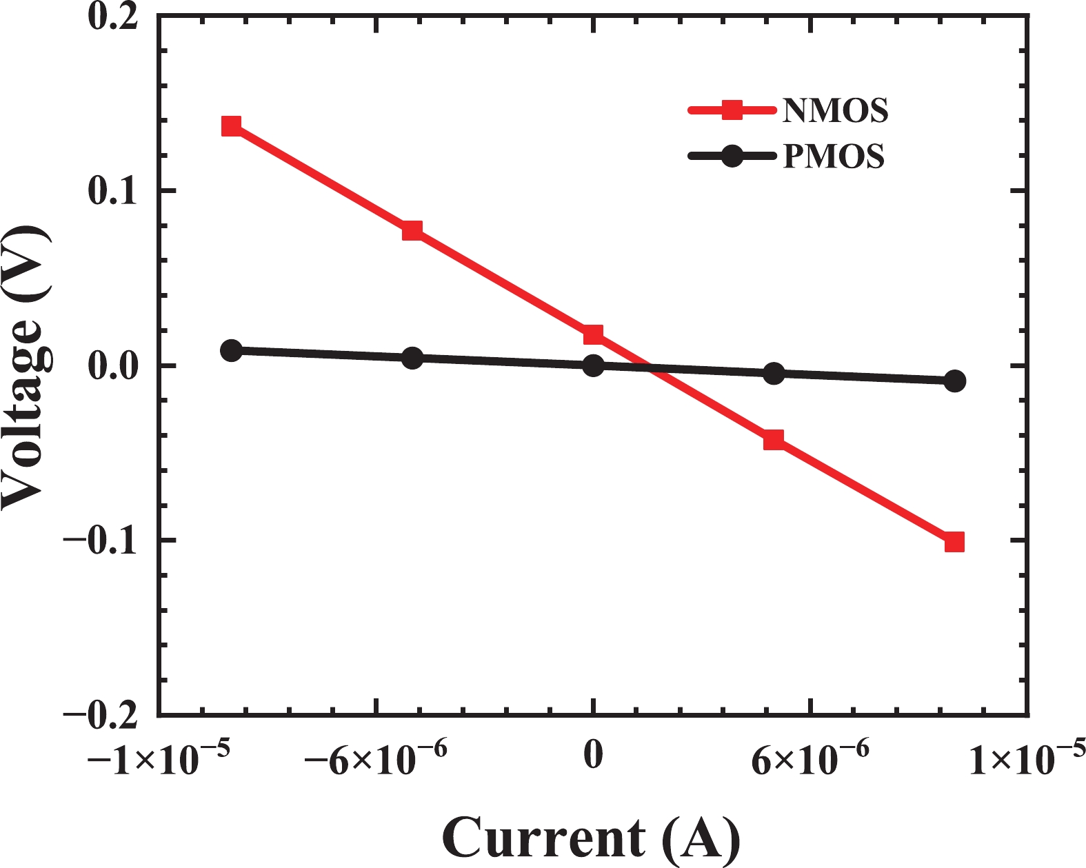
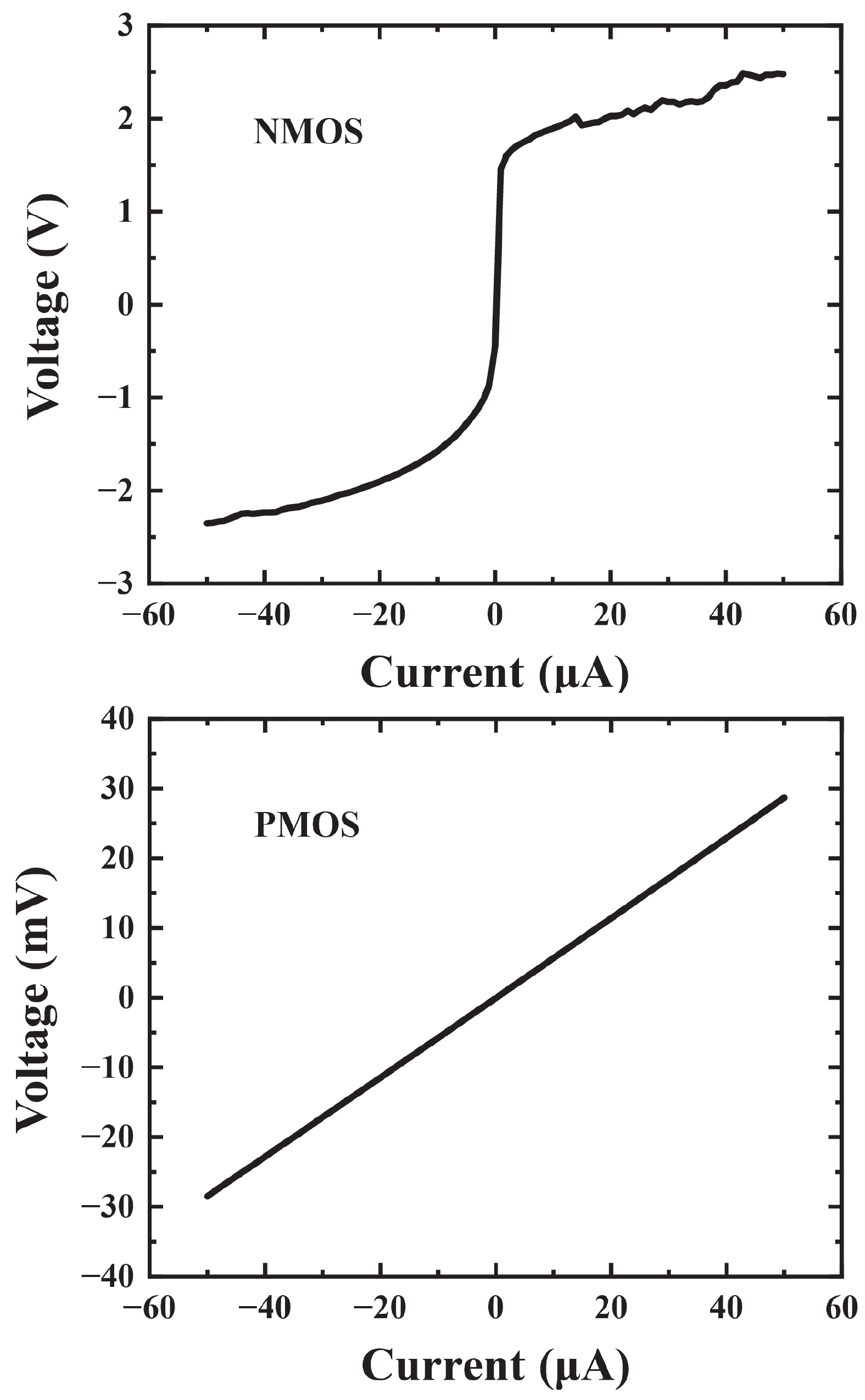
| [1] |
Takato H, Sunouchi K, Okabe N, et al. Impact of surrounding gate transistor (SGT) for ultra-high-density LSI’s. IEEE Trans Electron Devices, 1991, 38(3), 573 doi: 10.1109/16.75168 |
| [2] |
Jagannathan H, Anderson B, Sohn C W, et al. Vertical-transport nanosheet technology for CMOS scaling beyond lateral-transport devices. 2021 IEEE International Electron Devices Meeting (IEDM), 2021, 26.1.1 doi: 10.1109/IEDM19574.2021.9720561 |
| [3] |
Thean A V, Yakimets D, Huynh Bao T, et al. Vertical device architecture for 5nm and beyond: device & circuit implications. 2015 Symposium on VLSI Technology (VLSI Technology), 2015, T26 doi: 10.1109/VLSIT.2015.7223689 |
| [4] |
Yakimets D, Eneman G, Schuddinck P, et al. Vertical GAAFETs for the ultimate CMOS scaling. IEEE Trans Electron Devices, 2015, 62(5), 1433 doi: 10.1109/TED.2015.2414924 |
| [5] |
Yakimets D, Huynh Bao T, Bardon M G, et al. Lateral versus vertical gate-all-around FETs for beyond 7nm technologies. 72nd Device Research Conference, 2014, 133 doi: 10.1109/DRC.2014.6872333 |
| [6] |
Song T. Opportunities and challenges in designing and utilizing vertical nanowire FET (V-NWFET) standard cells for beyond 5 nm. IEEE Trans Nanotechnol, 2019, 18, 240 doi: 10.1109/TNANO.2019.2896362 |
| [7] |
Veloso A, Huynh-Bao T, Rosseel E, et al. Challenges and opportunities of vertical FET devices using 3D circuit design layouts. 2016 IEEE SOI-3D-Subthreshold Microelectronics Technology Unified Conference (S3S), 2016, 1 doi: 10.1109/S3S.2016.7804409 |
| [8] |
Veloso A, Altamirano-Sánchez E, Brus S, et al. (invited) vertical nanowire FET integration and device aspects. ECS Trans, 2016, 72(4), 31 doi: 10.1149/07204.0031ecst |
| [9] |
Veloso A, Eneman G, Huynh-Bao T, et al. Vertical nanowire and nanosheet FETs: device features, novel schemes for improved process control and enhanced mobility, potential for faster & more energy efficient circuits. 2019 IEEE International Electron Devices Meeting (IEDM), 2019, 11.1.1 doi: 10.1109/IEDM19573.2019.8993602 |
| [10] |
Yin X G, Zhang Y K, Zhu H L, et al. Vertical sandwich gate-all-around field-effect transistors with self-aligned high-k metal gates and small effective-gate-length variation. IEEE Electron Device Lett, 2020, 41(1), 8 doi: 10.1109/LED.2019.2954537 |
| [11] |
Zhang Y K, Ai X Z, Yin X G, et al. Vertical sandwich GAA FETs with self-aligned high-k metal gate made by quasi atomic layer etching process. IEEE Trans Electron Devices, 2021, 68(6), 2604 doi: 10.1109/TED.2021.3072879 |
| [12] |
Xiao Z R, Wang Q, Zhu H L, et al. Vertical C-shaped-channel nanosheet FETs featured with precise control of both channel-thickness and gate-length. IEEE Electron Device Lett, 2022, 43(8), 1183 doi: 10.1109/LED.2022.3187006 |
| [13] |
Li J J, Li Y L, Zhou N, et al. Study of silicon nitride inner spacer formation in process of gate-all-around nano-transistors. Nanomaterials, 2020, 10(4), 793 doi: 10.3390/nano10040793 |
| [14] |
Li C, Zhu H L, Zhang Y K, et al. First demonstration of novel vertical gate-all-around field-effect-transistors featured by self-aligned and replaced high-κ metal gates. Nano Lett, 2021, 21(11), 4730 doi: 10.1021/acs.nanolett.1c01033 |
| [15] |
Gnani E, Gnudi A, Reggiani S, et al. Theory of the junctionless nanowire FET. IEEE Trans Electron Devices, 2011, 58(9), 2903 doi: 10.1109/TED.2011.2159608 |
| [16] |
Ogura S, Tsang P J, Walker W W, et al. Design and characteristics of the lightly doped drain-source (LDD) insulated gate field-effect transistor. IEEE J Solid State Circuits, 1980, 15(4), 424 doi: 10.1109/JSSC.1980.1051416 |


 Penghui Sun got his BS degree from Central South University of Forestry and Technology in 2022. Now he is an MS student in University of Chinese Academy of Sciences under the supervision of Engineer Yongkui Zhang. His research focuses on advance CMOS technology.
 Yongkui Zhang obtained his M.s degree in 2004 in Beijing University of science and technology. He worked at Semiconductor Manufacturing International Corporation in 2004−2012. He joined the institute of Microelectronics of Chinese Academy of Sciences in 2012. His research interests are mainly focused on advanced CMOS technology research.
 DownLoad: