


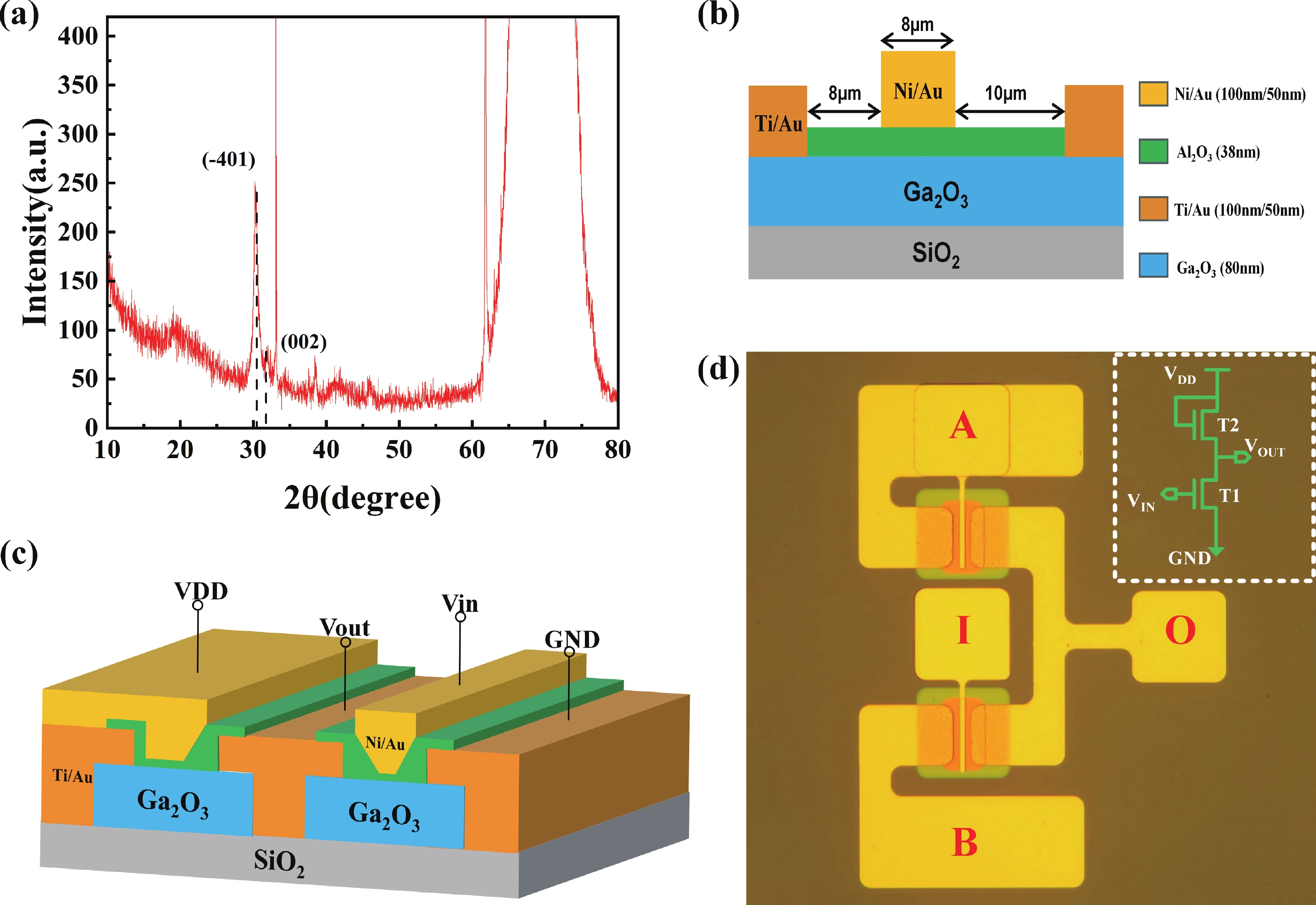
Fig. 1.
(Color online) (a) X-ray diffraction of grown β-Ga2O3; (b) illustration of structure of MOSFET; (c)illustration of structure of β-Ga2O3 inverter; (d) image of prepared β-Ga2O3 inverter.
ARTICLES
Yixin Zhang, Haifeng Chen, Zijie Ding, Yuduo Zhang, Qin Lu, Xiangtai Liu and Yunhe Guan
Corresponding author: Haifeng Chen, chenhaifeng@xupt.edu.cn
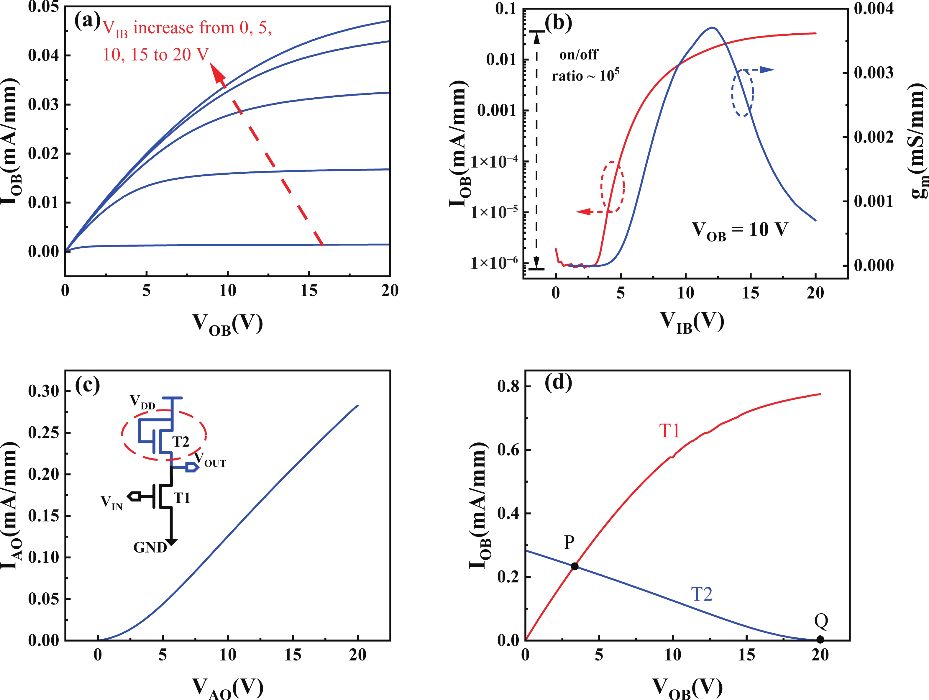
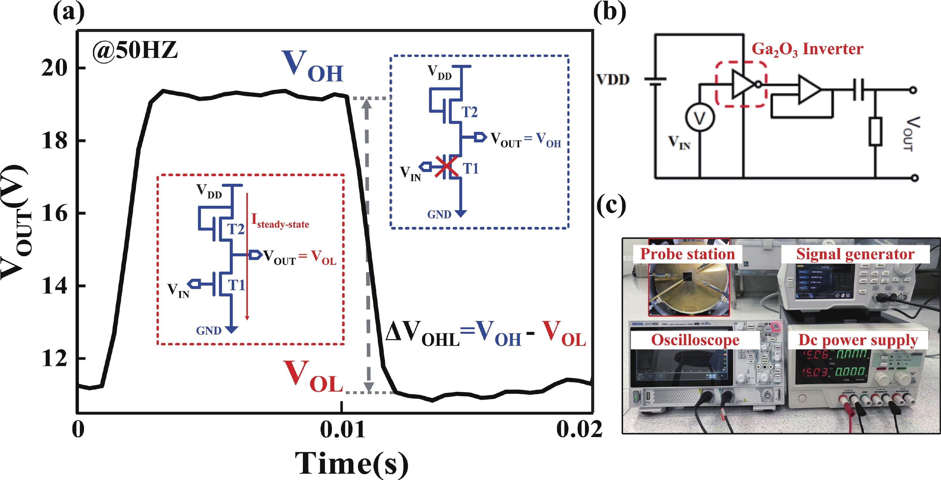
Abstract: β-Ga2O3 MOS inverter should play a crucial role in β-Ga2O3 electronic circuits. Enhancement-mode (E-mode) MOSFET was fabricated based on β-Ga2O3 film grown by atomic layer deposition technology, and the β-Ga2O3 inverter was further monolithically integrated on this basis. The β-Ga2O3 nMOSFET exhibits excellent electrical characteristics with an on/off current ratio reaching 105. The logic inverter shows outstanding voltage inversion characteristics under low-frequency from 1 to 400 Hz operation. As the frequency continues to increase to 10 K, the reverse characteristic becomes worse due to parasitic capacitance induced by processes, and the difference between the highest and lowest values of VOUT has an exponential decay relationship with the frequency. This paper provides the practice for the development of β-Ga2O3-based circuits.
Key words: ultra-wide bandgap, Ga2O3, MOSFET, inverter
| [1] |
Kim J, Kim J. Monolithically integrated enhancement-mode and depletion-mode β-Ga2O3 MESFETs with graphene-gate architectures and their logic applications. ACS Appl Mater Interfaces, 2020, 12(6): 7310 doi: 10.1021/acsami.9b19667
|
| [2] |
Qin Y, Wang Z P, Sasaki K, et al. Recent progress of Ga2O3 power technology: Large-area devices, packaging and applications. Jpn J Appl Phys, 2023, 62: SF0801 doi: 10.35848/1347-4065/acb3d3
|
| [3] |
Huang C H, Cyu R H, Chueh Y L, et al. Low-temperature pressure-assisted liquid-metal printing for β-Ga2O3 thin-film transistors. Nat Commun, 2025, 16(1): 1882 doi: 10.1038/s41467-025-57200-2
|
| [4] |
Mastro M A, Kuramata A, Calkins J, et al. Perspective: Opportunities and future directions for Ga2O3. ECS J Solid State Sci Technol, 2017, 6(5): P356 doi: 10.1149/2.0031707jss
|
| [5] |
Green A J, Chabak K D, Baldini M, et al. β-Ga2O3 MOSFETs for radio frequency operation. IEEE Electron Device Lett, 2017, 38(6): 790 doi: 10.1109/LED.2017.2694805
|
| [6] |
Guo W, Han Z, Zhao X L, et al. Large-area β-Ga2O3 Schottky barrier diode and its application in DC−DC converters. J Semicond, 2023, 44(7): 072805 doi: 10.1088/1674-4926/44/7/072805
|
| [7] |
Neudeck P G, Okojie R S, Chen L Y. High-temperature electronics-a role for wide bandgap semiconductors? Proc IEEE, 2002, 90(6): 1065 doi: 10.1109/JPROC.2002.1021571
|
| [8] |
Cai Y, Cheng Z Q, Yang Z C, et al. High-temperature operation of AlGaN/GaN HEMTs direct-coupled FET logic (DCFL) integrated circuits. IEEE Electron Device Lett, 2007, 28(5): 328 doi: 10.1109/LED.2007.895391
|
| [9] |
Khandelwal V, Yuvaraja S, García G I M, et al. Monolithic β-Ga2O3 nmos IC based on heteroepitaxial E-mode MOSFETs. Appl Phys Lett, 2023, 122(14): 143502 doi: 10.1063/5.0143315
|
| [10] |
Chettri D, Mainali G, Xiao N, et al. Monolithic n-type metal−oxide−semiconductor inverter integrated circuits based on wide and ultrawide bandgap semiconductors. Phys Status Solidi B, 2024, 261(7): 2300493 doi: 10.1002/pssb.202300493
|
| [11] |
Chettri D, Mainali G, Salcedo J H, et al. Demonstration of normally OFF beta-gallium oxide monolithic bidirectional switch for AC switching applications. Appl Phys Lett, 2024, 125(20): 202104 doi: 10.1063/5.0237484
|
| [12] |
Singh R, Lenka T R, Velpula R T, et al. Investigation of current collapse and recovery time due to deep level defect traps in β-Ga2O3 HEMT. J Semicond, 2020, 41(10): 102802 doi: 10.1088/1674-4926/41/10/102802
|
| [13] |
Bader S J, Lee H, Chaudhuri R, et al. Prospects for wide bandgap and ultrawide bandgap CMOS devices. IEEE Trans Electron Devices, 2020, 67(10): 4010 doi: 10.1109/TED.2020.3010471
|
| [14] |
Park J H, McClintock R, Razeghi M. Ga2O3 metal-oxide-semiconductor field effect transistors on sapphire substrate by MOCVD. Semicond Sci Technol, 2019, 34(8): 08LT01 doi: 10.1088/1361-6641/ab2c17
|
| [15] |
Jeong Y J, Yang J Y, Lee C H, et al. Fluorine-based plasma treatment for hetero-epitaxial β-Ga2O3 MOSFETs. Appl Surf Sci, 2021, 558: 149936 doi: 10.1016/j.apsusc.2021.149936
|
| [16] |
Zhou H, Si M W, Alghamdi S, et al. High-performance depletion/enhancement-ode β-Ga2O3 on insulator (GOOI) field-effect transistors with record drain currents of 600/450 mA/mm. IEEE Electron Device Lett, 2017, 38(1): 103 doi: 10.1109/LED.2016.2635579
|
| [17] |
Zhao W P, Han L X, Zhang N, et al. High-gain transparent inverters based on deuterated ZnO TFTs fabricated by atomic layer deposition. IEEE Electron Device Lett, 2020, 41(10): 1508 doi: 10.1109/LED.2020.3018443
|
| [18] |
Kim J S, Jang J H, Kim Y D, et al. Dynamic logic circuits using a-IGZO TFTs. IEEE Trans Electron Devices, 2017, 64(10): 4123 doi: 10.1109/TED.2017.2738665
|
| [19] |
Zheng Z Y, Zhang L, Song W J, et al. Gallium nitride-based complementary logic integrated circuits. Nat Electron, 2021, 4: 595 doi: 10.1038/s41928-021-00611-y
|
| [20] |
Jiang J L, Luo J S, Ding K, et al. High-performance broad-spectrum UV photodetectors with uniform response: Engineering β-Ga2O3: Si/GaN: Si heterojunctions via thermal oxidation for optoelectronic logic gate and multispectral imaging. Small, 2025, 21(12): e2406447 doi: 10.1002/smll.202406447
|
| [21] |
Garcia R, Rodriguez-Lopez O, Rocha-Flores P E, et al. Impact of applied voltage on threshold voltage instability in active load thin-film a-IGZO inverters. IEEE Trans Electron Devices, 2023, 70(8): 4220 doi: 10.1109/TED.2023.3288074
|
| [22] |
Okada H, Miwa K, Yokoyama T, et al. GaN-based monolithic inverter consisting of enhancement- and depletion-mode MOSFETs by Si ion implantation. Phys Status Solidi A, 2020, 217(3): 1900550 doi: 10.1002/pssa.201900550
|
| [23] |
Zhu M H, Matioli E. Monolithic integration of GaN-based NMOS digital logic gate circuits with E-mode power GaN MOSHEMTs. 2018 IEEE 30th International Symposium on Power Semiconductor Devices and ICs (ISPSD), 2018: 236 doi: 10.1109/ISPSD.2018.8393646
|
| [24] |
Zhang B, Wang J Y, Wang C, et al. Monolithic integration of GaN-based enhancement/depletion-mode MIS-HEMTs with AlN/SiN bilayer dielectric. IEEE Electron Device Lett, 2022, 43(7): 1025 doi: 10.1109/LED.2022.3180049
|
| [25] |
Liu C Y, Wang Y B, Xu W H, et al. Unique bias stress instability of heterogeneous Ga2O3-on-SiC MOSFET. IEEE Electron Device Lett, 2023, 44(8): 1256 doi: 10.1109/LED.2023.3288820
|
| [26] |
Liu C Y, Li B C, Wang Y B, et al. Unique monotonic positive shifts in threshold voltages of Ga2O3-on-SiC MOSFETs under both unipolar positive and negative bias stresses. IEEE Trans Electron Devices, 2025, 72(3): 1047 doi: 10.1109/TED.2025.3534742
|


Article views: 1374 Times PDF downloads: 130 Times Cited by: 0 Times
Received: 11 April 2025 Revised: 23 July 2025 Online: Accepted Manuscript: 08 September 2025Uncorrected proof: 15 September 2025Published: 15 February 2026
| Citation: |
Yixin Zhang, Haifeng Chen, Zijie Ding, Yuduo Zhang, Qin Lu, Xiangtai Liu, Yunhe Guan. Characteristics of gallium oxide nMOSFET inverter[J]. Journal of Semiconductors, 2026, 47(2): 022302. doi: 10.1088/1674-4926/25040011
****
Y X Zhang, H F Chen, Z J Ding, Y D Zhang, Q Lu, X T Liu, and Y H Guan, Characteristics of gallium oxide nMOSFET inverter[J]. J. Semicond., 2026, 47(2): 022302 doi: 10.1088/1674-4926/25040011

|
 Yixin Zhang received her BS degree from Xianmen University of Technology in 2023. She is currently a Master's student at Xian University of Posts and telecommunication. Her research focuses on Ga2O3 power devices
 Haifeng Chen received the Ph.D. degree from Xidian University in 2008. He is currently a Professor at the Xi’an University of Posts and Telecommunications. His research interests focus on Ga2O3 material and devices
 Zijie Ding is currently a master's student at Xi'an University of Posts and Telecommunications. He is in his third year in the School of Electronic Engineering, and his research primarily focuses on devices based on β-Ga2O3 nanobelts
| [1] |
Kim J, Kim J. Monolithically integrated enhancement-mode and depletion-mode β-Ga2O3 MESFETs with graphene-gate architectures and their logic applications. ACS Appl Mater Interfaces, 2020, 12(6): 7310 doi: 10.1021/acsami.9b19667
|
| [2] |
Qin Y, Wang Z P, Sasaki K, et al. Recent progress of Ga2O3 power technology: Large-area devices, packaging and applications. Jpn J Appl Phys, 2023, 62: SF0801 doi: 10.35848/1347-4065/acb3d3
|
| [3] |
Huang C H, Cyu R H, Chueh Y L, et al. Low-temperature pressure-assisted liquid-metal printing for β-Ga2O3 thin-film transistors. Nat Commun, 2025, 16(1): 1882 doi: 10.1038/s41467-025-57200-2
|
| [4] |
Mastro M A, Kuramata A, Calkins J, et al. Perspective: Opportunities and future directions for Ga2O3. ECS J Solid State Sci Technol, 2017, 6(5): P356 doi: 10.1149/2.0031707jss
|
| [5] |
Green A J, Chabak K D, Baldini M, et al. β-Ga2O3 MOSFETs for radio frequency operation. IEEE Electron Device Lett, 2017, 38(6): 790 doi: 10.1109/LED.2017.2694805
|
| [6] |
Guo W, Han Z, Zhao X L, et al. Large-area β-Ga2O3 Schottky barrier diode and its application in DC−DC converters. J Semicond, 2023, 44(7): 072805 doi: 10.1088/1674-4926/44/7/072805
|
| [7] |
Neudeck P G, Okojie R S, Chen L Y. High-temperature electronics-a role for wide bandgap semiconductors? Proc IEEE, 2002, 90(6): 1065 doi: 10.1109/JPROC.2002.1021571
|
| [8] |
Cai Y, Cheng Z Q, Yang Z C, et al. High-temperature operation of AlGaN/GaN HEMTs direct-coupled FET logic (DCFL) integrated circuits. IEEE Electron Device Lett, 2007, 28(5): 328 doi: 10.1109/LED.2007.895391
|
| [9] |
Khandelwal V, Yuvaraja S, García G I M, et al. Monolithic β-Ga2O3 nmos IC based on heteroepitaxial E-mode MOSFETs. Appl Phys Lett, 2023, 122(14): 143502 doi: 10.1063/5.0143315
|
| [10] |
Chettri D, Mainali G, Xiao N, et al. Monolithic n-type metal−oxide−semiconductor inverter integrated circuits based on wide and ultrawide bandgap semiconductors. Phys Status Solidi B, 2024, 261(7): 2300493 doi: 10.1002/pssb.202300493
|
| [11] |
Chettri D, Mainali G, Salcedo J H, et al. Demonstration of normally OFF beta-gallium oxide monolithic bidirectional switch for AC switching applications. Appl Phys Lett, 2024, 125(20): 202104 doi: 10.1063/5.0237484
|
| [12] |
Singh R, Lenka T R, Velpula R T, et al. Investigation of current collapse and recovery time due to deep level defect traps in β-Ga2O3 HEMT. J Semicond, 2020, 41(10): 102802 doi: 10.1088/1674-4926/41/10/102802
|
| [13] |
Bader S J, Lee H, Chaudhuri R, et al. Prospects for wide bandgap and ultrawide bandgap CMOS devices. IEEE Trans Electron Devices, 2020, 67(10): 4010 doi: 10.1109/TED.2020.3010471
|
| [14] |
Park J H, McClintock R, Razeghi M. Ga2O3 metal-oxide-semiconductor field effect transistors on sapphire substrate by MOCVD. Semicond Sci Technol, 2019, 34(8): 08LT01 doi: 10.1088/1361-6641/ab2c17
|
| [15] |
Jeong Y J, Yang J Y, Lee C H, et al. Fluorine-based plasma treatment for hetero-epitaxial β-Ga2O3 MOSFETs. Appl Surf Sci, 2021, 558: 149936 doi: 10.1016/j.apsusc.2021.149936
|
| [16] |
Zhou H, Si M W, Alghamdi S, et al. High-performance depletion/enhancement-ode β-Ga2O3 on insulator (GOOI) field-effect transistors with record drain currents of 600/450 mA/mm. IEEE Electron Device Lett, 2017, 38(1): 103 doi: 10.1109/LED.2016.2635579
|
| [17] |
Zhao W P, Han L X, Zhang N, et al. High-gain transparent inverters based on deuterated ZnO TFTs fabricated by atomic layer deposition. IEEE Electron Device Lett, 2020, 41(10): 1508 doi: 10.1109/LED.2020.3018443
|
| [18] |
Kim J S, Jang J H, Kim Y D, et al. Dynamic logic circuits using a-IGZO TFTs. IEEE Trans Electron Devices, 2017, 64(10): 4123 doi: 10.1109/TED.2017.2738665
|
| [19] |
Zheng Z Y, Zhang L, Song W J, et al. Gallium nitride-based complementary logic integrated circuits. Nat Electron, 2021, 4: 595 doi: 10.1038/s41928-021-00611-y
|
| [20] |
Jiang J L, Luo J S, Ding K, et al. High-performance broad-spectrum UV photodetectors with uniform response: Engineering β-Ga2O3: Si/GaN: Si heterojunctions via thermal oxidation for optoelectronic logic gate and multispectral imaging. Small, 2025, 21(12): e2406447 doi: 10.1002/smll.202406447
|
| [21] |
Garcia R, Rodriguez-Lopez O, Rocha-Flores P E, et al. Impact of applied voltage on threshold voltage instability in active load thin-film a-IGZO inverters. IEEE Trans Electron Devices, 2023, 70(8): 4220 doi: 10.1109/TED.2023.3288074
|
| [22] |
Okada H, Miwa K, Yokoyama T, et al. GaN-based monolithic inverter consisting of enhancement- and depletion-mode MOSFETs by Si ion implantation. Phys Status Solidi A, 2020, 217(3): 1900550 doi: 10.1002/pssa.201900550
|
| [23] |
Zhu M H, Matioli E. Monolithic integration of GaN-based NMOS digital logic gate circuits with E-mode power GaN MOSHEMTs. 2018 IEEE 30th International Symposium on Power Semiconductor Devices and ICs (ISPSD), 2018: 236 doi: 10.1109/ISPSD.2018.8393646
|
| [24] |
Zhang B, Wang J Y, Wang C, et al. Monolithic integration of GaN-based enhancement/depletion-mode MIS-HEMTs with AlN/SiN bilayer dielectric. IEEE Electron Device Lett, 2022, 43(7): 1025 doi: 10.1109/LED.2022.3180049
|
| [25] |
Liu C Y, Wang Y B, Xu W H, et al. Unique bias stress instability of heterogeneous Ga2O3-on-SiC MOSFET. IEEE Electron Device Lett, 2023, 44(8): 1256 doi: 10.1109/LED.2023.3288820
|
| [26] |
Liu C Y, Li B C, Wang Y B, et al. Unique monotonic positive shifts in threshold voltages of Ga2O3-on-SiC MOSFETs under both unipolar positive and negative bias stresses. IEEE Trans Electron Devices, 2025, 72(3): 1047 doi: 10.1109/TED.2025.3534742
|

 WeChat ID
Journal of Semiconductors © 2017 All Rights Reserved 京ICP备05085259号-2

 DownLoad:

