Fig. 1.
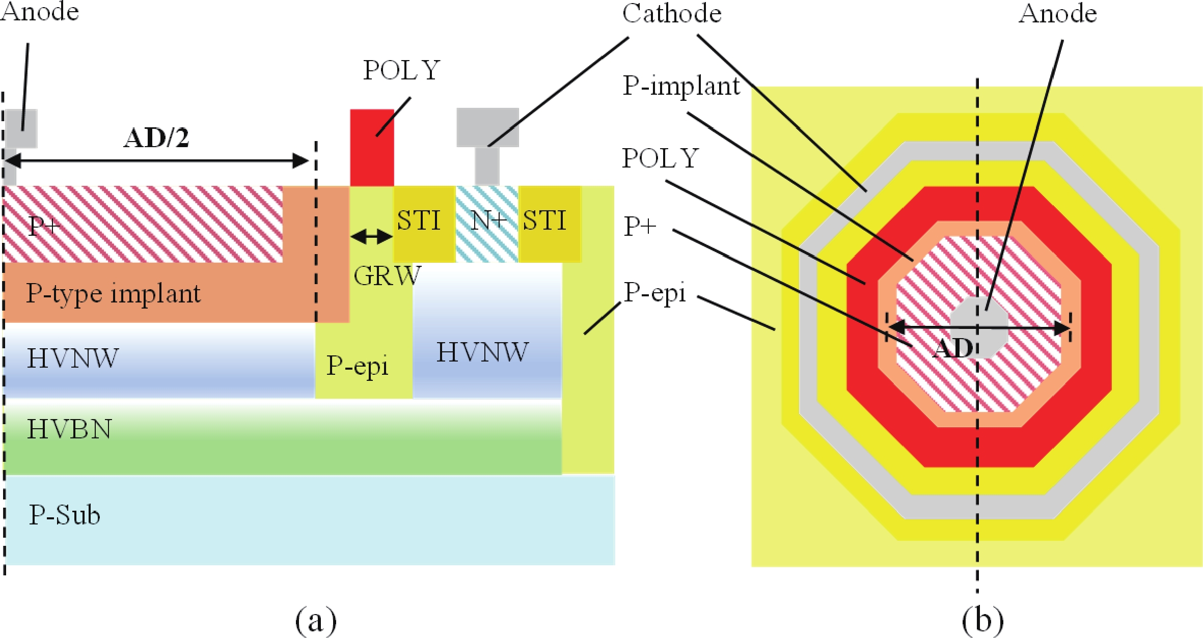
(Color online) The structure of the p-type implant/HVNW SPAD. (a) Semi-cross-sectional view; (b) top view.
ARTICLES
Zhentao Ni1, Dajing Bian1, Haoxiang Jiang1, Xiaoming Huang1, 2 and Yue Xu1, 2,
Corresponding author: Yue Xu, yuex@njupt.edu.cn
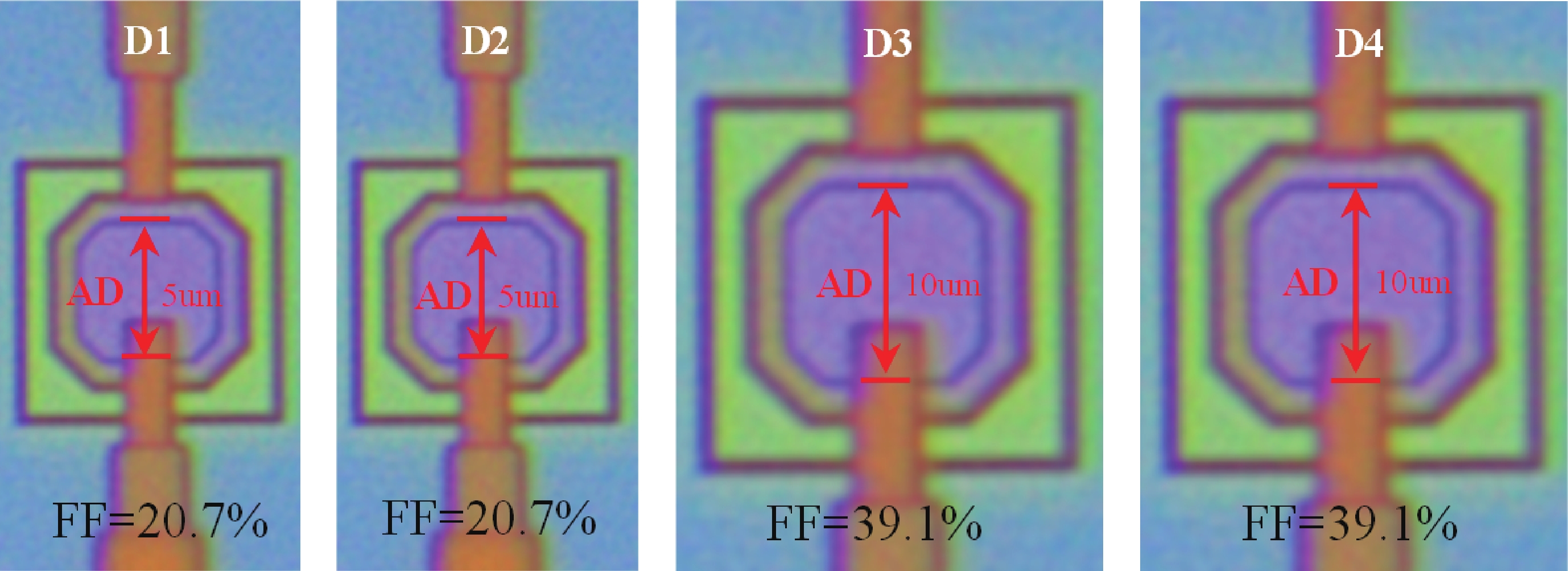
Abstract: A high-sensitivity, low-noise single photon avalanche diode (SPAD) detector was presented based on a 180 nm BCD process. The proposed device utilizes a p-implant layer/high-voltage n-well (HVNW) junction to form a deep avalanche multiplication region for near-infrared (NIR) sensitivity enhancement. By optimizing the device size and electric field of the guard ring, the fill factor (FF) is significantly improved, further increasing photon detection efficiency (PDE). To solve the dark noise caused by the increasing active diameter, a field polysilicon gate structure connected to the p+ anode was investigated, effectively suppressing dark count noise by 76.6%. It is experimentally shown that when the active diameter increases from 5 to 10 μm, the FF is significantly improved from 20.7% to 39.1%, and thus the peak PDE also rises from 13.3% to 25.8%. At an excess bias voltage of 5 V, a NIR photon detection probability (PDP) of 6.8% at 905 nm, a dark count rate (DCR) of 2.12 cps/μm2, an afterpulsing probability (AP) of 1.2%, and a timing jitter of 216 ps are achieved, demonstrating excellent single photon detection performance.
Key words: single-photon avalanche diode (SPAD), fill factor (FF), photon detection efficiency (PDE), dark count rate (DCR)
| [1] |
Wayne M, Ulku A, Ardelean A, et al. A 500 × 500 dual-gate SPAD imager with 100% temporal aperture and 1 ns minimum gate length for FLIM and phasor imaging applications. IEEE Trans Electron Devices, 2022, 69(6): 2865 doi: 10.1109/TED.2022.3168249
|
| [2] |
Hutchings S W, Johnston N, Gyongy I, et al. A reconfigurable 3-D-stacked SPAD imager with in-pixel histogramming for flash LIDAR or high-speed time-of-flight imaging. IEEE J Solid State Circuits, 2019, 54(11): 2947 doi: 10.1109/JSSC.2019.2939083
|
| [3] |
Vornicu I, López-Martínez J M, Bandi F N, et al. Design of high-efficiency SPADs for LiDAR applications in 110nm CIS technology. IEEE Sens J, 2021, 21(4): 4776 doi: 10.1109/JSEN.2020.3032106
|
| [4] |
Katz A, Blank T, Fenigstein A, et al. Active-reset for the N P single-ended SPAD used in the NIR LiDAR receivers. IEEE Trans Electron Devices, 2019, 66(12): 5191 doi: 10.1109/TED.2019.2946015
|
| [5] |
Park E, Eom D, Kim J H, et al. Back-illuminated SPAD in 40 nm CIS technology achieving 56 ps timing jitter with 15 V breakdown voltage for short/mid-range LiDAR applications. 2023 International Electron Devices Meeting (IEDM), 2023: 1 doi: 10.1109/IEDM45741.2023.10413695
|
| [6] |
Gebremicael K N, Rarity J G, Sibson P. Capacitive response signal cancellation for sine wave gated high-speed single photon avalanche photodiode detector. IEEE J Quantum Electron, 2021, 57(4): 4500305 doi: 10.1109/JQE.2021.3078737
|
| [7] |
Wen G H, Huang J, Zhang L, et al. A high-speed and high-sensitivity photon-counting communication system based on multichannel SPAD detection. IEEE Photonics J, 2021, 13(2): 7900310 doi: 10.1109/JPHOT.2021.3058002
|
| [8] |
Huang J, Li C K, Dai J S, et al. Real-time and high-speed underwater photon-counting communication based on SPAD and PPM symbol synchronization. IEEE Photonics J, 2021, 13(5): 7300209 doi: 10.1109/JPHOT.2021.3113659
|
| [9] |
Veerappan C, Charbon E. CMOS SPAD based on photo-carrier diffusion achieving PDP >40% from 440 to 580 nm at 4 V excess bias. IEEE Photonics Technol Lett, 2015, 27(23): 2445 doi: 10.1109/LPT.2015.2468067
|
| [10] |
Park E, Eom D, Yu M H, et al. Back-illuminated double-avalanche-region single-photon avalanche diode. IEEE J Sel Top Quantum Electron, 2024, 30(1): 3800809 doi: 10.1109/JSTQE.2023.3322354
|
| [11] |
Sun W B, Wang Y X, Liu M L, et al. A back-illuminated 4μm P+N-well single photon avalanche diode pixel array with 0.36Hz/μm2 dark count rate at 2.5 V excess bias voltage. IEEE Electron Device Lett, 2022, 43(9): 1519 doi: 10.1109/LED.2022.3196172
|
| [12] |
Van Sieleghem E, Karve G, De Munck K, et al. A backside-illuminated charge-focusing silicon SPAD with enhanced near-infrared sensitivity. IEEE Trans Electron Devices, 2022, 69(3): 1129 doi: 10.1109/TED.2022.3143487
|
| [13] |
Lindner S, Pellegrini S, Henrion Y, et al. A high-PDE, backside-illuminated SPAD in 65/40-nm 3D IC CMOS pixel with cascoded passive quenching and active recharge. IEEE Electron Device Lett, 2017, 38(11): 1547 doi: 10.1109/LED.2017.2755989
|
| [14] |
Jang J, Kim J, Oh S, et al. A 336 × 240 backside-illuminated 3D-stacked 7μm SPAD for LiDAR sensor with PDE 28% at 940nm and under 0.4% depth accuracy up to 10m. 2024 IEEE Symposium on VLSI Technology and Circuits (VLSI Technology and Circuits), 2024: 1 doi: 10.1109/VLSITechnologyandCir46783.2024.10631458
|
| [15] |
Gyongy I, Calder N, Davies A, et al. A 256 × 256, 100-kfps, 61% fill-factor SPAD image sensor for time-resolved microscopy applications. IEEE Trans Electron Devices, 2018, 65(2): 547 doi: 10.1109/TED.2017.2779790
|
| [16] |
Wu J Y, Liu C H. Design and characterization of n/p-well CMOS SPAD with low dark count rate and high photon detection efficiency. IEEE Trans Electron Devices, 2023, 70(2): 582 doi: 10.1109/TED.2022.3231575
|
| [17] |
Lu X, Law M K, Jiang Y, et al. A 4-μm diameter SPAD using less-doped N-well guard ring in baseline 65-nm CMOS. IEEE Trans Electron Devices, 2020, 67(5): 2223 doi: 10.1109/TED.2020.2982701
|
| [18] |
Wang Y, Jin X L, Cao S G, et al. Design and measurement of ring-gate single photon avalanche diode with low dark count rate. IEEE Photonics J, 2020, 12(3): 6801711 doi: 10.1109/JPHOT.2020.2993654
|
| [19] |
Liu D L, Li M, Xu T, et al. Study of the influence of virtual guard ring width on the performance of SPAD detectors in 180 nm standard CMOS technology. J Semicond, 2023, 44(11): 114102 doi: 10.1088/1674-4926/44/11/114102
|
| [20] |
Jiang W, Scott R, Deen M J. Improved noise performance of CMOS poly gate single-photon avalanche diodes. IEEE Photonics J, 2022, 14(1): 6802208 doi: 10.1109/JPHOT.2021.3128055
|
| [21] |
Jinseok O, Chanho K, MinSun L, et al. Optimization and calibration of the single photon avalanche diode (SPAD) for integrated on-chip sensor interface in common CMOS process. 2023 IEEE Nuclear Science Symposium, Medical Imaging Conference and International Symposium on Room-Temperature Semiconductor Detectors (NSS MIC RTSD), 2023: 1 doi: 10.1109/NSSMICRTSD49126.2023.10338770
|
| [22] |
Gramuglia F, Keshavarzian P, Kizilkan E, et al. Engineering breakdown probability profile for PDP and DCR optimization in a SPAD fabricated in a standard 55 nm BCD process. IEEE J Sel Top Quantum Electron, 2022, 28(2): 3802410 doi: 10.1109/JSTQE.2021.3114346
|
| [23] |
Liu Y, Fan R Q, Zhao Y H, et al. Junction-optimized SPAD with 50.6% peak PDP and 0.64 cps/μm2 DCR at 2 V excess bias voltage in 130 nm CMOS. IEEE Electron Device Lett, 2024, 45(3): 308 doi: 10.1109/LED.2024.3356123
|
| [24] |
Wu J Y, Liu C H. Designing a sub-20V breakdown voltage SPAD with standard CMOS technology and n/p-well structure. IEEE Photonics J, 2024, 16(2): 6800408 doi: 10.1109/JPHOT.2024.3361732
|
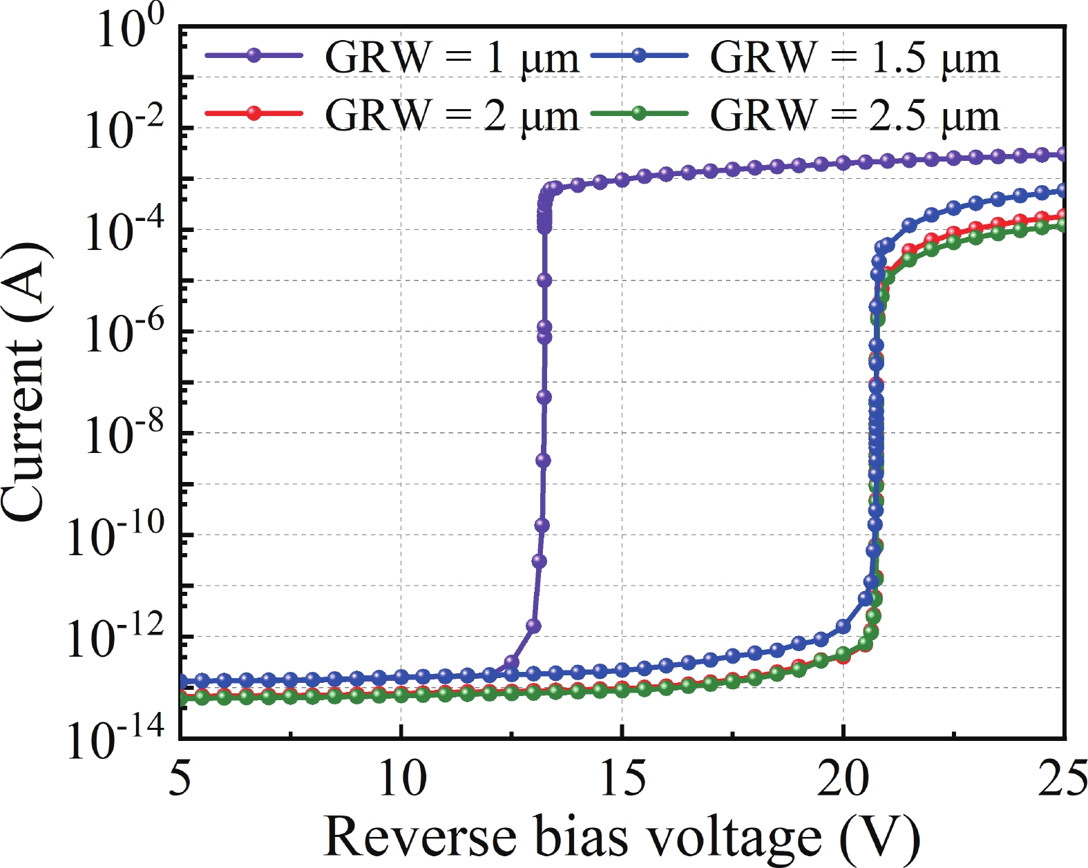
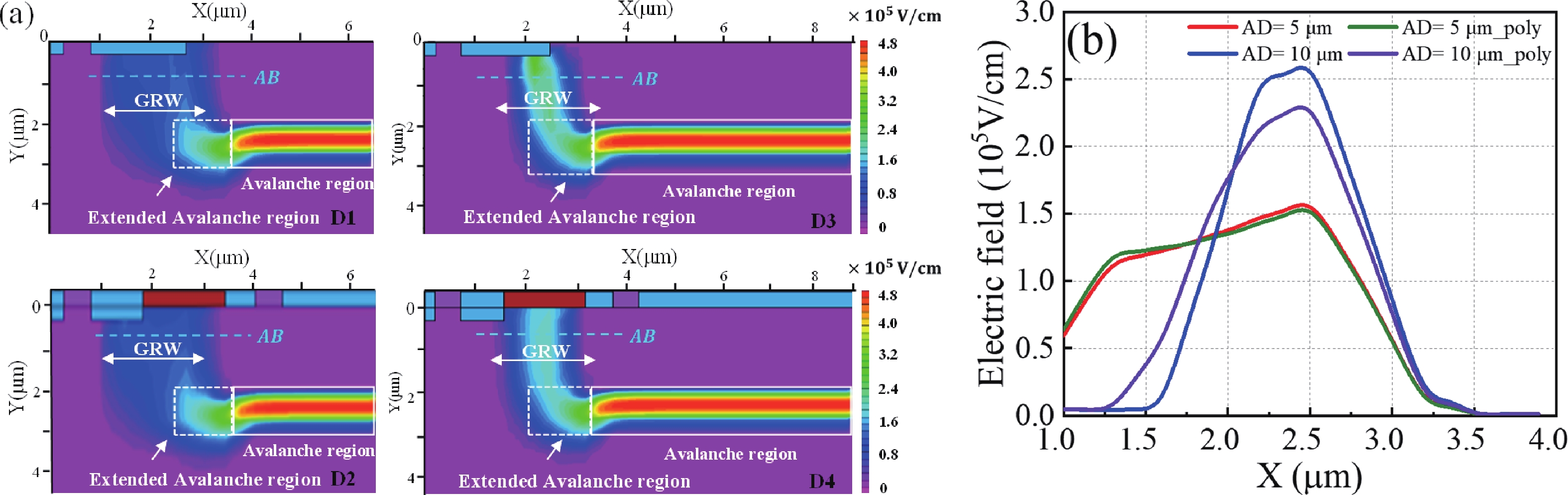
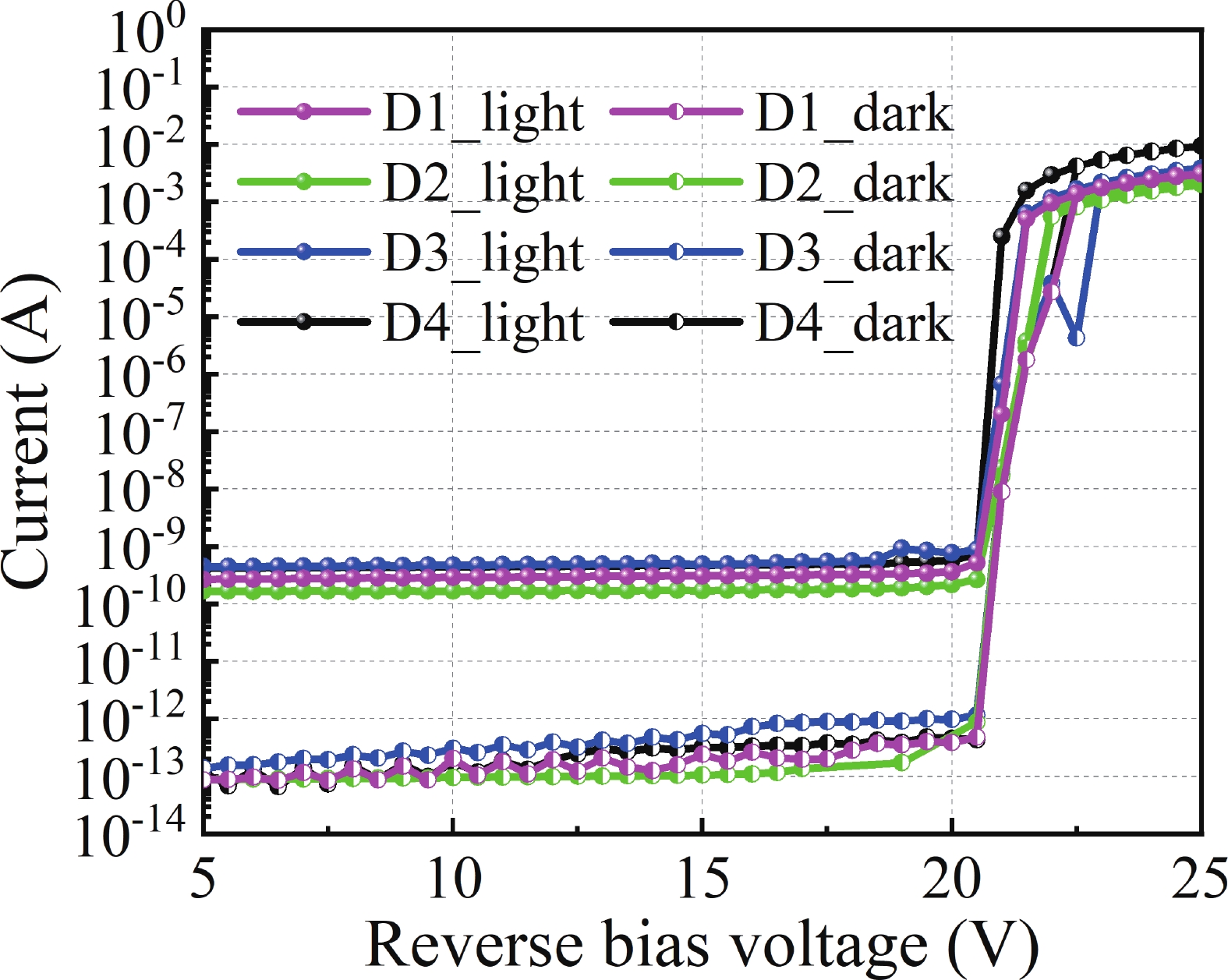
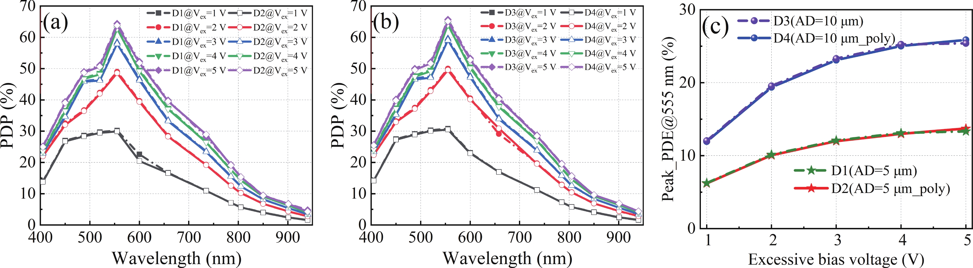
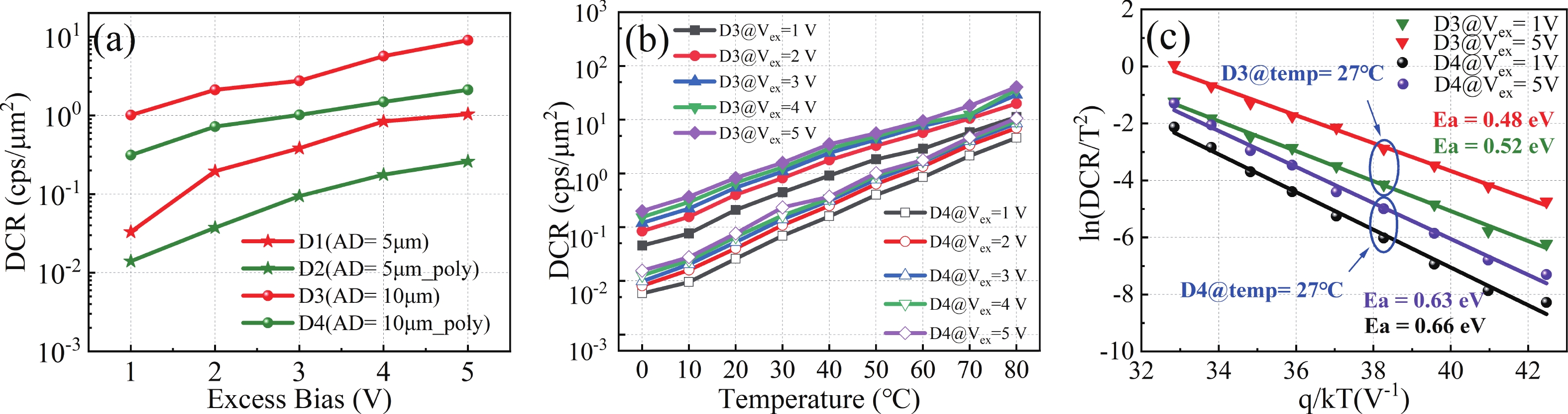
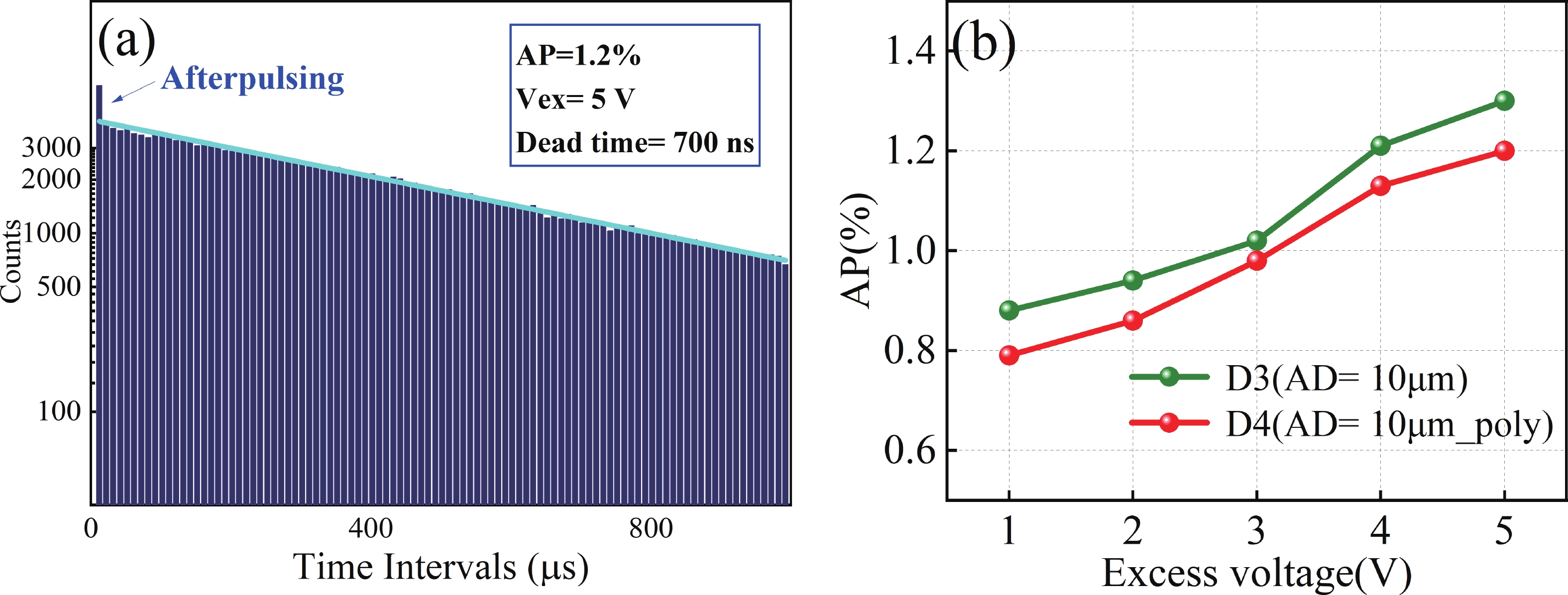
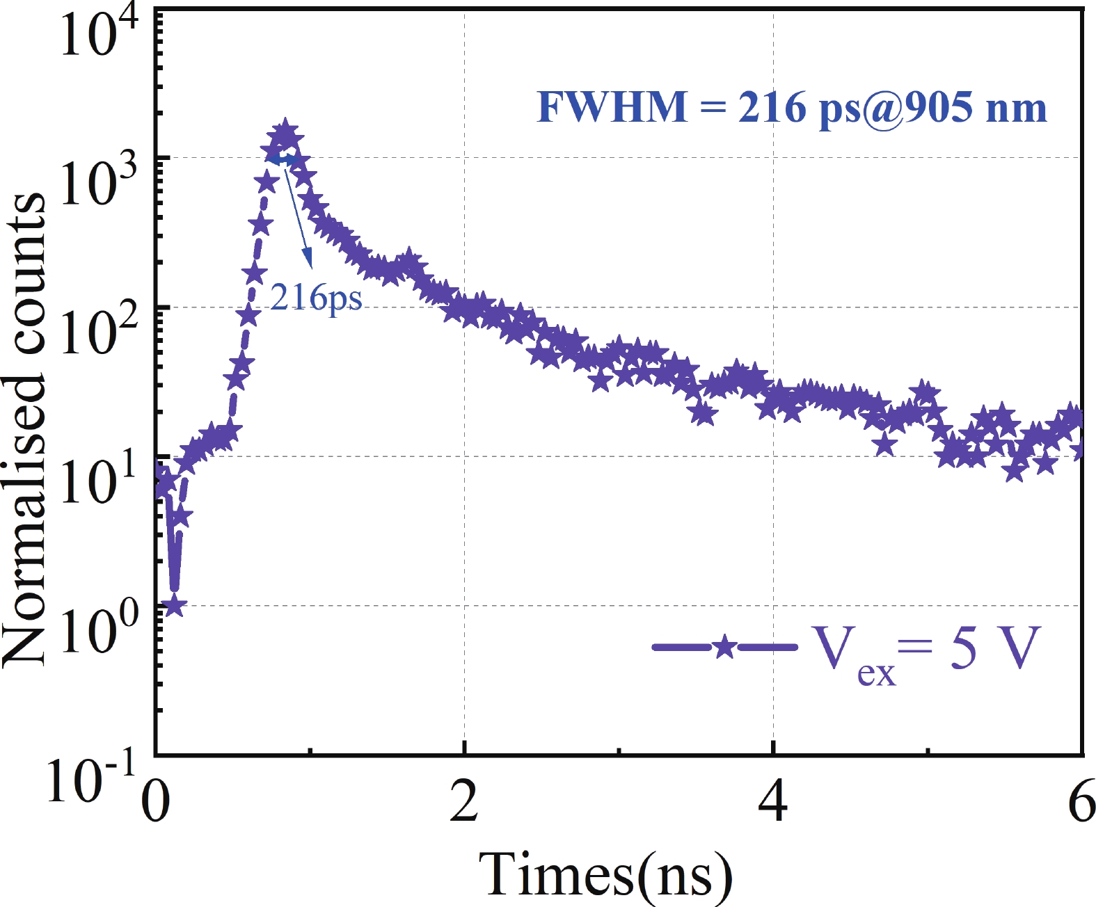
Table 1. Comparison with the state-of-the-art SPADs.
| Parameter | Ref. [11] | Ref. [20] | Ref. [22] | Ref. [23] | Ref. [24] | This work |
| Process | BSI 55 nm | FSI 180 nm | FSI 55 nm | FSI 130 nm | FSI 180 nm | FSI 180 nm |
| Structure | P+/N-well | N+/P-well | DPW/BNW | PW/DNW | N+/P-well | P-type/HVNW |
| VBD (V) | 20.5 | 12.14 | 31.5 | 16 | 18.2 | 21 |
| FF (%) | 41.6% | 32.7% | 25.2% | 39% | N/A | 39.1% |
| DCR (cps/μm2)@Vex (V) | 0.36@2.5 | 629@0.5 | 2.6@7 | 1.01@2.5 | 90@3.64 | 2.12@5 |
| AP (%) @ dead time (ns) | N/A | 4.94@5000 | ~0.97@4.5 | 0.16@15 | 4.2@N/A | 1.2@700 |
| Peak PDP (%) @ λ (nm) | 25.2@625 | 7.35@560 | 62@530 | 50.6@505 | 30@600 | 65.1@555 |
| PDP (%) @ 905 nm | 12 | <2 | ~5 | 5.05 | 15 | 6.8 |
 DownLoad: CSV
| [1] |
Wayne M, Ulku A, Ardelean A, et al. A 500 × 500 dual-gate SPAD imager with 100% temporal aperture and 1 ns minimum gate length for FLIM and phasor imaging applications. IEEE Trans Electron Devices, 2022, 69(6): 2865 doi: 10.1109/TED.2022.3168249
|
| [2] |
Hutchings S W, Johnston N, Gyongy I, et al. A reconfigurable 3-D-stacked SPAD imager with in-pixel histogramming for flash LIDAR or high-speed time-of-flight imaging. IEEE J Solid State Circuits, 2019, 54(11): 2947 doi: 10.1109/JSSC.2019.2939083
|
| [3] |
Vornicu I, López-Martínez J M, Bandi F N, et al. Design of high-efficiency SPADs for LiDAR applications in 110nm CIS technology. IEEE Sens J, 2021, 21(4): 4776 doi: 10.1109/JSEN.2020.3032106
|
| [4] |
Katz A, Blank T, Fenigstein A, et al. Active-reset for the N P single-ended SPAD used in the NIR LiDAR receivers. IEEE Trans Electron Devices, 2019, 66(12): 5191 doi: 10.1109/TED.2019.2946015
|
| [5] |
Park E, Eom D, Kim J H, et al. Back-illuminated SPAD in 40 nm CIS technology achieving 56 ps timing jitter with 15 V breakdown voltage for short/mid-range LiDAR applications. 2023 International Electron Devices Meeting (IEDM), 2023: 1 doi: 10.1109/IEDM45741.2023.10413695
|
| [6] |
Gebremicael K N, Rarity J G, Sibson P. Capacitive response signal cancellation for sine wave gated high-speed single photon avalanche photodiode detector. IEEE J Quantum Electron, 2021, 57(4): 4500305 doi: 10.1109/JQE.2021.3078737
|
| [7] |
Wen G H, Huang J, Zhang L, et al. A high-speed and high-sensitivity photon-counting communication system based on multichannel SPAD detection. IEEE Photonics J, 2021, 13(2): 7900310 doi: 10.1109/JPHOT.2021.3058002
|
| [8] |
Huang J, Li C K, Dai J S, et al. Real-time and high-speed underwater photon-counting communication based on SPAD and PPM symbol synchronization. IEEE Photonics J, 2021, 13(5): 7300209 doi: 10.1109/JPHOT.2021.3113659
|
| [9] |
Veerappan C, Charbon E. CMOS SPAD based on photo-carrier diffusion achieving PDP >40% from 440 to 580 nm at 4 V excess bias. IEEE Photonics Technol Lett, 2015, 27(23): 2445 doi: 10.1109/LPT.2015.2468067
|
| [10] |
Park E, Eom D, Yu M H, et al. Back-illuminated double-avalanche-region single-photon avalanche diode. IEEE J Sel Top Quantum Electron, 2024, 30(1): 3800809 doi: 10.1109/JSTQE.2023.3322354
|
| [11] |
Sun W B, Wang Y X, Liu M L, et al. A back-illuminated 4μm P+N-well single photon avalanche diode pixel array with 0.36Hz/μm2 dark count rate at 2.5 V excess bias voltage. IEEE Electron Device Lett, 2022, 43(9): 1519 doi: 10.1109/LED.2022.3196172
|
| [12] |
Van Sieleghem E, Karve G, De Munck K, et al. A backside-illuminated charge-focusing silicon SPAD with enhanced near-infrared sensitivity. IEEE Trans Electron Devices, 2022, 69(3): 1129 doi: 10.1109/TED.2022.3143487
|
| [13] |
Lindner S, Pellegrini S, Henrion Y, et al. A high-PDE, backside-illuminated SPAD in 65/40-nm 3D IC CMOS pixel with cascoded passive quenching and active recharge. IEEE Electron Device Lett, 2017, 38(11): 1547 doi: 10.1109/LED.2017.2755989
|
| [14] |
Jang J, Kim J, Oh S, et al. A 336 × 240 backside-illuminated 3D-stacked 7μm SPAD for LiDAR sensor with PDE 28% at 940nm and under 0.4% depth accuracy up to 10m. 2024 IEEE Symposium on VLSI Technology and Circuits (VLSI Technology and Circuits), 2024: 1 doi: 10.1109/VLSITechnologyandCir46783.2024.10631458
|
| [15] |
Gyongy I, Calder N, Davies A, et al. A 256 × 256, 100-kfps, 61% fill-factor SPAD image sensor for time-resolved microscopy applications. IEEE Trans Electron Devices, 2018, 65(2): 547 doi: 10.1109/TED.2017.2779790
|
| [16] |
Wu J Y, Liu C H. Design and characterization of n/p-well CMOS SPAD with low dark count rate and high photon detection efficiency. IEEE Trans Electron Devices, 2023, 70(2): 582 doi: 10.1109/TED.2022.3231575
|
| [17] |
Lu X, Law M K, Jiang Y, et al. A 4-μm diameter SPAD using less-doped N-well guard ring in baseline 65-nm CMOS. IEEE Trans Electron Devices, 2020, 67(5): 2223 doi: 10.1109/TED.2020.2982701
|
| [18] |
Wang Y, Jin X L, Cao S G, et al. Design and measurement of ring-gate single photon avalanche diode with low dark count rate. IEEE Photonics J, 2020, 12(3): 6801711 doi: 10.1109/JPHOT.2020.2993654
|
| [19] |
Liu D L, Li M, Xu T, et al. Study of the influence of virtual guard ring width on the performance of SPAD detectors in 180 nm standard CMOS technology. J Semicond, 2023, 44(11): 114102 doi: 10.1088/1674-4926/44/11/114102
|
| [20] |
Jiang W, Scott R, Deen M J. Improved noise performance of CMOS poly gate single-photon avalanche diodes. IEEE Photonics J, 2022, 14(1): 6802208 doi: 10.1109/JPHOT.2021.3128055
|
| [21] |
Jinseok O, Chanho K, MinSun L, et al. Optimization and calibration of the single photon avalanche diode (SPAD) for integrated on-chip sensor interface in common CMOS process. 2023 IEEE Nuclear Science Symposium, Medical Imaging Conference and International Symposium on Room-Temperature Semiconductor Detectors (NSS MIC RTSD), 2023: 1 doi: 10.1109/NSSMICRTSD49126.2023.10338770
|
| [22] |
Gramuglia F, Keshavarzian P, Kizilkan E, et al. Engineering breakdown probability profile for PDP and DCR optimization in a SPAD fabricated in a standard 55 nm BCD process. IEEE J Sel Top Quantum Electron, 2022, 28(2): 3802410 doi: 10.1109/JSTQE.2021.3114346
|
| [23] |
Liu Y, Fan R Q, Zhao Y H, et al. Junction-optimized SPAD with 50.6% peak PDP and 0.64 cps/μm2 DCR at 2 V excess bias voltage in 130 nm CMOS. IEEE Electron Device Lett, 2024, 45(3): 308 doi: 10.1109/LED.2024.3356123
|
| [24] |
Wu J Y, Liu C H. Designing a sub-20V breakdown voltage SPAD with standard CMOS technology and n/p-well structure. IEEE Photonics J, 2024, 16(2): 6800408 doi: 10.1109/JPHOT.2024.3361732
|


Article views: 1134 Times PDF downloads: 244 Times Cited by: 0 Times
Received: 03 June 2025 Revised: 10 July 2025 Online: Accepted Manuscript: 17 July 2025Uncorrected proof: 14 August 2025Published: 15 January 2026
| Citation: |
Zhentao Ni, Dajing Bian, Haoxiang Jiang, Xiaoming Huang, Yue Xu. A deep-junction single-photon detector with field polysilicon gate structure for increased photon detection efficiency and reduced dark count noise[J]. Journal of Semiconductors, 2026, 47(1): 012402. doi: 10.1088/1674-4926/25060004
****
Z T Ni, D J Bian, H X Jiang, X M Huang, and Y Xu, A deep-junction single-photon detector with field polysilicon gate structure for increased photon detection efficiency and reduced dark count noise[J]. J. Semicond., 2026, 47(1): 012402 doi: 10.1088/1674-4926/25060004

|
 Zhentao Ni received his Bachelor's degree in Microelectronics Science and Engineering from Guilin University of Electronic Technology, China, in 2023. He is currently a Master's student at Nanjing University of Posts and Telecommunications, China. His research focuses on LiDAR detection and Hall sensors
 Yue Xu received a PhD degree in microelectronics and solid-state electronics from Nanjing University, China, in 2012. He is currently a professor at the Nanjing University of Posts and Telecommunications, Nanjing, China. His main research interests include the CMOS detector, analog-integrated circuit design, and device reliability
| [1] |
Wayne M, Ulku A, Ardelean A, et al. A 500 × 500 dual-gate SPAD imager with 100% temporal aperture and 1 ns minimum gate length for FLIM and phasor imaging applications. IEEE Trans Electron Devices, 2022, 69(6): 2865 doi: 10.1109/TED.2022.3168249
|
| [2] |
Hutchings S W, Johnston N, Gyongy I, et al. A reconfigurable 3-D-stacked SPAD imager with in-pixel histogramming for flash LIDAR or high-speed time-of-flight imaging. IEEE J Solid State Circuits, 2019, 54(11): 2947 doi: 10.1109/JSSC.2019.2939083
|
| [3] |
Vornicu I, López-Martínez J M, Bandi F N, et al. Design of high-efficiency SPADs for LiDAR applications in 110nm CIS technology. IEEE Sens J, 2021, 21(4): 4776 doi: 10.1109/JSEN.2020.3032106
|
| [4] |
Katz A, Blank T, Fenigstein A, et al. Active-reset for the N P single-ended SPAD used in the NIR LiDAR receivers. IEEE Trans Electron Devices, 2019, 66(12): 5191 doi: 10.1109/TED.2019.2946015
|
| [5] |
Park E, Eom D, Kim J H, et al. Back-illuminated SPAD in 40 nm CIS technology achieving 56 ps timing jitter with 15 V breakdown voltage for short/mid-range LiDAR applications. 2023 International Electron Devices Meeting (IEDM), 2023: 1 doi: 10.1109/IEDM45741.2023.10413695
|
| [6] |
Gebremicael K N, Rarity J G, Sibson P. Capacitive response signal cancellation for sine wave gated high-speed single photon avalanche photodiode detector. IEEE J Quantum Electron, 2021, 57(4): 4500305 doi: 10.1109/JQE.2021.3078737
|
| [7] |
Wen G H, Huang J, Zhang L, et al. A high-speed and high-sensitivity photon-counting communication system based on multichannel SPAD detection. IEEE Photonics J, 2021, 13(2): 7900310 doi: 10.1109/JPHOT.2021.3058002
|
| [8] |
Huang J, Li C K, Dai J S, et al. Real-time and high-speed underwater photon-counting communication based on SPAD and PPM symbol synchronization. IEEE Photonics J, 2021, 13(5): 7300209 doi: 10.1109/JPHOT.2021.3113659
|
| [9] |
Veerappan C, Charbon E. CMOS SPAD based on photo-carrier diffusion achieving PDP >40% from 440 to 580 nm at 4 V excess bias. IEEE Photonics Technol Lett, 2015, 27(23): 2445 doi: 10.1109/LPT.2015.2468067
|
| [10] |
Park E, Eom D, Yu M H, et al. Back-illuminated double-avalanche-region single-photon avalanche diode. IEEE J Sel Top Quantum Electron, 2024, 30(1): 3800809 doi: 10.1109/JSTQE.2023.3322354
|
| [11] |
Sun W B, Wang Y X, Liu M L, et al. A back-illuminated 4μm P+N-well single photon avalanche diode pixel array with 0.36Hz/μm2 dark count rate at 2.5 V excess bias voltage. IEEE Electron Device Lett, 2022, 43(9): 1519 doi: 10.1109/LED.2022.3196172
|
| [12] |
Van Sieleghem E, Karve G, De Munck K, et al. A backside-illuminated charge-focusing silicon SPAD with enhanced near-infrared sensitivity. IEEE Trans Electron Devices, 2022, 69(3): 1129 doi: 10.1109/TED.2022.3143487
|
| [13] |
Lindner S, Pellegrini S, Henrion Y, et al. A high-PDE, backside-illuminated SPAD in 65/40-nm 3D IC CMOS pixel with cascoded passive quenching and active recharge. IEEE Electron Device Lett, 2017, 38(11): 1547 doi: 10.1109/LED.2017.2755989
|
| [14] |
Jang J, Kim J, Oh S, et al. A 336 × 240 backside-illuminated 3D-stacked 7μm SPAD for LiDAR sensor with PDE 28% at 940nm and under 0.4% depth accuracy up to 10m. 2024 IEEE Symposium on VLSI Technology and Circuits (VLSI Technology and Circuits), 2024: 1 doi: 10.1109/VLSITechnologyandCir46783.2024.10631458
|
| [15] |
Gyongy I, Calder N, Davies A, et al. A 256 × 256, 100-kfps, 61% fill-factor SPAD image sensor for time-resolved microscopy applications. IEEE Trans Electron Devices, 2018, 65(2): 547 doi: 10.1109/TED.2017.2779790
|
| [16] |
Wu J Y, Liu C H. Design and characterization of n/p-well CMOS SPAD with low dark count rate and high photon detection efficiency. IEEE Trans Electron Devices, 2023, 70(2): 582 doi: 10.1109/TED.2022.3231575
|
| [17] |
Lu X, Law M K, Jiang Y, et al. A 4-μm diameter SPAD using less-doped N-well guard ring in baseline 65-nm CMOS. IEEE Trans Electron Devices, 2020, 67(5): 2223 doi: 10.1109/TED.2020.2982701
|
| [18] |
Wang Y, Jin X L, Cao S G, et al. Design and measurement of ring-gate single photon avalanche diode with low dark count rate. IEEE Photonics J, 2020, 12(3): 6801711 doi: 10.1109/JPHOT.2020.2993654
|
| [19] |
Liu D L, Li M, Xu T, et al. Study of the influence of virtual guard ring width on the performance of SPAD detectors in 180 nm standard CMOS technology. J Semicond, 2023, 44(11): 114102 doi: 10.1088/1674-4926/44/11/114102
|
| [20] |
Jiang W, Scott R, Deen M J. Improved noise performance of CMOS poly gate single-photon avalanche diodes. IEEE Photonics J, 2022, 14(1): 6802208 doi: 10.1109/JPHOT.2021.3128055
|
| [21] |
Jinseok O, Chanho K, MinSun L, et al. Optimization and calibration of the single photon avalanche diode (SPAD) for integrated on-chip sensor interface in common CMOS process. 2023 IEEE Nuclear Science Symposium, Medical Imaging Conference and International Symposium on Room-Temperature Semiconductor Detectors (NSS MIC RTSD), 2023: 1 doi: 10.1109/NSSMICRTSD49126.2023.10338770
|
| [22] |
Gramuglia F, Keshavarzian P, Kizilkan E, et al. Engineering breakdown probability profile for PDP and DCR optimization in a SPAD fabricated in a standard 55 nm BCD process. IEEE J Sel Top Quantum Electron, 2022, 28(2): 3802410 doi: 10.1109/JSTQE.2021.3114346
|
| [23] |
Liu Y, Fan R Q, Zhao Y H, et al. Junction-optimized SPAD with 50.6% peak PDP and 0.64 cps/μm2 DCR at 2 V excess bias voltage in 130 nm CMOS. IEEE Electron Device Lett, 2024, 45(3): 308 doi: 10.1109/LED.2024.3356123
|
| [24] |
Wu J Y, Liu C H. Designing a sub-20V breakdown voltage SPAD with standard CMOS technology and n/p-well structure. IEEE Photonics J, 2024, 16(2): 6800408 doi: 10.1109/JPHOT.2024.3361732
|

 WeChat ID
Journal of Semiconductors © 2017 All Rights Reserved 京ICP备05085259号-2