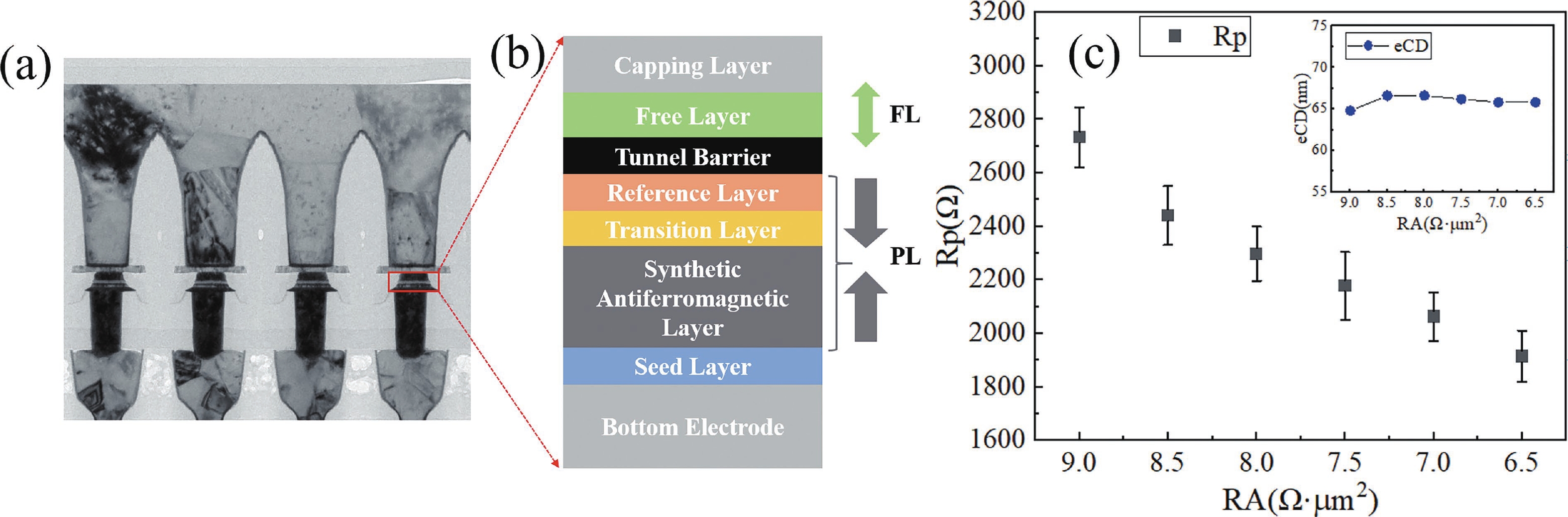
| [1] |
|
| [2] |
Myers E B, Ralph D C, Katine J A, et al. Current-induced switching of domains in magnetic multilayer devices. Science, 1999, 285(5429), 867 doi: 10.1126/science.285.5429.867 |
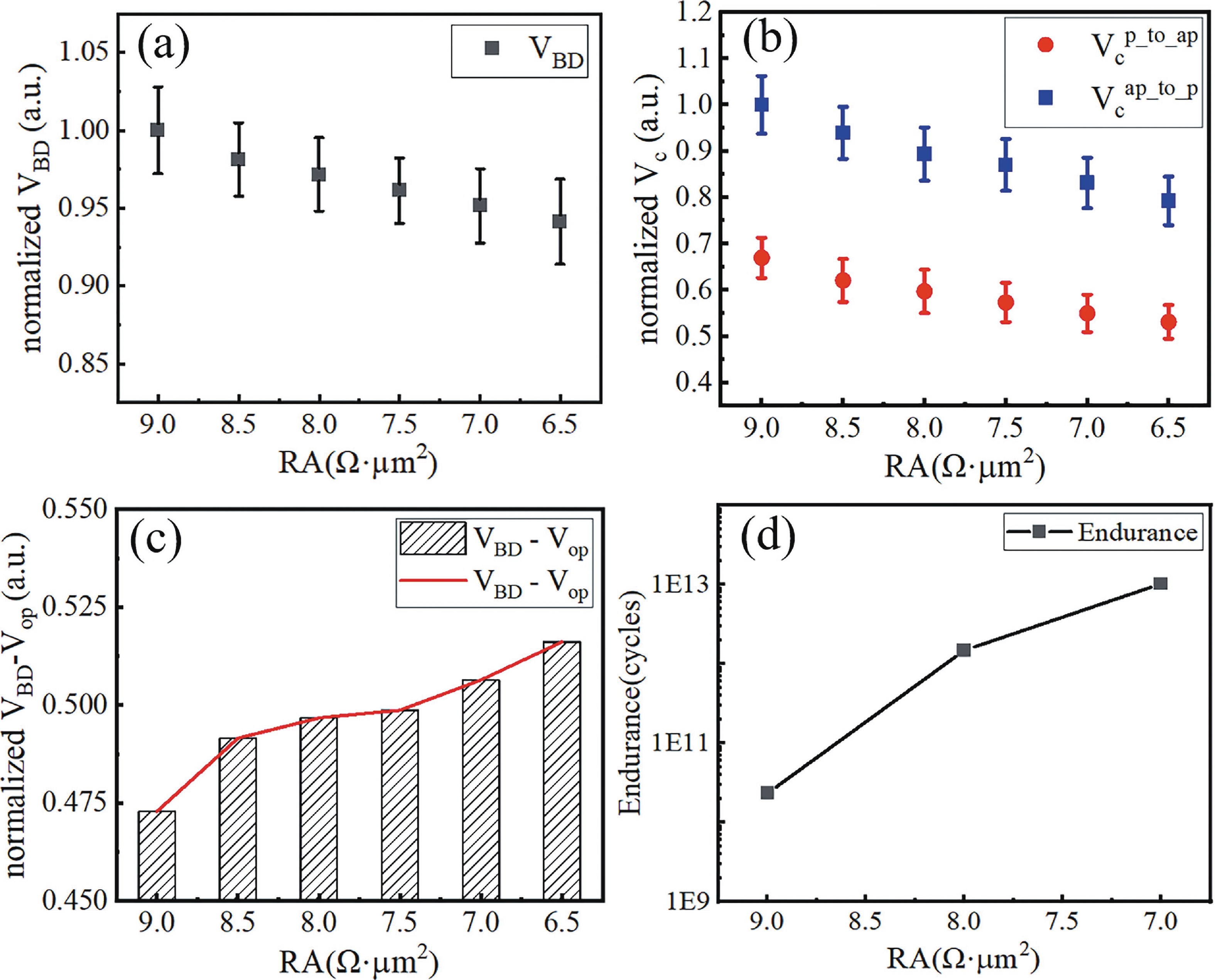
| [3] |
Ikegawa S, Mancoff F B, Janesky J, et al. Magnetoresistive random access memory: Present and future. IEEE Trans Electron Devices, 2020, 67(4), 1407 doi: 10.1109/TED.2020.2965403 |
| [4] |
Lee Y K, Song Y, Kim J, et al. Embedded STT-MRAM in 28-nm FDSOI logic process for industrial MCU/IoT application. 2018 IEEE Symposium on VLSI Technology, 2018, 181 doi: 10.1109/VLSIT.2018.8510623 |
| [5] |
Gallagher W J, Chien E, Chiang T W, et al. 22nm STT-MRAM for reflow and automotive uses with high yield, reliability, and magnetic immunity and with performance and shielding options. 2019 IEEE International Electron Devices Meeting (IEDM), 2019, 2.7.1 doi: 10.1109/IEDM19573.2019.8993469 |
| [6] |
Sato H, Honjo H, Watanabe T, et al. 14ns write speed 128Mb density Embedded STT-MRAM with endurance >10 10 and 10yrs retention@85°C using novel low damage MTJ integration process. 2018 IEEE International Electron Devices Meeting (IEDM), 2018, 27.2.1 doi: 10.1109/IEDM.2018.8614606 |
| [7] |
Endoh T, Honjo H. A recent progress of spintronics devices for integrated circuit applications. J Low Power Electron Appl, 2018, 8(4), 44 doi: 10.3390/jlpea8040044 |
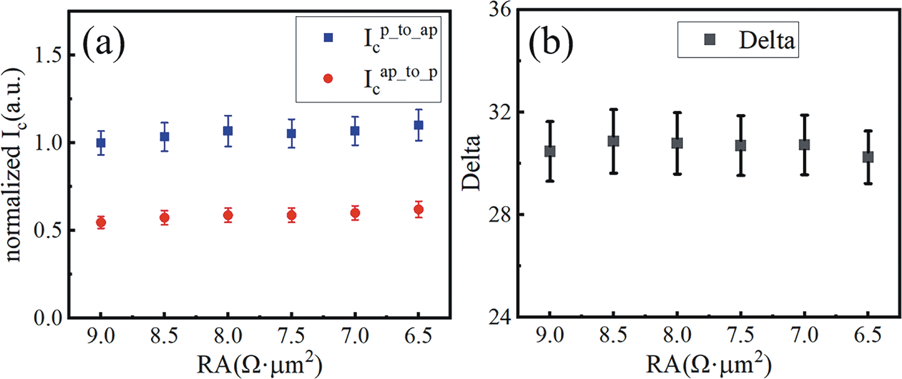
| [8] |
Song Y J, Lee J H, Han S H, et al. Demonstration of highly manufacturable STT-MRAM embedded in 28nm logic. 2018 IEEE International Electron Devices Meeting (IEDM), 2018, 18.2.1 doi: 10.1109/IEDM.2018.8614635 |
| [9] |
Alzate J G, Arslan U, Bai P, et al. 2 MB array-level demonstration of STT-MRAM process and performance towards L4 cache applications. 2019 IEEE International Electron Devices Meeting (IEDM), 2019, 2.4.1 doi: 10.1109/IEDM19573.2019.8993474 |
| [10] |
Lee K, Chao R, Yamane K, et al. 22-nm FD-SOI embedded MRAM technology for low-power automotive-grade-l MCU applications. 2018 IEEE International Electron Devices Meeting (IEDM), 2018, 27.1.1 doi: 10.1109/IEDM.2018.8614566 |
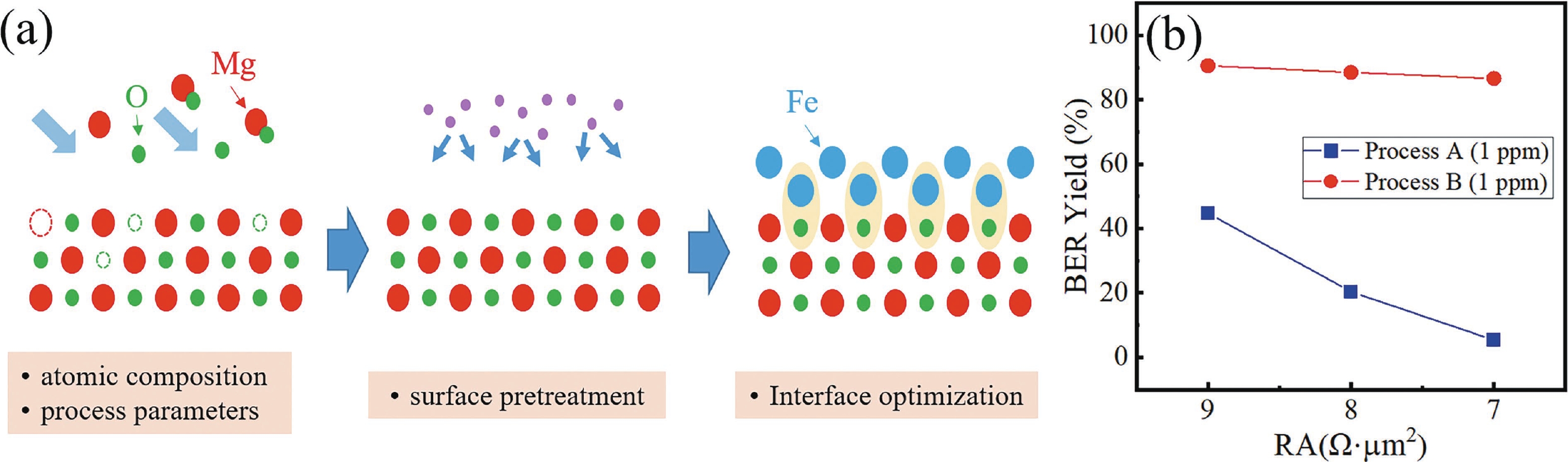
| [11] |
Golonzka O, Alzate J G, Arslan U, et al. MRAM as embedded non-volatile memory solution for 22FFL FinFET technology. 2018 IEEE International Electron Devices Meeting (IEDM), 2018, 18.1.1 doi: 10.1109/IEDM.2018.8614620 |
| [12] |
Chih Y D, Chou C C, Shih Y C, et al. Design challenges and solutions of emerging nonvolatile memory for embedded applications. 2021 IEEE International Electron Devices Meeting (IEDM), 2.4.1
|
| [13] |
Ikeda S, Miura K, Yamamoto H, et al. A perpendicular-anisotropy CoFeB−MgO magnetic tunnel junction. Nat Mater, 2010, 9, 721 doi: 10.1038/nmat2804 |
| [14] |
Sato H, Yamanouchi M, Ikeda S, et al. Perpendicular-anisotropy CoFeB-MgO magnetic tunnel junctions with a MgO/CoFeB/Ta/CoFeB/MgO recording structure. Appl Phys Lett, 2012, 101(2), 022414 doi: 10.1063/1.4736727 |
| [15] |
Nishioka K, Honjo H, Ikeda S, et al. Novel Quad interface MTJ technology and its first demonstration with high thermal stability and switching efficiency for STT-MRAM beyond 2X nm. 2019 Symposium on VLSI Technology, 2019, T120 doi: 10.23919/VLSIT.2019.8776499 |
| [16] |
Sato H, Enobio E C I, Yamanouchi M, et al. Properties of magnetic tunnel junctions with a MgO/CoFeB/Ta/CoFeB/MgO recording structure down to junction diameter of 11 nm. Appl Phys Lett, 2014, 105(6), 062403 doi: 10.1063/1.4892924 |
| [17] |
Naganuma H, Miura S, Honjo H, et al. Advanced 18 nm Quad-MTJ technology overcomes dilemma of retention and endurance under scaling beyond 2X nm. 2021 Symposium on VLSI Technology, 2021, 1
|
| [18] |
Park C, Lee H, Ching C, et al. Low RA magnetic tunnel junction arrays in conjunction with low switching current and high breakdown voltage for STT-MRAM at 10 nm and beyond. 2018 IEEE Symposium on VLSI Technology, 2018, 185 doi: 10.1109/VLSIT.2018.8510653 |
| [19] |
Wang Y, Cai H, de Barros Naviner L A, et al. Compact model of dielectric breakdown in spin-transfer torque magnetic tunnel junction. IEEE Trans Electron Devices, 2016, 63(4), 1762 doi: 10.1109/TED.2016.2533438 |
| [20] |
Tezuka N, Oikawa S, Abe I, et al. Perpendicular magnetic tunnel junctions with low resistance-area product: High output voltage and bias dependence of magnetoresistance. IEEE Magn Lett, 2016, 7, 3104204 doi: 10.1109/LMAG.2016.2584582 |
| [21] |
Jan G, Thomas L, Le S, et al. Demonstration of ultra-low voltage and ultra low power STT-MRAM designed for compatibility with 0x node embedded LLC applications. 2018 IEEE Symposium on VLSI Technology, 2018, 65 doi: 10.1109/VLSIT.2018.8510672 |
| [22] |
Oliver B, Tuttle G, He Q, et al. Two breakdown mechanisms in ultrathin alumina barrier magnetic tunnel junctions. J Appl Phys, 2004, 95(3), 1315 doi: 10.1063/1.1636255 |
| [23] |
Dimitrov D V, Gao Z, Wang X B, et al. Dielectric breakdown of MgO magnetic tunnel junctions. Appl Phys Lett, 2009, 94(12), 123110 doi: 10.1063/1.3109792 |
| [24] |
Su J Z, Zhu Q H, Hou Y R, et al. Modeling of endurance degradation and hard breakdown for MRAM-OTP demonstration. IEEE Electron Device Lett, 2025, 46(8), 1333 doi: 10.1109/LED.2025.3581530 |
| [25] |
Brinkman W F, Dynes R C, Rowell J M. Tunneling conductance of asymmetrical barriers. J Appl Phys, 1970, 41(5), 1915 doi: 10.1063/1.1659141 |
| [26] |
Naik V B, Yamane K, Lee T Y, et al. JEDEC-qualified highly reliable 22nm FD-SOI embedded MRAM for low-power industrial-grade, and extended performance towards automotive-grade-1 applications. 2020 IEEE International Electron Devices Meeting (IEDM), 2020, 11.3.1 doi: 10.1109/IEDM13553.2020.9371935 |
| [27] |
Khvalkovskiy A V, Apalkov D, Watts S, et al. Basic principles of STT-MRAM cell operation in memory arrays. J Phys D: Appl Phys, 2013, 46(7), 074001 doi: 10.1088/0022-3727/46/7/074001 |
| [28] |
Zeng D G, Meng F T, Chen R F, et al. Achieving over 95% yield of sub-1 ppm BER with retention over 10 years at 125 °C and endurance of 1 × 10 12 cycles towards automotive non-volatile RAM applications. J Semicond, 2025, 46(3), 032301 doi: 10.1088/1674-4926/24090037 |
| [29] |
Lee T Y, Lee J M, Kim M K, et al. World-most energy-efficient MRAM technology for non-volatile RAM applications. 2022 International Electron Devices Meeting (IEDM), 2022, 10.7.1 doi: 10.1109/IEDM45625.2022.10019430 |
| [30] |
Wang Y, Chen Y H, Chih Y D, et al. High-speed embedded memory for AI and high-performance compute. 2023 International Electron Devices Meeting (IEDM), 2023, 1 doi: 10.1109/IEDM45741.2023.10413818 |
| [31] |
Oh J, Park J, Suh K, et al. 14nm FinFET node embedded MRAM technology for automotive non-volatile RAM applications with endurance over 1E12-cycles. 2024 IEEE Symposium on VLSI Technology and Circuits (VLSI Technology and Circuits), 2024, 1 doi: 10.1109/VLSITechnologyandCir46783.2024.10631315 |
| [32] |
Zeng Z M, Khalili Amiri P, Rowlands G, et al. Effect of resistance-area product on spin-transfer switching in MgO-based magnetic tunnel junction memory cells. Appl Phys Lett, 2011, 98(7), 072512 doi: 10.1063/1.3556615 |
| [33] |
Mihajlović G, Smith N, Santos T, et al. Origin of the resistance-area-product dependence of spin-transfer-torque switching in perpendicular magnetic random-access memory cells. Phys Rev Applied, 2020, 13(2), 024004 doi: 10.1103/PhysRevApplied.13.024004 |
| [34] |
Hou Y R, Du H R, Su J Z, et al. A 40nm 4Mb high-reliability STT-MRAM achieving 18ns write-time and 94.9% wafer-level-die-yield across-55°C-to-125°C. 2025 IEEE Custom Integrated Circuits Conference (CICC), 2025, 1 doi: 10.1109/CICC63670.2025.10983180 |


 Kunkun Li got his BS in 2013 and PhD degree in 2018 at Institute of Physics Chinese Academy of Sciences. In 2021, he joined Hikstor as engineer. His research interest focuses on Semiconductor, Flash memory and MRAM.
 Shikun He got his BS in 2005 and PhD degree in 2012 at Institute of Physics Chinese Academy of Sciences. In 2016, he joined Hikstor as principle engineer and promoted to product R & D leader. His research interest focuses on spintronics materials, devices and systems.
 DownLoad: