| [1] |
Chen J, Sun M Y, Wang Z H, et al. Performance limits and advancements in single 2D transition metal dichalcogenide transistor. Nanomicro Lett, 2024, 16(1), 264 doi: 10.1007/s40820-024-01461-x |
| [2] |
Wu R X, Tao Q Y, Li J, et al. Bilayer tungsten diselenide transistors with on-state currents exceeding 1.5 milliamperes per micrometre. Nat Electron, 2022, 5(8), 497 doi: 10.1038/s41928-022-00800-3 |
| [3] |
Park J H, Fathipour S, Kwak I, et al. Atomic layer deposition of Al 2O 3 on WSe 2 functionalized by titanyl phthalocyanine. ACS Nano, 2016, 10(7), 6888 doi: 10.1021/acsnano.6b02648 |
| [4] |
Wang Y, Chhowalla M. Making clean electrical contacts on 2D transition metal dichalcogenides. Nat Rev Phys, 2022, 4, 101
|
| [5] |
Han H C, Zhang B Q, Zhang Z H, et al. Light-triggered anti-ambipolar transistor based on an in-plane lateral homojunction. Nano Lett, 2024, 24(28), 8602 doi: 10.1021/acs.nanolett.4c01679 |
| [6] |
Lin Y T, Hsu C H, Chou A S, et al. Antimony-platinum modulated contact enabling majority carrier polarity selection on a monolayer tungsten diselenide channel. Nano Lett, 2024, 24(29), 8880 doi: 10.1021/acs.nanolett.4c01436 |
| [7] |
Ghosh S, Sadaf M U K, Graves A R, et al. High-performance p-type bilayer WSe 2 field effect transistors by nitric oxide doping. Nat Commun, 2025, 16, 5649 doi: 10.1038/s41467-025-59684-4 |
| [8] |
Wang Y, Kim J C, Li Y, et al. P-type electrical contacts for 2D transition-metal dichalcogenides. Nature, 2022, 610, 61 doi: 10.1038/s41586-022-05134-w |
| [9] |
Das M, Sen D, Sakib N U, et al. High-performance p-type field-effect transistors using substitutional doping and thickness control of two-dimensional materials. Nat Electron, 2025, 8, 24 doi: 10.1038/s41928-024-01265-2 |
| [10] |
Zhao S W, Huang J Q, Crépel V, et al. Fractional quantum Hall phases in high-mobility n-type molybdenum disulfide transistors. Nat Electron, 2024, 7, 1117 doi: 10.1038/s41928-024-01274-1 |
| [11] |
|
| [12] |
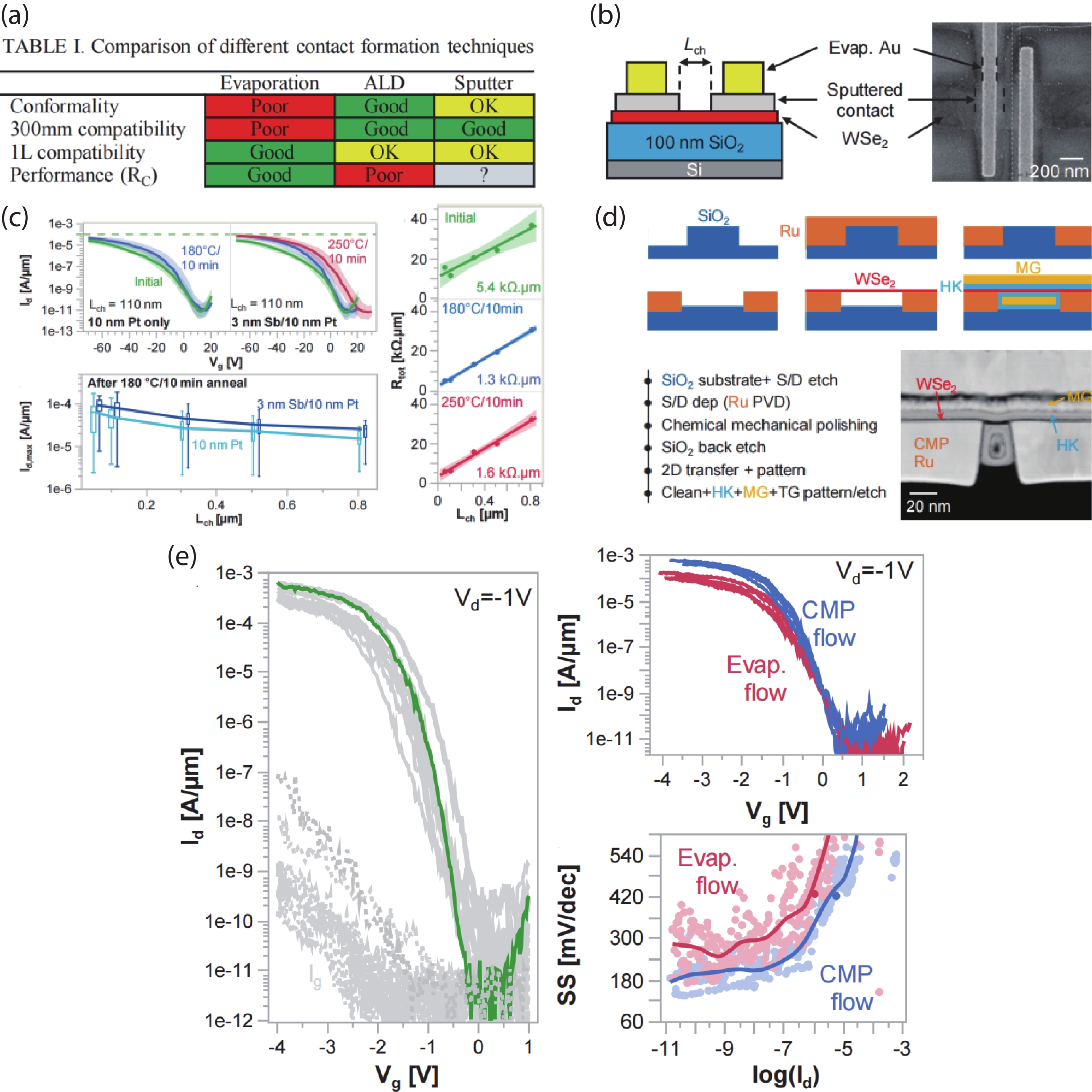
Jaikissoon M, Buragohain P, Mortelmans W, et al. Record PMOS WSe 2 GAA performance using contact planarization, and systematic exploration of manufacturable, high-yield contacts. Symp VLSI Technology, 2025 doi: 10.23919/VLSITechnologyandCir65189.2025.11075202 |


 Haoyu Peng is an undergraduate student at the University of the Chinese Academy of Sciences. He recently completed a research internship in the experimental group of Jiangbin Wu at the Institute of Semiconductors, Chinese Academy of Sciences.
 Ping-Heng Tan is a professor at the Institute of Semiconductors, Chinese Academy of Sciences. He obtained his B.S. degree in Physics from Peking University in 1996 and his Ph.D. from the Institute of Semiconductors, Chinese Academy of Sciences in 2001. From 2001 to 2003, he worked as a postdoctoral research associate at the Walter Schottky Institute of the Technical University of Munich. He was a K. C. Wong Royal Society Fellow at the University of Cambridge from 2006 to 2007. His current research focuses on two-dimensional layered materials, carbon nanomaterials, topological insulators, and other novel low-dimensional semiconductor optoelectronic materials. In 2012, he received the National Science Fund for Distinguished Young Scholars.
 Jiangbin Wu has been a professor at the Institute of Semiconductors, Chinese Academy of Sciences since 2023. He received his Ph.D. from the Institute of Semiconductors, Chinese Academy of Sciences in 2017. Then he worked as a postdoctoral research associate at the University of Southern California until 2023. His research interests include exploring the optoelectronic properties of new low-dimensional materials, controlling their properties, and building high-performance semiconductor devices based on these materials. His publications have received a total of more than 11 000 citations with a h index of 36 as of August 2025.
 DownLoad: