


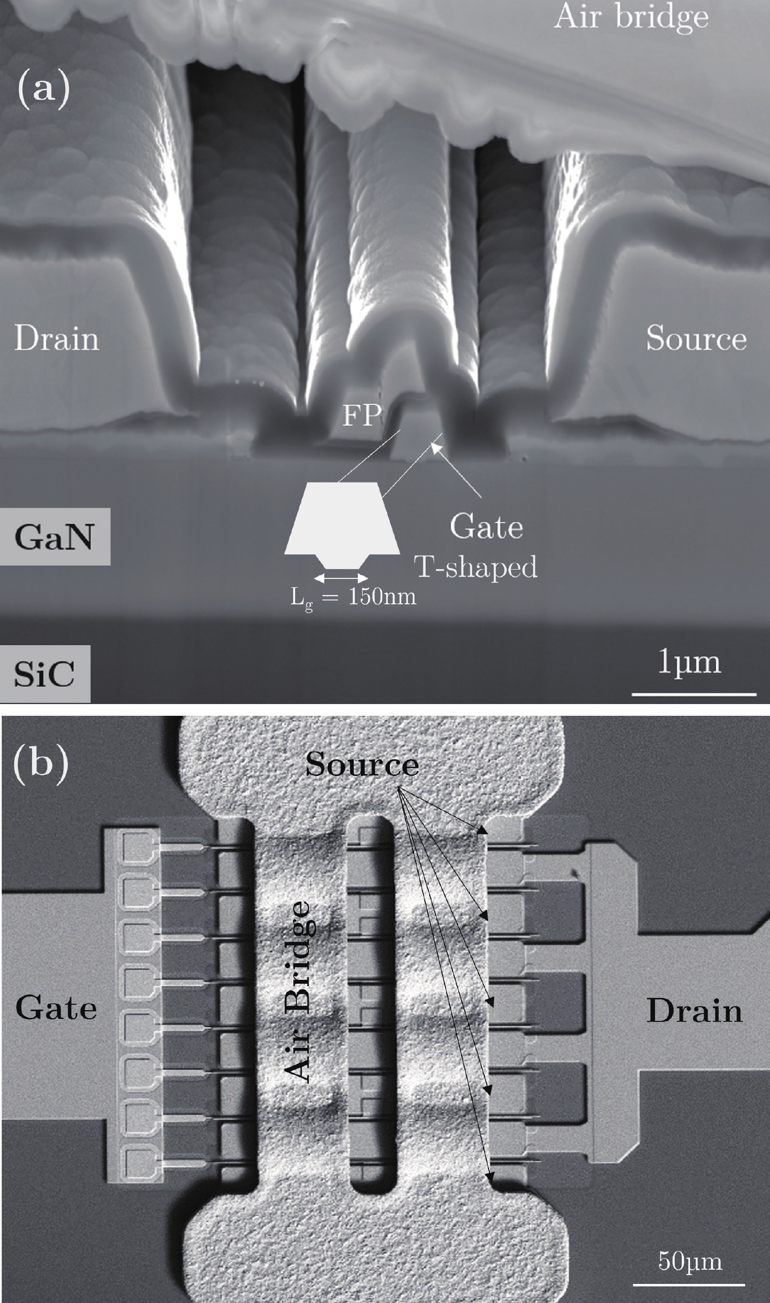
Fig. 1.
(a) Cross-sectional SEM image of a single gate finger of the DUT. (b) Top-view image of the complete device, showing the gate, source, and drain access regions.
ARTICLES
El Mehdi Meknassi1, Niemat Moultif1, Sebastien Duguay1, Benoit Lambert2, Gabriel Bertao2 and Olivier Latry1,
Corresponding author: Olivier Latry, olivier.latry@univ-rouen.fr
Abstract: This work focuses on the early-life drift mechanisms in 150 nm AlGaN/GaN HEMTs on SiC under RF-HTOL stress at 9 GHz and 130 °C. Electrical measurements during the first hours of stress reveal significant shifts in threshold voltage, transconductance, and drain lag, indicating the activation of deep traps located in the buffer. A transient increase in gate leakage current is also observed under reverse gate bias, suggesting additional trapping or conduction paths at the AlGaN/SiN or cap/passivation interface. These electrical instabilities coincide with a progressive degradation of RF performance, notably in gain and power-added efficiency. Electroluminescence measurements further support the presence of electrically active defects, with distinct spatial patterns depending on the bias configuration.
Keywords: RF-HTOL, GaN HEMTs, early-life, traps
| [1] |
Lu H, Zhang M, Yang L, et al. A review of GaN RF devices and power amplifiers for 5G communication applications. Fundam Res, 2025, 5(1): 315 doi: 10.1016/j.fmre.2023.11.005
|
| [2] |
Marcon D, Kang X, Viaene J, et al. GaN-based HEMTs tested under high temperature storage test. Microelectron Reliab, 2011, 51(9/10/11): 1717 doi: 10.1016/j.microrel.2011.06.062
|
| [3] |
Moultif N, Latry O, Ndiaye M, et al. S-band pulsed-RF operating life test on AlGaN/GaN HEMT devices for radar application. Microelectron Reliab, 2019, 100: 113434 doi: 10.1016/j.microrel.2019.113434
|
| [4] |
Tayyab M F, Silvestri M, Bernardoni M, et al. Dynamic high temperature operating life test methodology for long-term switching reliability of GaN power devices. Microelectron Reliab, 2022, 138: 114613 doi: 10.1016/j.microrel.2022.114613
|
| [5] |
De Santi C, Meneghini M, Meneghesso G, et al. Review of dynamic effects and reliability of depletion and enhancement GaN HEMTs for power switching applications. IET Power Electron, 2018, 11(4): 668 doi: 10.1049/iet-pel.2017.0403
|
| [6] |
Meneghini M, De Santi C, Abid I, et al. GaN-based power devices: Physics, reliability, and perspectives. J Appl Phys, 2021, 130(18): 181101 doi: 10.1063/5.0061354
|
| [7] |
Joh J, del Alamo J A. Critical voltage for electrical degradation of GaN high-electron mobility transistors. IEEE Electron Device Lett, 2008, 29(4): 287 doi: 10.1109/LED.2008.917815
|
| [8] |
Meneghini M, Stocco A, Silvestri R, et al. Degradation of AlGaN/GaN high electron mobility transistors related to hot electrons. Appl Phys Lett, 2012, 100(23): 233508 doi: 10.1063/1.4723848
|
| [9] |
Cheney D J, Douglas E A, Liu L, et al. Reliability studies of AlGaN/GaN high electron mobility transistors. Semicond Sci Technol, 2013, 28(7): 074019 doi: 10.1088/0268-1242/28/7/074019
|
| [10] |
Douglas E A, Pearton S J, Poling B, et al. Effect of drain bias on degradation of AlGaN∕GaN high electron mobility transistors under X-band operation. Electrochem Solid-State Lett, 2011, 14(11): H464 doi: 10.1149/2.019111esl
|
| [11] |
Temcamani F, Fonder J B, Latry O, et al. Electrical and physical analysis of thermal degradations of AlGaN/GaN HEMT under radar-type operating life. IEEE Trans Microw Theory Tech, 2016, 64(3): 756 doi: 10.1109/tmtt.2016.2519342
|
| [12] |
Xu L L, Guo H, Wang S, et al. Impedance-dependent degradation in GaN HEMTs under high-voltage RF stress: Electro-thermal and trap mechanisms. Appl Phys Lett, 2025, 127(3): 032103 doi: 10.1063/5.0271954
|
| [13] |
Bisi D, Chini A, Soci F, et al. Hot-electron degradation of AlGaN/GaN high-electron mobility transistors during RF operation: Correlation with GaN buffer design. IEEE Electron Device Lett, 2015, 36(10): 1011 doi: 10.1109/LED.2015.2474116
|
| [14] |
Wang Y S, Zeng C, Lai P. Degradation in AlGaN/GaN HEMT under high temperature reverse bias stress. 2014 10th International Conference on Reliability, Maintainability and Safety (ICRMS), 2015: 165
|
| [15] |
Pilati M, Buffolo M, Rampazzo F, et al. Impact of high-temperature operating lifetime tests on the stability of 0.15 μm AlGaN/GaN HEMTs: A temperature-dependent analysis. Microelectron Reliab, 2023, 150: 115131 doi: 10.1016/j.microrel.2023.115131
|
| [16] |
Magnier F, Lambert B, Chang C, et al. Investigation of trap induced power drift on 0.15 μm GaN technology after aging tests. Microelectron Reliab, 2019, 100/101: 113358 doi: 10.1016/j.microrel.2019.06.050
|
| [17] |
Pallaro T, Dubois T, De Matos M, et al. DC and RF aging test of AlGaN/GaN HEMT technology on SiC substrate. Microelectron Reliab, 2025, 170: 115772 doi: 10.1016/j.microrel.2025.115772
|
| [18] |
Latry O, Joubert E, Neveu T, et al. Temperature estimation of high-electron mobility transistors AlGaN/GaN. 2018 19th IEEE Mediterranean Electrotechnical Conference (MELECON), 2018: 265
|
| [19] |
Latry O, Divay A, Fadil D, et al. Extraction of physical Schottky parameters using the Lambert function in Ni/AlGaN/GaN HEMT devices with defined conduction phenomena. J Semicond, 2017, 38(1): 014007 doi: 10.1088/1674-4926/38/1/014007
|
| [20] |
Meneghesso G, Verzellesi G, Danesin F, et al. Reliability of GaN high-electron-mobility transistors: State of the art and perspectives. IEEE Trans Device Mater Relib, 2008, 8(2): 332 doi: 10.1109/TDMR.2008.923743
|
| [21] |
Marcon D, Meneghesso G, Wu T L, et al. Reliability analysis of permanent degradations on AlGaN/GaN HEMTs. IEEE Trans Electron Devices, 2013, 60(10): 3132 doi: 10.1109/TED.2013.2273216
|
| [22] |
Arulkumaran S, Egawa T, Ishikawa H. Studies on the influences of i-GaN, n-GaN, p-GaN and InGaN cap layers in AlGaN/GaN high-electron-mobility transistors. Jpn J Appl Phys, 2005, 44(5R): 2953 doi: 10.1143/JJAP.44.2953
|
| [23] |
Nie Z R, Wang K, Liu X Y, et al. Effect of GaN cap thickness on the DC performance of AlGaN/GaN HEMTs. Micromachines, 2024, 15(5): 571 doi: 10.3390/mi15050571
|
| [24] |
Zhang S, Wei K, Zhang Y C, et al. Well-suppressed interface states and improved transport properties of AlGaN/GaN MIS-HEMTs with PEALD SiN gate dielectric. Vacuum, 2021, 191: 110359 doi: 10.1016/j.vacuum.2021.110359
|
| [25] |
Charles M, Baines Y, Bouis R, et al. The characterization and optimization of GaN cap layers and SiN cap layers on AlGaN/GaN HEMT structures grown on 200 mm GaN on silicon. Phys Status Solidi B, 2018, 255(5): 1700406 doi: 10.1002/pssb.201700406
|
| [26] |
Kaushik J K, Balakrishnan V R, Mongia D, et al. Investigation of surface related leakage current in AlGaN/GaN high electron mobility transistors. Thin Solid Films, 2016, 612: 147 doi: 10.1016/j.tsf.2016.06.003
|
| [27] |
Jabbari I, Baira M, Maaref H, et al. Evidence of Poole-Frenkel and Fowler-Nordheim tunneling transport mechanisms in leakage current of (Pd/Au)/Al0.22Ga0.78N/GaN heterostructures. Solid State Commun, 2020, 314/315: 113920 doi: 10.1016/j.ssc.2020.113920
|
| [28] |
Hodges C, Killat N, Kaun S W, et al. Optical investigation of degradation mechanisms in AlGaN/GaN high electron mobility transistors: Generation of non-radiative recombination centers. Appl Phys Lett, 2012, 100(11): 112106 doi: 10.1063/1.3693427
|
| [29] |
Moultif N, Divay A, Joubert E, et al. Localizing and analyzing defects in AlGaN/GaN HEMT using photon emission spectral signatures. Eng Fail Anal, 2017, 81: 69 doi: 10.1016/j.engfailanal.2017.07.014
|
| [30] |
Latrach S, Frayssinet E, Defrance N, et al. Trap states analysis in AlGaN/AlN/GaN and InAlN/AlN/GaN high electron mobility transistors. Curr Appl Phys, 2017, 17(12): 1601 doi: 10.1016/j.cap.2017.09.003
|
| [31] |
Matsubara M, Bellotti E. A first-principles study of carbon-related energy levels in GaN. I. Complexes formed by substitutional/interstitial carbons and gallium/nitrogen vacancies. J Appl Phys, 2017, 121(19): 195701 doi: 10.1063/1.4983452
|
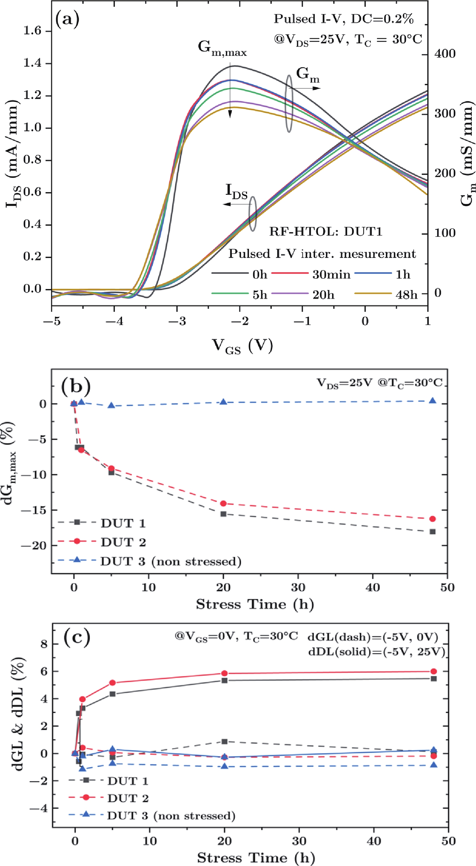
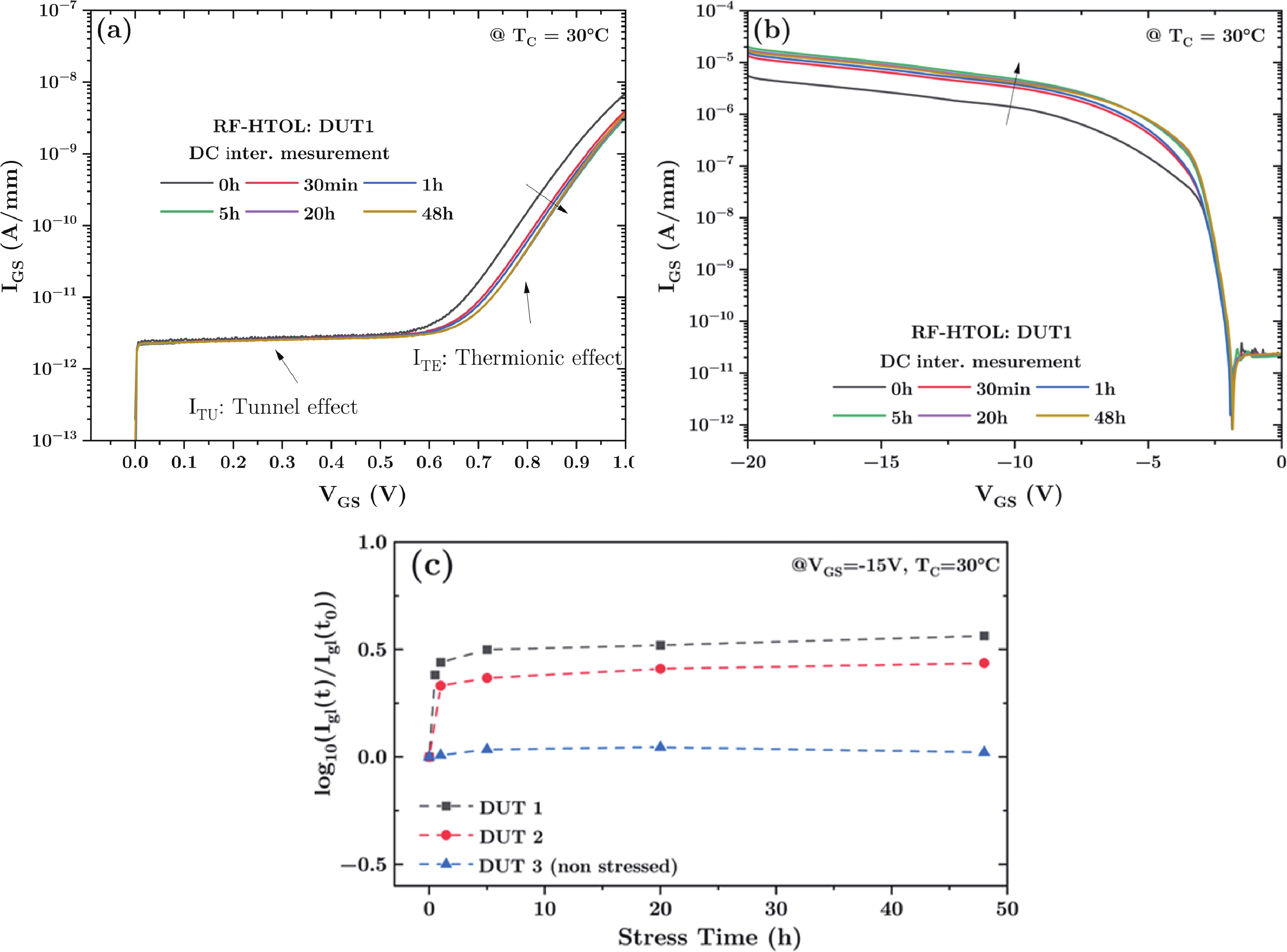
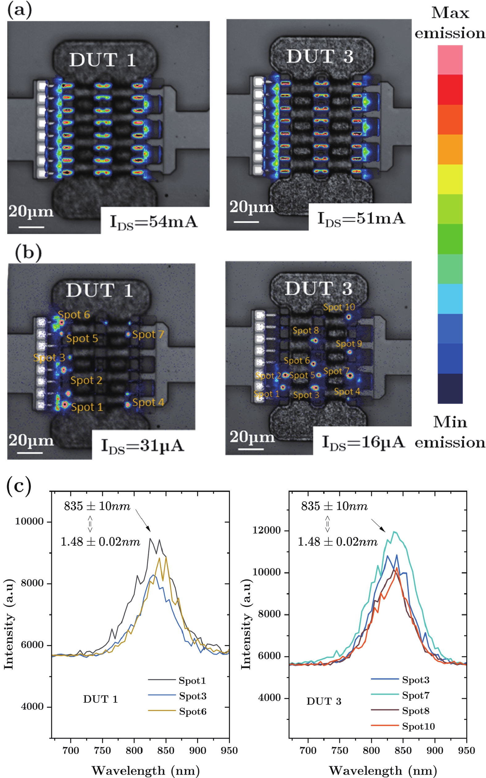
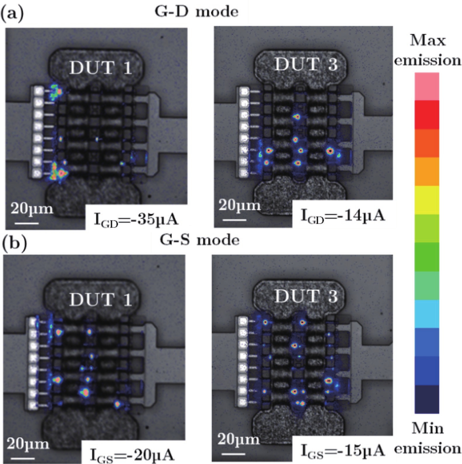
Table 1. Summary of RF-HTOL stress conditions.
| Stress conditions |
f = 9 GHz, Pin = 29 dBm, VDSq = 25 V, IDSq = 200 mA/mm, Tb = 130 °C |
|||
| Device | DUT 1 | DUT 2 | DUT 3 (ref.) | |
| VGSq @30 °C | −2.21 V | −2.16 V | −2.23 V | |
| VGSq @130 °C | −2.41 V | −2.35 V | ||
| Intermediate measurement |
t0, 30 min, 1 h, 5 h, 20 h, 48 h |
t0, 1 h, 5 h, 20 h, 48 h |
t0, 1 h, 5 h, 20 h, 48 h |
|
 DownLoad: CSV
Table 2. Summary of Schottky diode parameters extracted from forward-bias measurements under RF-HTOL stress for DUTs 1 and 2: average values of tunneling current (ITU), Schottky barrier height (ΦB), and ideality factor (n), and their relative variations during stress.
| Stress conditions | Forward-bias diode (DUTs 1 & 2) | ||
| ITU | ΦB | n | |
| Average values | 3 pA | 0.96 eV | 1.66 |
| RF-HTOL variations | <1% | <2%−3% | <2% |
DownLoad: CSV
| [1] |
Lu H, Zhang M, Yang L, et al. A review of GaN RF devices and power amplifiers for 5G communication applications. Fundam Res, 2025, 5(1): 315 doi: 10.1016/j.fmre.2023.11.005
|
| [2] |
Marcon D, Kang X, Viaene J, et al. GaN-based HEMTs tested under high temperature storage test. Microelectron Reliab, 2011, 51(9/10/11): 1717 doi: 10.1016/j.microrel.2011.06.062
|
| [3] |
Moultif N, Latry O, Ndiaye M, et al. S-band pulsed-RF operating life test on AlGaN/GaN HEMT devices for radar application. Microelectron Reliab, 2019, 100: 113434 doi: 10.1016/j.microrel.2019.113434
|
| [4] |
Tayyab M F, Silvestri M, Bernardoni M, et al. Dynamic high temperature operating life test methodology for long-term switching reliability of GaN power devices. Microelectron Reliab, 2022, 138: 114613 doi: 10.1016/j.microrel.2022.114613
|
| [5] |
De Santi C, Meneghini M, Meneghesso G, et al. Review of dynamic effects and reliability of depletion and enhancement GaN HEMTs for power switching applications. IET Power Electron, 2018, 11(4): 668 doi: 10.1049/iet-pel.2017.0403
|
| [6] |
Meneghini M, De Santi C, Abid I, et al. GaN-based power devices: Physics, reliability, and perspectives. J Appl Phys, 2021, 130(18): 181101 doi: 10.1063/5.0061354
|
| [7] |
Joh J, del Alamo J A. Critical voltage for electrical degradation of GaN high-electron mobility transistors. IEEE Electron Device Lett, 2008, 29(4): 287 doi: 10.1109/LED.2008.917815
|
| [8] |
Meneghini M, Stocco A, Silvestri R, et al. Degradation of AlGaN/GaN high electron mobility transistors related to hot electrons. Appl Phys Lett, 2012, 100(23): 233508 doi: 10.1063/1.4723848
|
| [9] |
Cheney D J, Douglas E A, Liu L, et al. Reliability studies of AlGaN/GaN high electron mobility transistors. Semicond Sci Technol, 2013, 28(7): 074019 doi: 10.1088/0268-1242/28/7/074019
|
| [10] |
Douglas E A, Pearton S J, Poling B, et al. Effect of drain bias on degradation of AlGaN∕GaN high electron mobility transistors under X-band operation. Electrochem Solid-State Lett, 2011, 14(11): H464 doi: 10.1149/2.019111esl
|
| [11] |
Temcamani F, Fonder J B, Latry O, et al. Electrical and physical analysis of thermal degradations of AlGaN/GaN HEMT under radar-type operating life. IEEE Trans Microw Theory Tech, 2016, 64(3): 756 doi: 10.1109/tmtt.2016.2519342
|
| [12] |
Xu L L, Guo H, Wang S, et al. Impedance-dependent degradation in GaN HEMTs under high-voltage RF stress: Electro-thermal and trap mechanisms. Appl Phys Lett, 2025, 127(3): 032103 doi: 10.1063/5.0271954
|
| [13] |
Bisi D, Chini A, Soci F, et al. Hot-electron degradation of AlGaN/GaN high-electron mobility transistors during RF operation: Correlation with GaN buffer design. IEEE Electron Device Lett, 2015, 36(10): 1011 doi: 10.1109/LED.2015.2474116
|
| [14] |
Wang Y S, Zeng C, Lai P. Degradation in AlGaN/GaN HEMT under high temperature reverse bias stress. 2014 10th International Conference on Reliability, Maintainability and Safety (ICRMS), 2015: 165
|
| [15] |
Pilati M, Buffolo M, Rampazzo F, et al. Impact of high-temperature operating lifetime tests on the stability of 0.15 μm AlGaN/GaN HEMTs: A temperature-dependent analysis. Microelectron Reliab, 2023, 150: 115131 doi: 10.1016/j.microrel.2023.115131
|
| [16] |
Magnier F, Lambert B, Chang C, et al. Investigation of trap induced power drift on 0.15 μm GaN technology after aging tests. Microelectron Reliab, 2019, 100/101: 113358 doi: 10.1016/j.microrel.2019.06.050
|
| [17] |
Pallaro T, Dubois T, De Matos M, et al. DC and RF aging test of AlGaN/GaN HEMT technology on SiC substrate. Microelectron Reliab, 2025, 170: 115772 doi: 10.1016/j.microrel.2025.115772
|
| [18] |
Latry O, Joubert E, Neveu T, et al. Temperature estimation of high-electron mobility transistors AlGaN/GaN. 2018 19th IEEE Mediterranean Electrotechnical Conference (MELECON), 2018: 265
|
| [19] |
Latry O, Divay A, Fadil D, et al. Extraction of physical Schottky parameters using the Lambert function in Ni/AlGaN/GaN HEMT devices with defined conduction phenomena. J Semicond, 2017, 38(1): 014007 doi: 10.1088/1674-4926/38/1/014007
|
| [20] |
Meneghesso G, Verzellesi G, Danesin F, et al. Reliability of GaN high-electron-mobility transistors: State of the art and perspectives. IEEE Trans Device Mater Relib, 2008, 8(2): 332 doi: 10.1109/TDMR.2008.923743
|
| [21] |
Marcon D, Meneghesso G, Wu T L, et al. Reliability analysis of permanent degradations on AlGaN/GaN HEMTs. IEEE Trans Electron Devices, 2013, 60(10): 3132 doi: 10.1109/TED.2013.2273216
|
| [22] |
Arulkumaran S, Egawa T, Ishikawa H. Studies on the influences of i-GaN, n-GaN, p-GaN and InGaN cap layers in AlGaN/GaN high-electron-mobility transistors. Jpn J Appl Phys, 2005, 44(5R): 2953 doi: 10.1143/JJAP.44.2953
|
| [23] |
Nie Z R, Wang K, Liu X Y, et al. Effect of GaN cap thickness on the DC performance of AlGaN/GaN HEMTs. Micromachines, 2024, 15(5): 571 doi: 10.3390/mi15050571
|
| [24] |
Zhang S, Wei K, Zhang Y C, et al. Well-suppressed interface states and improved transport properties of AlGaN/GaN MIS-HEMTs with PEALD SiN gate dielectric. Vacuum, 2021, 191: 110359 doi: 10.1016/j.vacuum.2021.110359
|
| [25] |
Charles M, Baines Y, Bouis R, et al. The characterization and optimization of GaN cap layers and SiN cap layers on AlGaN/GaN HEMT structures grown on 200 mm GaN on silicon. Phys Status Solidi B, 2018, 255(5): 1700406 doi: 10.1002/pssb.201700406
|
| [26] |
Kaushik J K, Balakrishnan V R, Mongia D, et al. Investigation of surface related leakage current in AlGaN/GaN high electron mobility transistors. Thin Solid Films, 2016, 612: 147 doi: 10.1016/j.tsf.2016.06.003
|
| [27] |
Jabbari I, Baira M, Maaref H, et al. Evidence of Poole-Frenkel and Fowler-Nordheim tunneling transport mechanisms in leakage current of (Pd/Au)/Al0.22Ga0.78N/GaN heterostructures. Solid State Commun, 2020, 314/315: 113920 doi: 10.1016/j.ssc.2020.113920
|
| [28] |
Hodges C, Killat N, Kaun S W, et al. Optical investigation of degradation mechanisms in AlGaN/GaN high electron mobility transistors: Generation of non-radiative recombination centers. Appl Phys Lett, 2012, 100(11): 112106 doi: 10.1063/1.3693427
|
| [29] |
Moultif N, Divay A, Joubert E, et al. Localizing and analyzing defects in AlGaN/GaN HEMT using photon emission spectral signatures. Eng Fail Anal, 2017, 81: 69 doi: 10.1016/j.engfailanal.2017.07.014
|
| [30] |
Latrach S, Frayssinet E, Defrance N, et al. Trap states analysis in AlGaN/AlN/GaN and InAlN/AlN/GaN high electron mobility transistors. Curr Appl Phys, 2017, 17(12): 1601 doi: 10.1016/j.cap.2017.09.003
|
| [31] |
Matsubara M, Bellotti E. A first-principles study of carbon-related energy levels in GaN. I. Complexes formed by substitutional/interstitial carbons and gallium/nitrogen vacancies. J Appl Phys, 2017, 121(19): 195701 doi: 10.1063/1.4983452
|


Article views: 870 Times PDF downloads: 169 Times Cited by: 0 Times
Received: 25 August 2025 Revised: 07 January 2026 Online: Accepted Manuscript: 31 January 2026Uncorrected proof: 26 February 2026Published: 14 May 2026
| Citation: |
El Mehdi Meknassi, Niemat Moultif, Sebastien Duguay, Benoit Lambert, Gabriel Bertao, Olivier Latry. Investigation of trapping dynamics and defect evolution in 150 nm GaN-on-SiC HEMTs under early X-band RF stress[J]. Journal of Semiconductors, 2026, 47(5): 052502. doi: 10.1088/1674-4926/25080031
****
E M Meknassi, N Moultif, S Duguay, B Lambert, G Bertao, and O Latry, Investigation of trapping dynamics and defect evolution in 150 nm GaN-on-SiC HEMTs under early X-band RF stress[J]. J. Semicond., 2026, 47(5): 052502 doi: 10.1088/1674-4926/25080031

|
 El Mehdi Meknassi received a Master’s degree in Applied Physics and Physical Engineering in 2022. He recently obtained a Ph.D. degree in physics and microelectronics from University of Rouen Normandy in December 2025, where he carried out his research at the GPM Laboratory. He is currently a postdoctoral researcher. His research interests focus on the reliability of GaN-based RF devices, combining electrical characterization with advanced materials characterization techniques
 Niemat Moultif received an engineering degree in telecommunication systems and network engineering from ENSA of Tangier in 2013 and a Ph.D. degree in physics and reliability from the University of Rouen Normandy, France in 2017. She is currently an assistant professor at the GPM Laboratory of the University of Rouen Normandy. Her main research interests are reliability and characterization of high-power devices: RF GaN HEMT devices and SiC MOSFETs
 Sebastien Duguay is an assistant professor at the GPM laboratory, University of Rouen, in France which he joined in 2007. He is a specialist of atom probe tomography related to semiconductors. He graduated from INSA of Rennes (France), an engineering school, in 2002. He then joined the University of Strasbourg and the ICUBE laboratory to carry out his master and obtain his Ph.D. thesis in the field of microelectronics in 2006
 Olivier Latry received his Ph.D. in Electrical Engineering from the University of Normandy Rouen, France, in 1995. He is currently a Full Professor at GPM laboratory of the University of Rouen Normandy. His research focuses on microelectronic reliability, particularly in GaN power transistors. He teaches electronics and microwave engineering at the University Institute of Technology and radar systems at the Microwave and Radar Training Center (MRTC) in Normandy, France. As one of the founders of the MRTC, he was awarded the Research, Technology, and Innovation Prize by the Aerospace Normandy network in 2019 for his contributions to the aerospace, defense, and security industries
| [1] |
Lu H, Zhang M, Yang L, et al. A review of GaN RF devices and power amplifiers for 5G communication applications. Fundam Res, 2025, 5(1): 315 doi: 10.1016/j.fmre.2023.11.005
|
| [2] |
Marcon D, Kang X, Viaene J, et al. GaN-based HEMTs tested under high temperature storage test. Microelectron Reliab, 2011, 51(9/10/11): 1717 doi: 10.1016/j.microrel.2011.06.062
|
| [3] |
Moultif N, Latry O, Ndiaye M, et al. S-band pulsed-RF operating life test on AlGaN/GaN HEMT devices for radar application. Microelectron Reliab, 2019, 100: 113434 doi: 10.1016/j.microrel.2019.113434
|
| [4] |
Tayyab M F, Silvestri M, Bernardoni M, et al. Dynamic high temperature operating life test methodology for long-term switching reliability of GaN power devices. Microelectron Reliab, 2022, 138: 114613 doi: 10.1016/j.microrel.2022.114613
|
| [5] |
De Santi C, Meneghini M, Meneghesso G, et al. Review of dynamic effects and reliability of depletion and enhancement GaN HEMTs for power switching applications. IET Power Electron, 2018, 11(4): 668 doi: 10.1049/iet-pel.2017.0403
|
| [6] |
Meneghini M, De Santi C, Abid I, et al. GaN-based power devices: Physics, reliability, and perspectives. J Appl Phys, 2021, 130(18): 181101 doi: 10.1063/5.0061354
|
| [7] |
Joh J, del Alamo J A. Critical voltage for electrical degradation of GaN high-electron mobility transistors. IEEE Electron Device Lett, 2008, 29(4): 287 doi: 10.1109/LED.2008.917815
|
| [8] |
Meneghini M, Stocco A, Silvestri R, et al. Degradation of AlGaN/GaN high electron mobility transistors related to hot electrons. Appl Phys Lett, 2012, 100(23): 233508 doi: 10.1063/1.4723848
|
| [9] |
Cheney D J, Douglas E A, Liu L, et al. Reliability studies of AlGaN/GaN high electron mobility transistors. Semicond Sci Technol, 2013, 28(7): 074019 doi: 10.1088/0268-1242/28/7/074019
|
| [10] |
Douglas E A, Pearton S J, Poling B, et al. Effect of drain bias on degradation of AlGaN∕GaN high electron mobility transistors under X-band operation. Electrochem Solid-State Lett, 2011, 14(11): H464 doi: 10.1149/2.019111esl
|
| [11] |
Temcamani F, Fonder J B, Latry O, et al. Electrical and physical analysis of thermal degradations of AlGaN/GaN HEMT under radar-type operating life. IEEE Trans Microw Theory Tech, 2016, 64(3): 756 doi: 10.1109/tmtt.2016.2519342
|
| [12] |
Xu L L, Guo H, Wang S, et al. Impedance-dependent degradation in GaN HEMTs under high-voltage RF stress: Electro-thermal and trap mechanisms. Appl Phys Lett, 2025, 127(3): 032103 doi: 10.1063/5.0271954
|
| [13] |
Bisi D, Chini A, Soci F, et al. Hot-electron degradation of AlGaN/GaN high-electron mobility transistors during RF operation: Correlation with GaN buffer design. IEEE Electron Device Lett, 2015, 36(10): 1011 doi: 10.1109/LED.2015.2474116
|
| [14] |
Wang Y S, Zeng C, Lai P. Degradation in AlGaN/GaN HEMT under high temperature reverse bias stress. 2014 10th International Conference on Reliability, Maintainability and Safety (ICRMS), 2015: 165
|
| [15] |
Pilati M, Buffolo M, Rampazzo F, et al. Impact of high-temperature operating lifetime tests on the stability of 0.15 μm AlGaN/GaN HEMTs: A temperature-dependent analysis. Microelectron Reliab, 2023, 150: 115131 doi: 10.1016/j.microrel.2023.115131
|
| [16] |
Magnier F, Lambert B, Chang C, et al. Investigation of trap induced power drift on 0.15 μm GaN technology after aging tests. Microelectron Reliab, 2019, 100/101: 113358 doi: 10.1016/j.microrel.2019.06.050
|
| [17] |
Pallaro T, Dubois T, De Matos M, et al. DC and RF aging test of AlGaN/GaN HEMT technology on SiC substrate. Microelectron Reliab, 2025, 170: 115772 doi: 10.1016/j.microrel.2025.115772
|
| [18] |
Latry O, Joubert E, Neveu T, et al. Temperature estimation of high-electron mobility transistors AlGaN/GaN. 2018 19th IEEE Mediterranean Electrotechnical Conference (MELECON), 2018: 265
|
| [19] |
Latry O, Divay A, Fadil D, et al. Extraction of physical Schottky parameters using the Lambert function in Ni/AlGaN/GaN HEMT devices with defined conduction phenomena. J Semicond, 2017, 38(1): 014007 doi: 10.1088/1674-4926/38/1/014007
|
| [20] |
Meneghesso G, Verzellesi G, Danesin F, et al. Reliability of GaN high-electron-mobility transistors: State of the art and perspectives. IEEE Trans Device Mater Relib, 2008, 8(2): 332 doi: 10.1109/TDMR.2008.923743
|
| [21] |
Marcon D, Meneghesso G, Wu T L, et al. Reliability analysis of permanent degradations on AlGaN/GaN HEMTs. IEEE Trans Electron Devices, 2013, 60(10): 3132 doi: 10.1109/TED.2013.2273216
|
| [22] |
Arulkumaran S, Egawa T, Ishikawa H. Studies on the influences of i-GaN, n-GaN, p-GaN and InGaN cap layers in AlGaN/GaN high-electron-mobility transistors. Jpn J Appl Phys, 2005, 44(5R): 2953 doi: 10.1143/JJAP.44.2953
|
| [23] |
Nie Z R, Wang K, Liu X Y, et al. Effect of GaN cap thickness on the DC performance of AlGaN/GaN HEMTs. Micromachines, 2024, 15(5): 571 doi: 10.3390/mi15050571
|
| [24] |
Zhang S, Wei K, Zhang Y C, et al. Well-suppressed interface states and improved transport properties of AlGaN/GaN MIS-HEMTs with PEALD SiN gate dielectric. Vacuum, 2021, 191: 110359 doi: 10.1016/j.vacuum.2021.110359
|
| [25] |
Charles M, Baines Y, Bouis R, et al. The characterization and optimization of GaN cap layers and SiN cap layers on AlGaN/GaN HEMT structures grown on 200 mm GaN on silicon. Phys Status Solidi B, 2018, 255(5): 1700406 doi: 10.1002/pssb.201700406
|
| [26] |
Kaushik J K, Balakrishnan V R, Mongia D, et al. Investigation of surface related leakage current in AlGaN/GaN high electron mobility transistors. Thin Solid Films, 2016, 612: 147 doi: 10.1016/j.tsf.2016.06.003
|
| [27] |
Jabbari I, Baira M, Maaref H, et al. Evidence of Poole-Frenkel and Fowler-Nordheim tunneling transport mechanisms in leakage current of (Pd/Au)/Al0.22Ga0.78N/GaN heterostructures. Solid State Commun, 2020, 314/315: 113920 doi: 10.1016/j.ssc.2020.113920
|
| [28] |
Hodges C, Killat N, Kaun S W, et al. Optical investigation of degradation mechanisms in AlGaN/GaN high electron mobility transistors: Generation of non-radiative recombination centers. Appl Phys Lett, 2012, 100(11): 112106 doi: 10.1063/1.3693427
|
| [29] |
Moultif N, Divay A, Joubert E, et al. Localizing and analyzing defects in AlGaN/GaN HEMT using photon emission spectral signatures. Eng Fail Anal, 2017, 81: 69 doi: 10.1016/j.engfailanal.2017.07.014
|
| [30] |
Latrach S, Frayssinet E, Defrance N, et al. Trap states analysis in AlGaN/AlN/GaN and InAlN/AlN/GaN high electron mobility transistors. Curr Appl Phys, 2017, 17(12): 1601 doi: 10.1016/j.cap.2017.09.003
|
| [31] |
Matsubara M, Bellotti E. A first-principles study of carbon-related energy levels in GaN. I. Complexes formed by substitutional/interstitial carbons and gallium/nitrogen vacancies. J Appl Phys, 2017, 121(19): 195701 doi: 10.1063/1.4983452
|

 WeChat ID
Journal of Semiconductors © 2017 All Rights Reserved 京ICP备05085259号-2


