


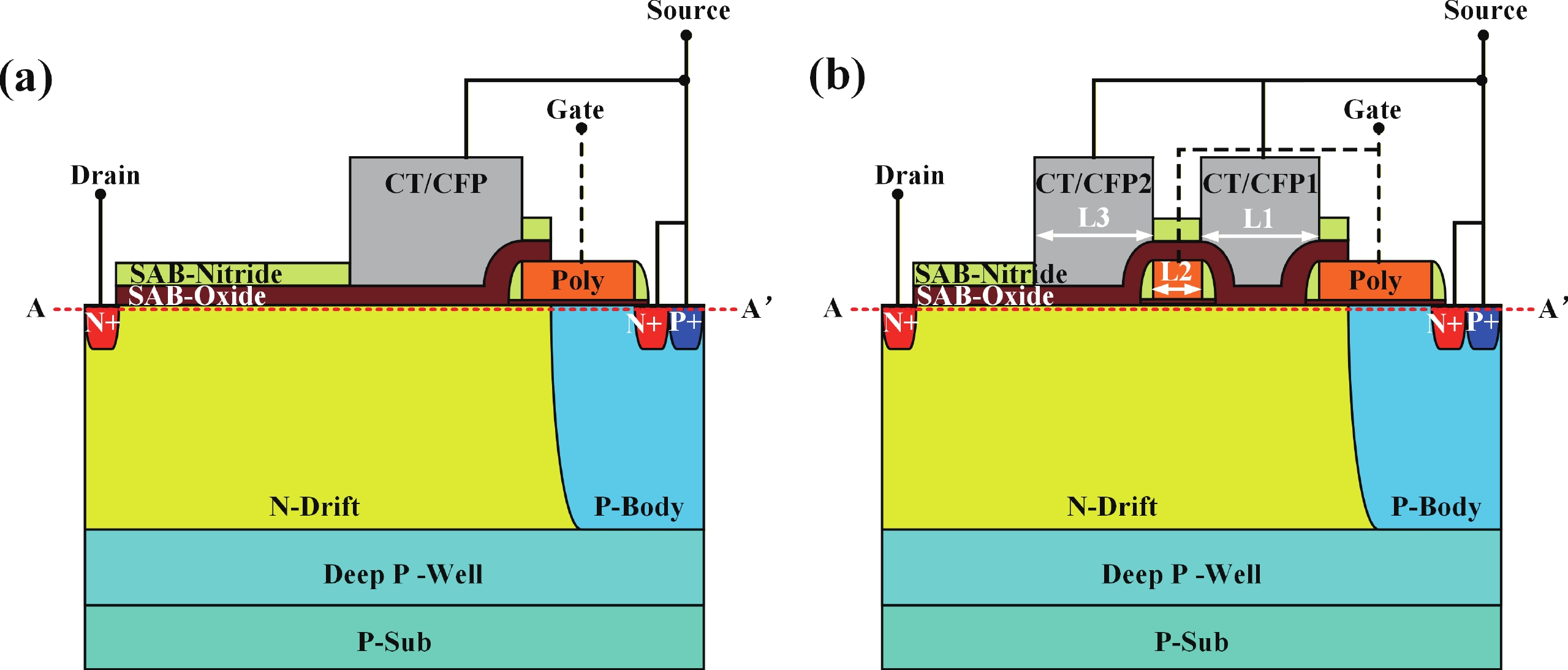
Fig. 1.
(Color online) Cross-sectional schematics of (a) the conventional and (b) proposed CFP-LDMOS.
ARTICLES
Yiting Ye1, Xiaoyun Huang1, Yixian Song1 and Kai Xu1, 2, 3,
Corresponding author: Kai Xu, xuk@zju.edu.cn
Abstract: To improve the breakdown voltage (BV)−specific on-resistance (Ron,sp) trade-off and enhance manufacturability, this article proposes a novel lateral diffused metal−oxide−semiconductor (LDMOS) structure that features a split gate and split contact field plate (CFP). This novel structure requires no additional bias voltages, masks, or process steps, making it fully compatible with the bipolar-CMOS-DMOS (BCD) process flow. The physical mechanisms are elucidated through technology computer-aided design (TCAD) simulations. In the on-state, the positively biased split gate forms an accumulation layer at the drift region surface, thereby reducing Ron,sp. In the off-state, both the split gate and split CFP introduce additional electric-field peaks that smooth the lateral electric field, thus preserving a high BV. Compared with the conventional CFP-LDMOS, the proposed CFP-LDMOS achieves an 8.52% reduction in Ron,sp without compromising BV, leading to an 8.07% improvement in the figure of merit (FOM). Notably, the proposed structure can be extended to LDMOS devices across different voltage levels within BCD platforms, demonstrating its broad applicability.
Keywords: lateral diffused metal−oxide−semiconductor (LDMOS), specific on-resistance (Ron,sp), breakdown voltage (BV), split gate, contact field plate (CFP)
| [1] |
Duan B X, Cao Z, Yuan X, et al. New superjunction LDMOS breaking silicon limit by electric field modulation of buffered step doping. IEEE Electron Device Lett, 2015, 36(1): 47 doi: 10.1109/LED.2014.2366298
|
| [2] |
Kaushal K N, Mohapatra N R. Unified theory of the capacitance behavior in LDMOS devices. IEEE Trans Electron Devices, 2022, 69(1): 39 doi: 10.1109/TED.2021.3131302
|
| [3] |
Chen S Y, Liao B, Dong J C, et al. Study on 20 V LDMOS with stepped-gate-oxide structure for PMIC applications: Design, fabrication, and characterization. IEEE Trans Electron Devices, 2022, 69(2): 878 doi: 10.1109/TED.2021.3131922
|
| [4] |
Ma J, Zhang L, Gu Y, et al. 200 V all-SiC floating gate driver process platform on 4H-SiC P-epi/N+ substate for high-temperature applications. IEEE Trans Electron Devices, 2024, 71(8): 5138 doi: 10.1109/TED.2024.3418297
|
| [5] |
Williams R K, Darwish M N, Blanchard R A, et al. The trench power MOSFET: Part II: Application specific VDMOS, LDMOS, packaging, and reliability. IEEE Trans Electron Devices, 2017, 64(3): 692 doi: 10.1109/TED.2017.2655149
|
| [6] |
Chuang P J, Saadat A, Ghazvini S, et al. Determining the performance limits of LDMOS with three common types of field oxides. IEEE Trans Electron Devices, 2024, 71(4): 2315 doi: 10.1109/TED.2024.3370133
|
| [7] |
Disney D, Letavic T, Trajkovic T, et al. High-voltage integrated circuits: History, state of the art, and future prospects. IEEE Trans Electron Devices, 2017, 64(3): 659 doi: 10.1109/TED.2016.2631125
|
| [8] |
Kaushal K N, Mohapatra N R. A zero-cost technique to improve ON-state performance and reliability of power LDMOS transistors. IEEE J Electron Devices Soc, 2021, 9: 334 doi: 10.1109/JEDS.2021.3059854
|
| [9] |
Wei J, Dai K W, Luo X R, et al. Analyses and experiments of ultralow specific on-resistance LDMOS with integrated diodes. IEEE J Electron Devices Soc, 2021, 9: 1161 doi: 10.1109/JEDS.2021.3114738
|
| [10] |
Liu S Y, Ye R, Sun W F, et al. A novel lateral DMOS transistor with H-shape shallow-trench-isolation structure. IEEE Trans Electron Devices, 2018, 65(11): 5218 doi: 10.1109/TED.2018.2871501
|
| [11] |
Jin F, Liu D H, Xing J J, et al. Best-in-class LDMOS with ultra-shallow trench isolation and p-buried layer from 18V to 40V in 0.18μm BCD technology. 2017 29th International Symposium on Power Semiconductor Devices and IC’s (ISPSD), 2017: 295 doi: 10.23919/ISPSD.2017.7988962
|
| [12] |
Wei L, Chao C, Singh U, et al. A novel contact field plate application in drain-extended-MOSFET transistors. 2017 29th International Symposium on Power Semiconductor Devices and IC’s (ISPSD), 2017: 335 doi: 10.23919/ISPSD.2017.7988957
|
| [13] |
Hébert F, Parvarandeh P, Li M, et al. Building blocks of past, present and future BCD technologies. 2021 33rd International Symposium on Power Semiconductor Devices and ICs (ISPSD), 2021: 11 doi: 10.23919/ISPSD50666.2021.9452276
|
| [14] |
Yu S X, Shao W H, Chen R S, et al. Design and simulation optimization of an ultra-low specific on-resistance LDMOS device. IEEE J Electron Devices Soc, 2024, 12: 14 doi: 10.1109/JEDS.2023.3337341
|
| [15] |
Patel R, Mohapatra N R. Novel step field plate RF LDMOS transistor for improved BVDS-Ron tradeoff and RF performance. IEEE Trans Electron Devices, 2022, 69(8): 4401 doi: 10.1109/TED.2022.3182296
|
| [16] |
Hara K, Kakegawa T, Wada S, et al. Low on-resistance high voltage thin layer SOI LDMOS transistors with stepped field plates. 2017 29th International Symposium on Power Semiconductor Devices and IC’s (ISPSD), 2017: 307 doi: 10.23919/ISPSD.2017.7988965
|
| [17] |
Mori T, Fujii H, Kubo S, et al. Investigation into HCl improvement by a split-reeessed-gate structure in an STI-based nLDMOSFET. 2017 29th International Symposium on Power Semiconductor Devices and IC’s (ISPSD), 2017: 459 doi: 10.23919/ISPSD.2017.7988878
|
| [18] |
Ferrara A, Heringa A, Boksteen B K, et al. The boost transistor: A field plate controlled LDMOST. 2015 27th International Symposium on Power Semiconductor Devices & IC’s (ISPSD), 2015: 165 doi: 10.1109/ISPSD.2015.7123415
|
| [19] |
Wei T. LDMOS of 34mΩ-cm2 on-resistance with 700V breakdown voltage. 2024 36th International Symposium on Power Semiconductor Devices and ICs (ISPSD), 2024: 398 doi: 10.1109/ISPSD59661.2024.10579641
|
| [20] |
Hölke A. Field plate engineering for free metal routing over lateral HV devices. 2024 36th International Symposium on Power Semiconductor Devices and ICs (ISPSD), 2024: 450 doi: 10.1109/ISPSD59661.2024.10579611
|
| [21] |
Zhang C W, Guo H J, Chen Z X, et al. Super field plate technique that can provide charge balance effect for lateral power devices without occupying drift region. IEEE Trans Electron Devices, 2020, 67(5): 2218 doi: 10.1109/TED.2020.2981264
|
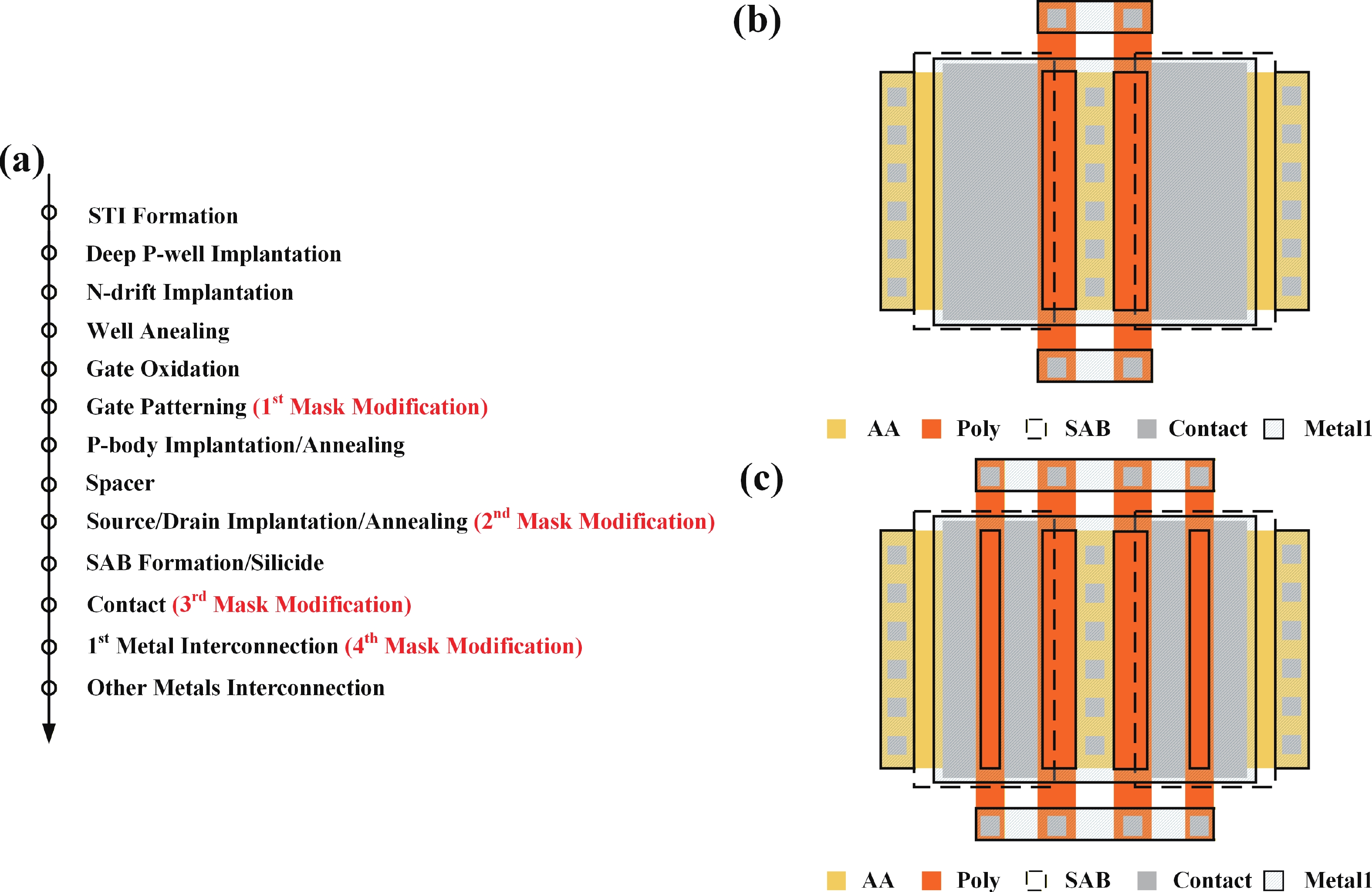
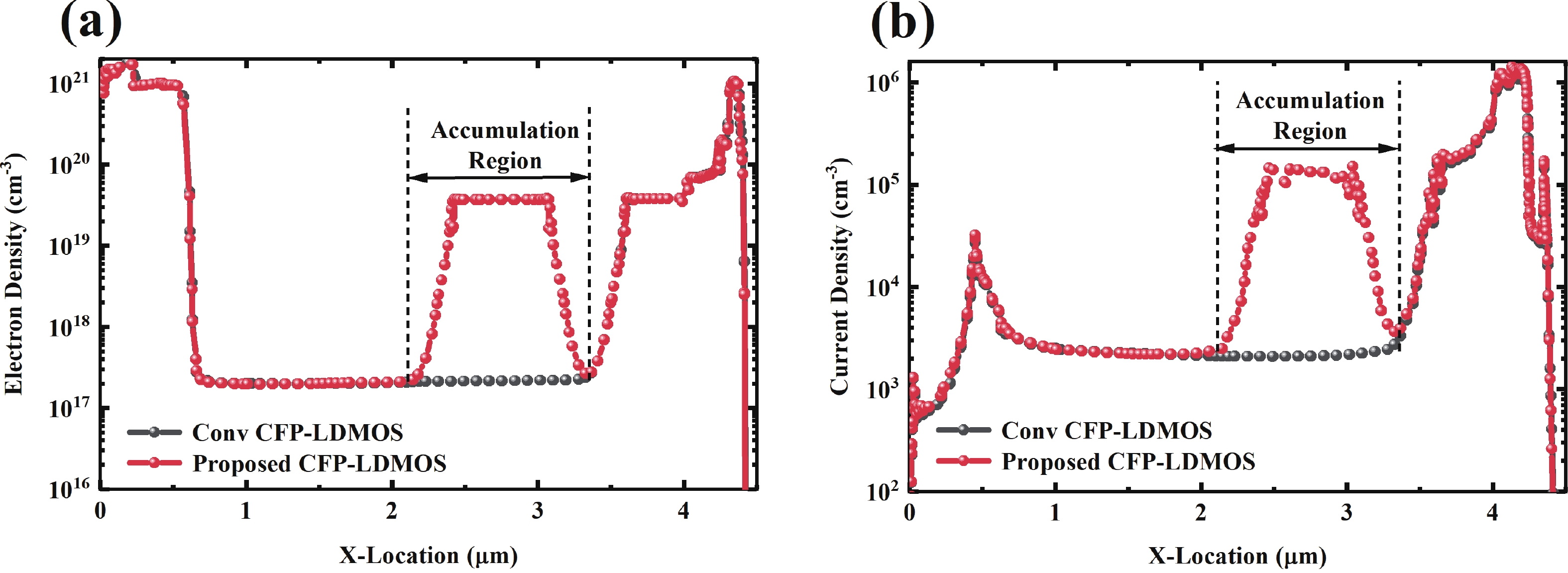
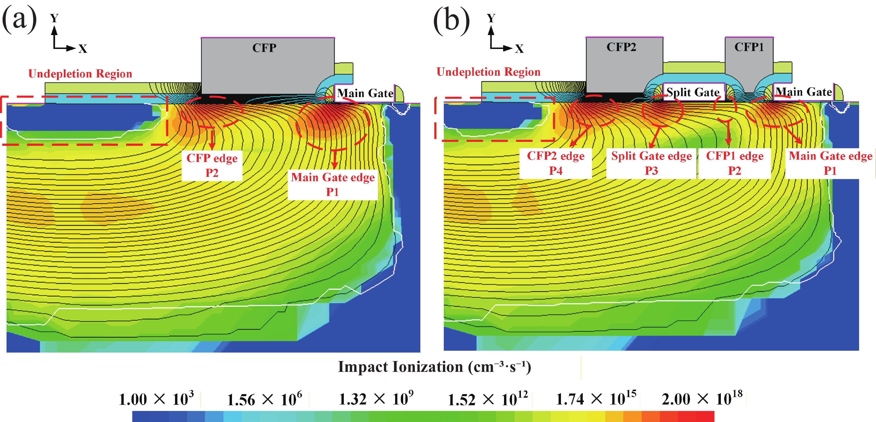
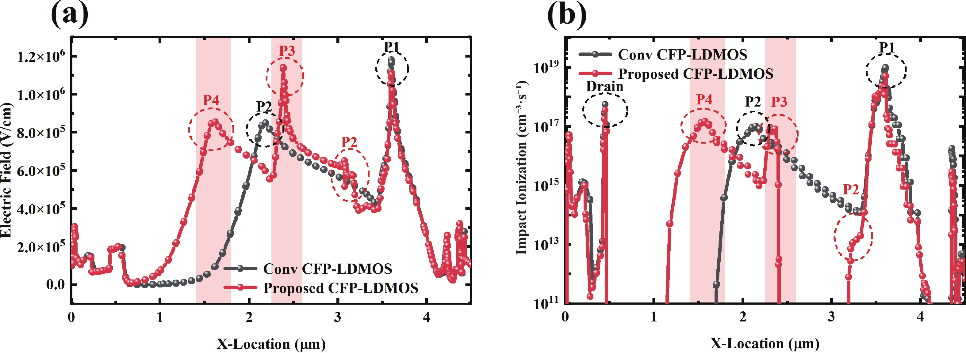
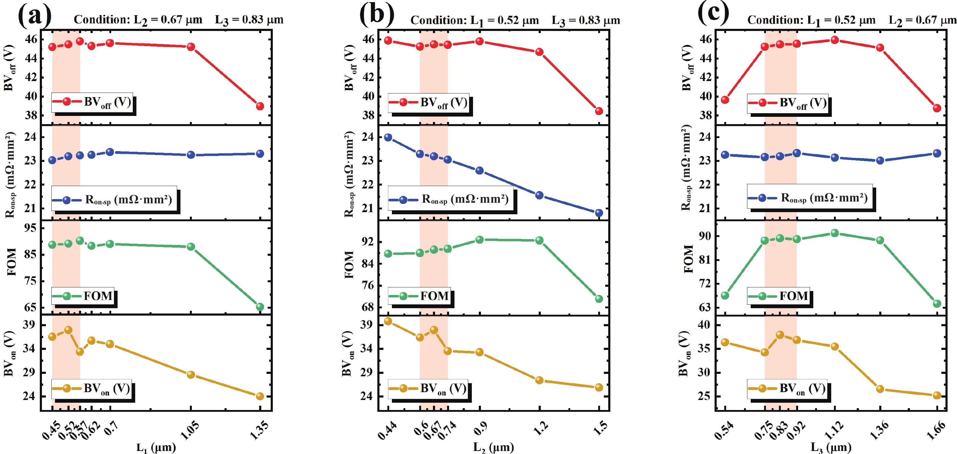
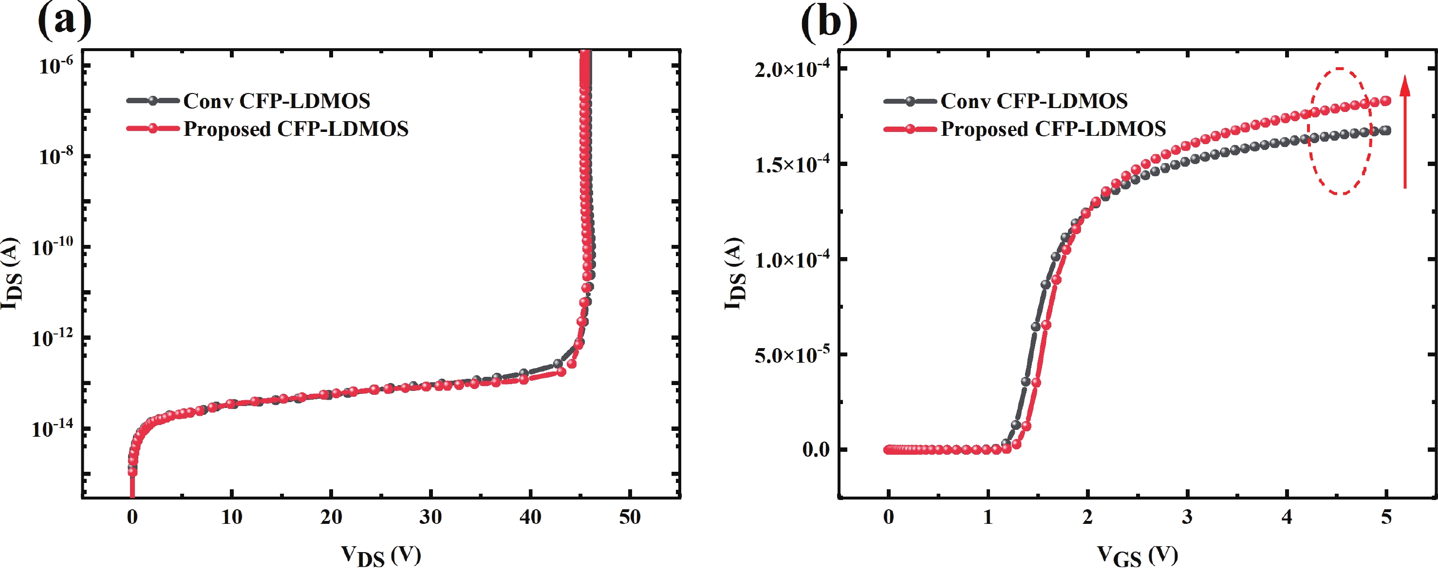
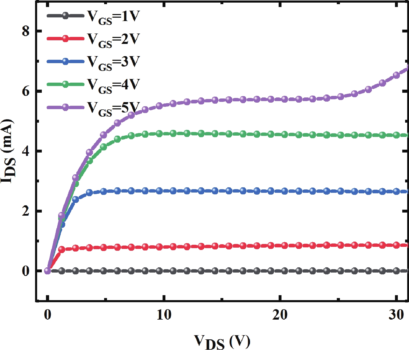
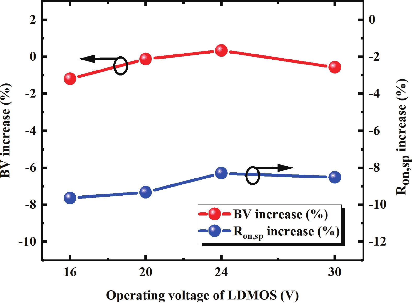
Table 1. Main parameters used for the proposed CFP-LDMOS.
| Label | Parameter | Value (µm) |
| L1 | The length of the first CFP | 0.52 |
| L2 | The length of the split gate | 0.67 |
| L3 | The length of the second CFP | 0.83 |
 DownLoad: CSV
| [1] |
Duan B X, Cao Z, Yuan X, et al. New superjunction LDMOS breaking silicon limit by electric field modulation of buffered step doping. IEEE Electron Device Lett, 2015, 36(1): 47 doi: 10.1109/LED.2014.2366298
|
| [2] |
Kaushal K N, Mohapatra N R. Unified theory of the capacitance behavior in LDMOS devices. IEEE Trans Electron Devices, 2022, 69(1): 39 doi: 10.1109/TED.2021.3131302
|
| [3] |
Chen S Y, Liao B, Dong J C, et al. Study on 20 V LDMOS with stepped-gate-oxide structure for PMIC applications: Design, fabrication, and characterization. IEEE Trans Electron Devices, 2022, 69(2): 878 doi: 10.1109/TED.2021.3131922
|
| [4] |
Ma J, Zhang L, Gu Y, et al. 200 V all-SiC floating gate driver process platform on 4H-SiC P-epi/N+ substate for high-temperature applications. IEEE Trans Electron Devices, 2024, 71(8): 5138 doi: 10.1109/TED.2024.3418297
|
| [5] |
Williams R K, Darwish M N, Blanchard R A, et al. The trench power MOSFET: Part II: Application specific VDMOS, LDMOS, packaging, and reliability. IEEE Trans Electron Devices, 2017, 64(3): 692 doi: 10.1109/TED.2017.2655149
|
| [6] |
Chuang P J, Saadat A, Ghazvini S, et al. Determining the performance limits of LDMOS with three common types of field oxides. IEEE Trans Electron Devices, 2024, 71(4): 2315 doi: 10.1109/TED.2024.3370133
|
| [7] |
Disney D, Letavic T, Trajkovic T, et al. High-voltage integrated circuits: History, state of the art, and future prospects. IEEE Trans Electron Devices, 2017, 64(3): 659 doi: 10.1109/TED.2016.2631125
|
| [8] |
Kaushal K N, Mohapatra N R. A zero-cost technique to improve ON-state performance and reliability of power LDMOS transistors. IEEE J Electron Devices Soc, 2021, 9: 334 doi: 10.1109/JEDS.2021.3059854
|
| [9] |
Wei J, Dai K W, Luo X R, et al. Analyses and experiments of ultralow specific on-resistance LDMOS with integrated diodes. IEEE J Electron Devices Soc, 2021, 9: 1161 doi: 10.1109/JEDS.2021.3114738
|
| [10] |
Liu S Y, Ye R, Sun W F, et al. A novel lateral DMOS transistor with H-shape shallow-trench-isolation structure. IEEE Trans Electron Devices, 2018, 65(11): 5218 doi: 10.1109/TED.2018.2871501
|
| [11] |
Jin F, Liu D H, Xing J J, et al. Best-in-class LDMOS with ultra-shallow trench isolation and p-buried layer from 18V to 40V in 0.18μm BCD technology. 2017 29th International Symposium on Power Semiconductor Devices and IC’s (ISPSD), 2017: 295 doi: 10.23919/ISPSD.2017.7988962
|
| [12] |
Wei L, Chao C, Singh U, et al. A novel contact field plate application in drain-extended-MOSFET transistors. 2017 29th International Symposium on Power Semiconductor Devices and IC’s (ISPSD), 2017: 335 doi: 10.23919/ISPSD.2017.7988957
|
| [13] |
Hébert F, Parvarandeh P, Li M, et al. Building blocks of past, present and future BCD technologies. 2021 33rd International Symposium on Power Semiconductor Devices and ICs (ISPSD), 2021: 11 doi: 10.23919/ISPSD50666.2021.9452276
|
| [14] |
Yu S X, Shao W H, Chen R S, et al. Design and simulation optimization of an ultra-low specific on-resistance LDMOS device. IEEE J Electron Devices Soc, 2024, 12: 14 doi: 10.1109/JEDS.2023.3337341
|
| [15] |
Patel R, Mohapatra N R. Novel step field plate RF LDMOS transistor for improved BVDS-Ron tradeoff and RF performance. IEEE Trans Electron Devices, 2022, 69(8): 4401 doi: 10.1109/TED.2022.3182296
|
| [16] |
Hara K, Kakegawa T, Wada S, et al. Low on-resistance high voltage thin layer SOI LDMOS transistors with stepped field plates. 2017 29th International Symposium on Power Semiconductor Devices and IC’s (ISPSD), 2017: 307 doi: 10.23919/ISPSD.2017.7988965
|
| [17] |
Mori T, Fujii H, Kubo S, et al. Investigation into HCl improvement by a split-reeessed-gate structure in an STI-based nLDMOSFET. 2017 29th International Symposium on Power Semiconductor Devices and IC’s (ISPSD), 2017: 459 doi: 10.23919/ISPSD.2017.7988878
|
| [18] |
Ferrara A, Heringa A, Boksteen B K, et al. The boost transistor: A field plate controlled LDMOST. 2015 27th International Symposium on Power Semiconductor Devices & IC’s (ISPSD), 2015: 165 doi: 10.1109/ISPSD.2015.7123415
|
| [19] |
Wei T. LDMOS of 34mΩ-cm2 on-resistance with 700V breakdown voltage. 2024 36th International Symposium on Power Semiconductor Devices and ICs (ISPSD), 2024: 398 doi: 10.1109/ISPSD59661.2024.10579641
|
| [20] |
Hölke A. Field plate engineering for free metal routing over lateral HV devices. 2024 36th International Symposium on Power Semiconductor Devices and ICs (ISPSD), 2024: 450 doi: 10.1109/ISPSD59661.2024.10579611
|
| [21] |
Zhang C W, Guo H J, Chen Z X, et al. Super field plate technique that can provide charge balance effect for lateral power devices without occupying drift region. IEEE Trans Electron Devices, 2020, 67(5): 2218 doi: 10.1109/TED.2020.2981264
|


Article views: 1065 Times PDF downloads: 274 Times Cited by: 0 Times
Received: 26 August 2025 Revised: 01 December 2025 Online: Accepted Manuscript: 31 January 2026Uncorrected proof: 26 February 2026Published: 14 May 2026
| Citation: |
Yiting Ye, Xiaoyun Huang, Yixian Song, Kai Xu. A novel split gate and contact-field-plate LDMOS with enhanced BV−Ron,sp trade-off and improved FOM[J]. Journal of Semiconductors, 2026, 47(5): 052301. doi: 10.1088/1674-4926/25080033
****
Y T Ye, X Y Huang, Y X Song, and K Xu, A novel split gate and contact-field-plate LDMOS with enhanced BV−Ron,sp trade-off and improved FOM[J]. J. Semicond., 2026, 47(5): 052301 doi: 10.1088/1674-4926/25080033

|
 Yiting Ye got her BS degree from Central South University in 2024. Now she is a Master student at Zhejiang University under the supervision of Prof. Kai Xu. Her research focuses on lateral diffused metal−oxide−semiconductor (LDMOS) transistors
 Kai Xu got his PhD degree in 2017 at the National Center for Nanoscience and Technology. Then he went to University of Illinois Urbana-Champaign as a postdoc. In October 2021, he joined ZJU-Hangzhou Global Scientific and Technological Innovation Center as independent principal investigator. His research interests include semiconductor power devices and integration, intelligent manufacturing of integrated circuits and heterogeneous integration
| [1] |
Duan B X, Cao Z, Yuan X, et al. New superjunction LDMOS breaking silicon limit by electric field modulation of buffered step doping. IEEE Electron Device Lett, 2015, 36(1): 47 doi: 10.1109/LED.2014.2366298
|
| [2] |
Kaushal K N, Mohapatra N R. Unified theory of the capacitance behavior in LDMOS devices. IEEE Trans Electron Devices, 2022, 69(1): 39 doi: 10.1109/TED.2021.3131302
|
| [3] |
Chen S Y, Liao B, Dong J C, et al. Study on 20 V LDMOS with stepped-gate-oxide structure for PMIC applications: Design, fabrication, and characterization. IEEE Trans Electron Devices, 2022, 69(2): 878 doi: 10.1109/TED.2021.3131922
|
| [4] |
Ma J, Zhang L, Gu Y, et al. 200 V all-SiC floating gate driver process platform on 4H-SiC P-epi/N+ substate for high-temperature applications. IEEE Trans Electron Devices, 2024, 71(8): 5138 doi: 10.1109/TED.2024.3418297
|
| [5] |
Williams R K, Darwish M N, Blanchard R A, et al. The trench power MOSFET: Part II: Application specific VDMOS, LDMOS, packaging, and reliability. IEEE Trans Electron Devices, 2017, 64(3): 692 doi: 10.1109/TED.2017.2655149
|
| [6] |
Chuang P J, Saadat A, Ghazvini S, et al. Determining the performance limits of LDMOS with three common types of field oxides. IEEE Trans Electron Devices, 2024, 71(4): 2315 doi: 10.1109/TED.2024.3370133
|
| [7] |
Disney D, Letavic T, Trajkovic T, et al. High-voltage integrated circuits: History, state of the art, and future prospects. IEEE Trans Electron Devices, 2017, 64(3): 659 doi: 10.1109/TED.2016.2631125
|
| [8] |
Kaushal K N, Mohapatra N R. A zero-cost technique to improve ON-state performance and reliability of power LDMOS transistors. IEEE J Electron Devices Soc, 2021, 9: 334 doi: 10.1109/JEDS.2021.3059854
|
| [9] |
Wei J, Dai K W, Luo X R, et al. Analyses and experiments of ultralow specific on-resistance LDMOS with integrated diodes. IEEE J Electron Devices Soc, 2021, 9: 1161 doi: 10.1109/JEDS.2021.3114738
|
| [10] |
Liu S Y, Ye R, Sun W F, et al. A novel lateral DMOS transistor with H-shape shallow-trench-isolation structure. IEEE Trans Electron Devices, 2018, 65(11): 5218 doi: 10.1109/TED.2018.2871501
|
| [11] |
Jin F, Liu D H, Xing J J, et al. Best-in-class LDMOS with ultra-shallow trench isolation and p-buried layer from 18V to 40V in 0.18μm BCD technology. 2017 29th International Symposium on Power Semiconductor Devices and IC’s (ISPSD), 2017: 295 doi: 10.23919/ISPSD.2017.7988962
|
| [12] |
Wei L, Chao C, Singh U, et al. A novel contact field plate application in drain-extended-MOSFET transistors. 2017 29th International Symposium on Power Semiconductor Devices and IC’s (ISPSD), 2017: 335 doi: 10.23919/ISPSD.2017.7988957
|
| [13] |
Hébert F, Parvarandeh P, Li M, et al. Building blocks of past, present and future BCD technologies. 2021 33rd International Symposium on Power Semiconductor Devices and ICs (ISPSD), 2021: 11 doi: 10.23919/ISPSD50666.2021.9452276
|
| [14] |
Yu S X, Shao W H, Chen R S, et al. Design and simulation optimization of an ultra-low specific on-resistance LDMOS device. IEEE J Electron Devices Soc, 2024, 12: 14 doi: 10.1109/JEDS.2023.3337341
|
| [15] |
Patel R, Mohapatra N R. Novel step field plate RF LDMOS transistor for improved BVDS-Ron tradeoff and RF performance. IEEE Trans Electron Devices, 2022, 69(8): 4401 doi: 10.1109/TED.2022.3182296
|
| [16] |
Hara K, Kakegawa T, Wada S, et al. Low on-resistance high voltage thin layer SOI LDMOS transistors with stepped field plates. 2017 29th International Symposium on Power Semiconductor Devices and IC’s (ISPSD), 2017: 307 doi: 10.23919/ISPSD.2017.7988965
|
| [17] |
Mori T, Fujii H, Kubo S, et al. Investigation into HCl improvement by a split-reeessed-gate structure in an STI-based nLDMOSFET. 2017 29th International Symposium on Power Semiconductor Devices and IC’s (ISPSD), 2017: 459 doi: 10.23919/ISPSD.2017.7988878
|
| [18] |
Ferrara A, Heringa A, Boksteen B K, et al. The boost transistor: A field plate controlled LDMOST. 2015 27th International Symposium on Power Semiconductor Devices & IC’s (ISPSD), 2015: 165 doi: 10.1109/ISPSD.2015.7123415
|
| [19] |
Wei T. LDMOS of 34mΩ-cm2 on-resistance with 700V breakdown voltage. 2024 36th International Symposium on Power Semiconductor Devices and ICs (ISPSD), 2024: 398 doi: 10.1109/ISPSD59661.2024.10579641
|
| [20] |
Hölke A. Field plate engineering for free metal routing over lateral HV devices. 2024 36th International Symposium on Power Semiconductor Devices and ICs (ISPSD), 2024: 450 doi: 10.1109/ISPSD59661.2024.10579611
|
| [21] |
Zhang C W, Guo H J, Chen Z X, et al. Super field plate technique that can provide charge balance effect for lateral power devices without occupying drift region. IEEE Trans Electron Devices, 2020, 67(5): 2218 doi: 10.1109/TED.2020.2981264
|

 WeChat ID
Journal of Semiconductors © 2017 All Rights Reserved 京ICP备05085259号-2


