


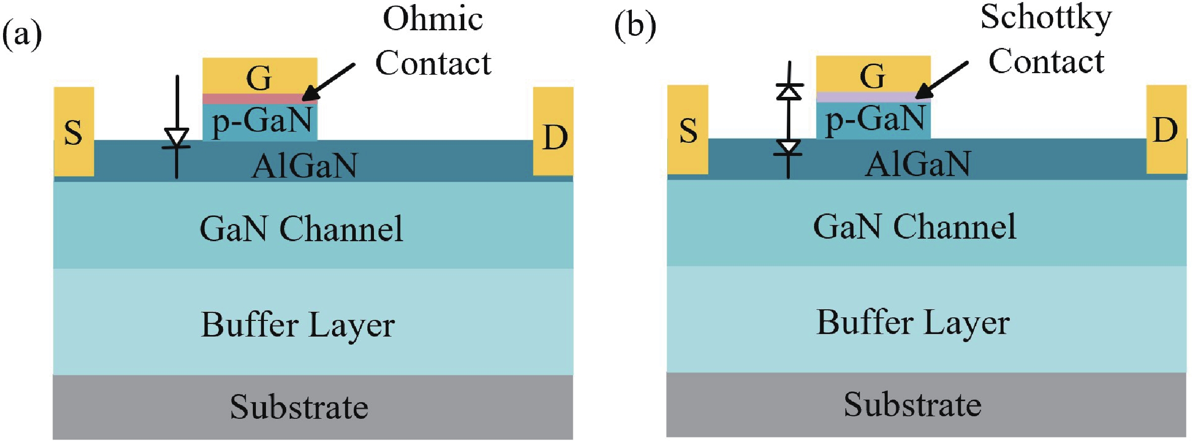
Fig. 1.
(Color online) The p-GaN gate stack structures of (a) ohmic contact and (b) Schottky contact.
ARTICLES
Xuejing Sun1, Shenglei Zhao1, 2, , Yinhe Wu2, , Longyang Yu1, 2, Juan Gui1, Ga Zhang1, Xiufeng Song1, Shuzhen You2, Song Yang3, Hui Sun3, Bin Hu3, Huantao Duan3, Jin Rao3, Zhen Chen3, Yue Hao1 and Jincheng Zhang1, 2
Corresponding author: Shenglei Zhao, slzhao@xidian.edu.cn; Yinhe Wu, wuyinhe@xidian.edu.cn
Abstract: In this paper, a novel gate-series-diode structure for the Schottky-type p-GaN HEMTs is proposed, and the impact of the proposed structure on gate−source voltage oscillation is investigated when the device is turned on. The proposed structure is capable of effectively mitigating the gate−source voltage overshoot problem of GaN device, and has little effect on the switching characteristics. The gate voltage oscillations can be greatly stabilized at the steady-state turn-on voltage level when the turn-on voltage is 5 V. Compared with the conventional structure, the overshoots of the proposed structure reduce by 31.4%−71.4% and 40.6%−80.4% respectively under the two pulses, as drain−source voltage rises. The proposed structure is proved to be a potential method on improving gate reliability of the most GaN power devices.
Keywords: p-GaN high-electron-mobility transistors (p-GaN HEMTs), schottky-type contact, gate-series-diode, gate reliability
| [1] |
Chen K J, Häberlen O, Lidow A, et al. GaN-on-Si power technology: Devices and applications. IEEE Trans Electron Devices, 2017, 64(3): 779 doi: 10.1109/TED.2017.2657579
|
| [2] |
Jones E A, Wang F, Ozpineci B. Application-based review of GaN HFETs. 2014 IEEE Workshop on Wide Bandgap Power Devices and Applications, 2014: 24 doi: 10.1109/WiPDA.2014.6964617
|
| [3] |
Yan Z H, Yuan S, Jiang X, et al. A novel AlGaN/GaN-based Schottky barrier diode with partial P-GaN cap layer and semicircular T-anode for temperature sensors. IEEE Trans Electron Devices, 2023, 70(10): 5087 doi: 10.1109/TED.2023.3306736
|
| [4] |
Meneghesso G, Verzellesi G, Danesin F, et al. Reliability of GaN high-electron-mobility transistors: State of the art and perspectives. IEEE Trans Device Mater Reliab, 2008, 8(2): 332 doi: 10.1109/TDMR.2008.923743
|
| [5] |
Li B Y, Yang X, Wang K P, et al. A compact double-sided cooling 650V/30A GaN power module with low parasitic parameters. IEEE Trans Power Electron, 2022, 37(1): 426 doi: 10.1109/TPEL.2021.3092367
|
| [6] |
Liu X, Xu S R, Zhang T, et al. Demonstration of a GaN-based P-channel FinFET with high current density based on multi-channel structure. Appl Phys Lett, 2025, 126(20): 202103 doi: 10.1063/5.0258789
|
| [7] |
Wu N T, Luo L, Xing Z H, et al. Enhanced performance of low-leakage-current normally off p-GaN gate HEMTs using NH3 plasma pretreatment. IEEE Trans Electron Devices, 2023, 70(9): 4560 doi: 10.1109/TED.2023.3294894
|
| [8] |
Cheng Y, He J B, Xu H, et al. Gate reliability of Schottky-type p-GaN gate HEMTs under AC positive gate bias stress with a switching drain bias. IEEE Electron Device Lett, 2022, 43(9): 1404 doi: 10.1109/LED.2022.3188555
|
| [9] |
Zhou F, Xu W Z, Jin Y L, et al. 3.0-V-threshold-voltage p-GaN HEMTs with low-loss reverse conduction capability. 2023 35th International Symposium on Power Semiconductor Devices and ICs (ISPSD), 2023: 370 doi: 10.1109/ISPSD57135.2023.10147450
|
| [10] |
Wang H D, Gao H W, Chen X, et al. Enhanced gate reliability of ohmic-like p-GaN gate HEMT with a built-in reverse diode. IEEE Trans Electron Devices, 2024, 71(4): 2355 doi: 10.1109/TED.2024.3365454
|
| [11] |
Zhang L, Zheng Z Y, Yang S, et al. P-GaN gate HEMT with surface reinforcement for enhanced gate reliability. IEEE Electron Device Lett, 2021, 42(1): 22 doi: 10.1109/LED.2020.3037186
|
| [12] |
Chao X, Tang C K, Tan J J, et al. Analysis of VTH degradation and recovery behaviors of p-GaN gate HEMTs under forward gate bias. IEEE Trans Electron Devices, 2023, 70(6): 2970 doi: 10.1109/TED.2023.3263819
|
| [13] |
Wang H, Yin Y L, Ji F W, et al. Enhanced gate breakdown and electroluminescence in p-GaN gate HEMTs under pulsed switching conditions. 2023 35th International Symposium on Power Semiconductor Devices and ICs (ISPSD), 2023: 91 doi: 10.1109/ISPSD57135.2023.10147654
|
| [14] |
Qi Z Y, Pei Y Q, Wang L L, et al. A highly integrated PCB embedded GaN full-bridge module with ultralow parasitic inductance. IEEE Trans Power Electron, 2022, 37(4): 4161 doi: 10.1109/TPEL.2021.3128694
|
| [15] |
Wang K P, Wang L L, Yang X, et al. A multiloop method for minimization of parasitic inductance in GaN-based high-frequency DC–DC converter. IEEE Trans Power Electron, 2017, 32(6): 4728 doi: 10.1109/TPEL.2016.2597183
|
| [16] |
Kwan A M H, Chen K J. A gate overdrive protection technique for improved reliability in AlGaN/GaN enhancement-mode HEMTs. IEEE Electron Device Lett, 2013, 34(1): 30 doi: 10.1109/LED.2012.2224632
|
| [17] |
Zhou G N, Zeng F M, Gao R Y, et al. P-GaN gate HEMTs with 10.6 V maximum gate drive voltages by Mg doping engineering. IEEE Trans Electron Devices, 2022, 69(5): 2282 doi: 10.1109/TED.2022.3157569
|
| [18] |
Wang C C, Hua M Y, Chen J T, et al. E-mode p-n junction/AlGaN/GaN (PNJ) HEMTs. IEEE Electron Device Lett, 2020, 41(4): 545 doi: 10.1109/LED.2020.2977143
|
| [19] |
Liu C H, Chiu H C, Wang H C, et al. Improved gate reliability normally-off p-GaN/AlN/AlGaN/GaN HEMT with AlGaN cap-layer. IEEE Electron Device Lett, 2021, 42(10): 1432 doi: 10.1109/LED.2021.3109054
|
| [20] |
Yang Q S, Wang L L, Qi Z Y, et al. Analysis of gate-source voltage spike generated by miller capacitance and common source inductance. 2021 IEEE 12th Energy Conversion Congress & Exposition-Asia (ECCE-Asia), 2021: 1293 doi: 10.1109/ECCE-Asia49820.2021.9479360
|
| [21] |
Zhang W, Huang X C, Lee F C, et al. Gate drive design considerations for high voltage cascode GaN HEMT. 2014 IEEE Applied Power Electronics Conference and Exposition-APEC 2014, 2014: 1484 doi: 10.1109/APEC.2014.6803503
|
| [22] |
Zhou F, Xu W Z, Ren F F, et al. 1.2 kV/25 a normally off P-N junction/AlGaN/GaN HEMTs with nanosecond switching characteristics and robust overvoltage capability. IEEE Trans Power Electron, 2022, 37(1): 26 doi: 10.1109/TPEL.2021.3095937
|
| [23] |
Gareau J, Hou R Y, Emadi A. Review of loss distribution, analysis, and measurement techniques for GaN HEMTs. IEEE Trans Power Electron, 2020, 35(7): 7405 doi: 10.1109/TPEL.2019.2954819
|
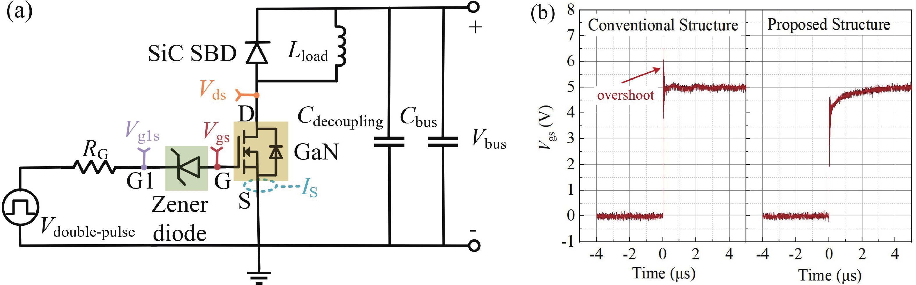
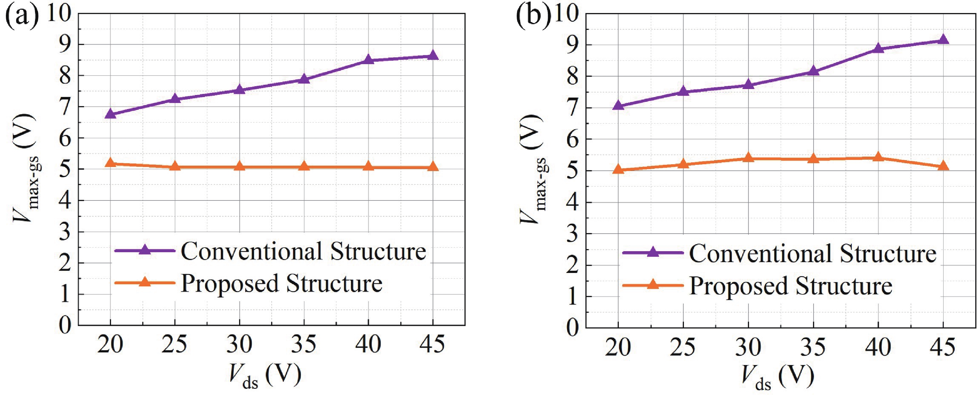
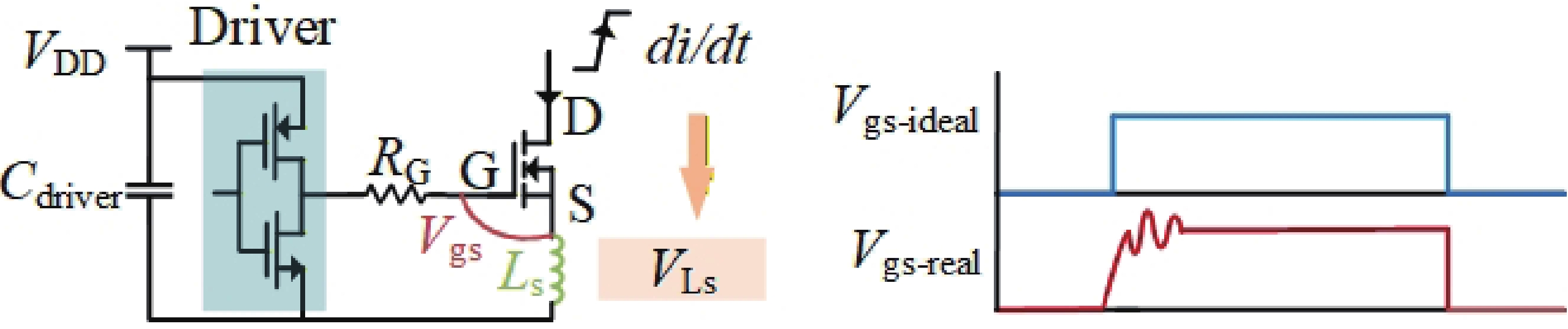
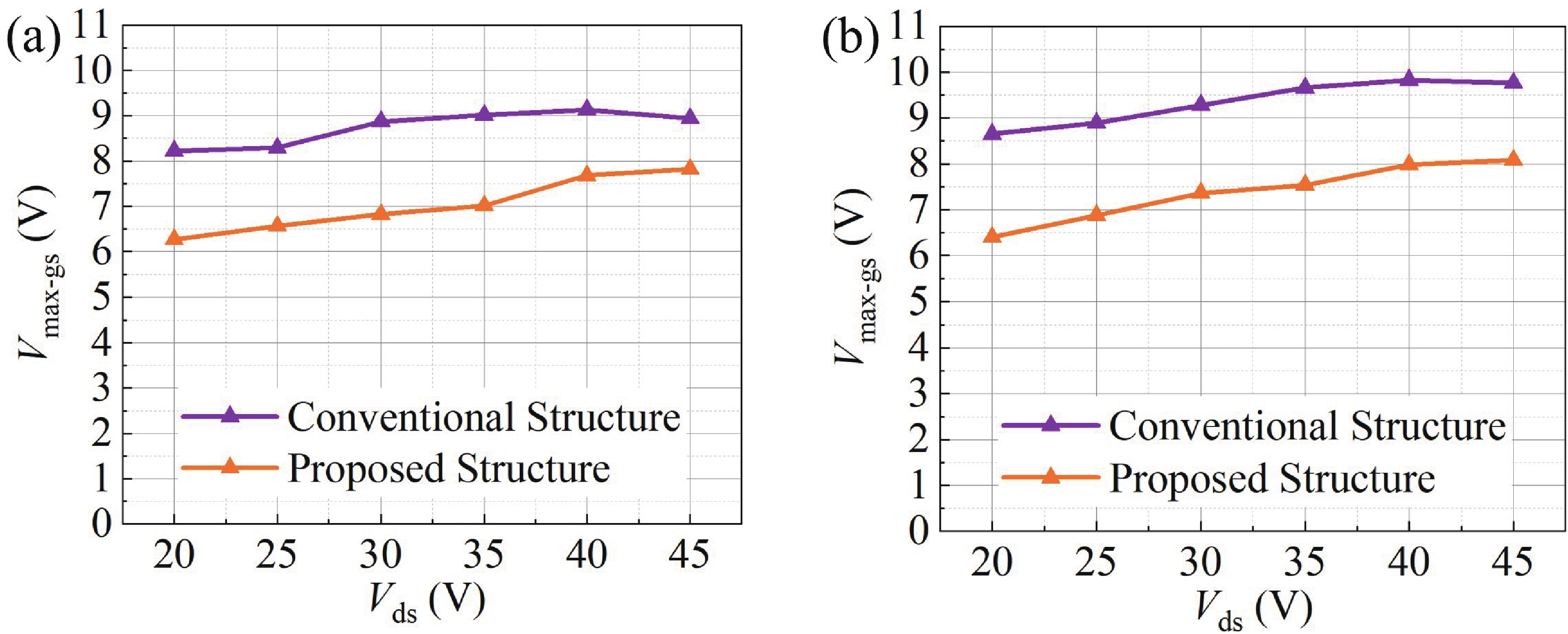
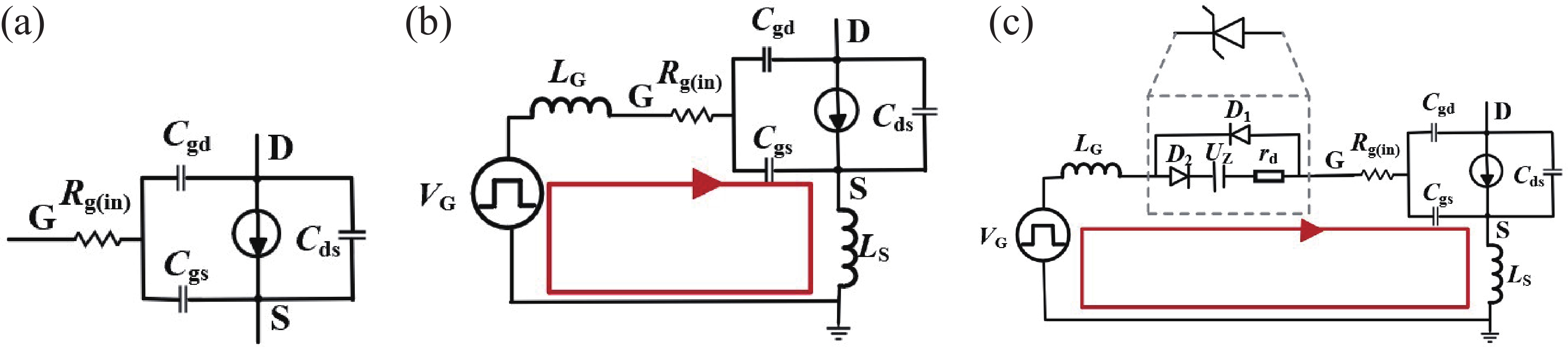
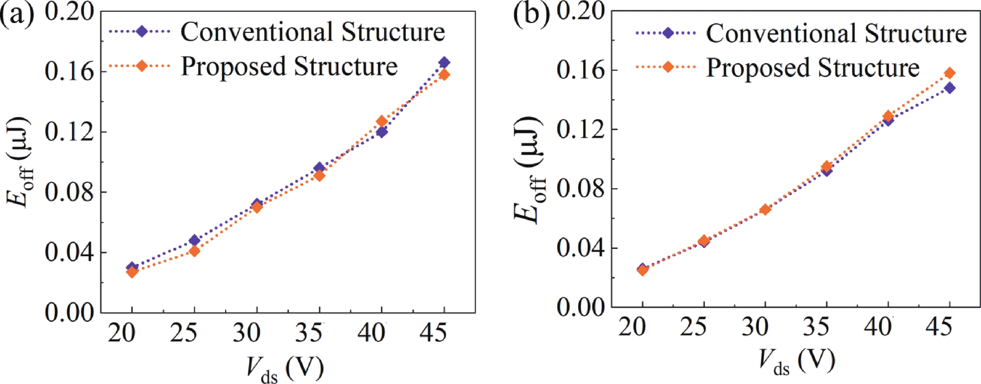
Table 1. The Vmax-gs and overshoot comparisons of conventional and proposed structures when turn-on voltage is 5 V.
| Pulse | Vds(V) | 20 | 25 | 30 | 35 | 40 | 45 | |||
| Under the first pulse |
Conventional structure |
Vmax-gs (V) | 6.74 | 7.23 | 7.52 | 7.86 | 8.48 | 8.62 | ||
| Overshoot | 34.8% | 44.6% | 50.4% | 57.2% | 69.6% | 72.4% | ||||
| Proposed structure |
Vmax-gs (V) | 5.17 | 5.06 | 5.06 | 5.06 | 5.06 | 5.05 | |||
| Overshoot | 3.4% | 1.2% | 1.2% | 1.2% | 1.2% | 1% | ||||
| Reduced overshoot | 43.4% | 49.2% | 56% | 68.4% | 71.4% | 31.4% | ||||
| Under the second pulse |
IS (A) | 1.64 | 2.19 | 2.6 | 3 | 3.3 | 3.78 | |||
| Conventional structure |
Vmax-gs (V) | 7.04 | 7.5 | 7.71 | 8.14 | 8.86 | 9.14 | |||
| Overshoot | 40.8% | 50% | 54.2% | 62.8% | 77.2% | 82.8% | ||||
| Proposed structure |
Vmax-gs (V) | 5.01 | 5.18 | 5.38 | 5.35 | 5.4 | 5.12 | |||
| Overshoot | 0.2% | 3.6% | 7.6% | 7% | 8% | 2.4% | ||||
| Reduced overshoot | 40.6% | 46.4% | 46.6% | 55.8% | 69.2% | 80.4% | ||||
 DownLoad: CSV
Table 2. The Vmax-gs and overshoot comparisons of conventional and proposed structures when turn-on voltage is 6 V.
| Pulse | Vds(V) | 20 | 25 | 30 | 35 | 40 | 45 | |||
| Under the first pulse |
Conventional structure |
Vmax-gs (V) | 8.22 | 8.29 | 8.87 | 9.01 | 9.13 | 9 | ||
| Overshoot | 37% | 38.2% | 47.8% | 50.2% | 52.2% | 50% | ||||
| Proposed structure |
Vmax-gs (V) | 6.27 | 6.56 | 6.82 | 7.01 | 7.68 | 7.82 | |||
| Overshoot | 4.5% | 9.3% | 13.7% | 16.8% | 28% | 30.3% | ||||
| Reduced overshoot | 32.5% | 28.9% | 34.1% | 33.4% | 24.2% | 19.7% | ||||
| Under the second pulse |
IS(A) | 1.64 | 2.19 | 2.6 | 3 | 3.3 | 3.78 | |||
| Conventional structure |
Vmax-gs (V) | 8.65 | 8.89 | 9.28 | 9.66 | 9.83 | 9.76 | |||
| Overshoot | 44.2% | 48.2% | 54.7% | 61% | 63.8% | 62.7% | ||||
| Proposed structure |
Vmax-gs (V) | 6.4 | 6.88 | 7.36 | 7.54 | 7.98 | 8.08 | |||
| Overshoot | 6.7% | 14.7% | 22.7% | 25.7% | 33% | 34.7% | ||||
| Reduced overshoot | 37.5% | 33.5% | 32% | 35.3% | 30.8% | 28% | ||||
DownLoad: CSV
| [1] |
Chen K J, Häberlen O, Lidow A, et al. GaN-on-Si power technology: Devices and applications. IEEE Trans Electron Devices, 2017, 64(3): 779 doi: 10.1109/TED.2017.2657579
|
| [2] |
Jones E A, Wang F, Ozpineci B. Application-based review of GaN HFETs. 2014 IEEE Workshop on Wide Bandgap Power Devices and Applications, 2014: 24 doi: 10.1109/WiPDA.2014.6964617
|
| [3] |
Yan Z H, Yuan S, Jiang X, et al. A novel AlGaN/GaN-based Schottky barrier diode with partial P-GaN cap layer and semicircular T-anode for temperature sensors. IEEE Trans Electron Devices, 2023, 70(10): 5087 doi: 10.1109/TED.2023.3306736
|
| [4] |
Meneghesso G, Verzellesi G, Danesin F, et al. Reliability of GaN high-electron-mobility transistors: State of the art and perspectives. IEEE Trans Device Mater Reliab, 2008, 8(2): 332 doi: 10.1109/TDMR.2008.923743
|
| [5] |
Li B Y, Yang X, Wang K P, et al. A compact double-sided cooling 650V/30A GaN power module with low parasitic parameters. IEEE Trans Power Electron, 2022, 37(1): 426 doi: 10.1109/TPEL.2021.3092367
|
| [6] |
Liu X, Xu S R, Zhang T, et al. Demonstration of a GaN-based P-channel FinFET with high current density based on multi-channel structure. Appl Phys Lett, 2025, 126(20): 202103 doi: 10.1063/5.0258789
|
| [7] |
Wu N T, Luo L, Xing Z H, et al. Enhanced performance of low-leakage-current normally off p-GaN gate HEMTs using NH3 plasma pretreatment. IEEE Trans Electron Devices, 2023, 70(9): 4560 doi: 10.1109/TED.2023.3294894
|
| [8] |
Cheng Y, He J B, Xu H, et al. Gate reliability of Schottky-type p-GaN gate HEMTs under AC positive gate bias stress with a switching drain bias. IEEE Electron Device Lett, 2022, 43(9): 1404 doi: 10.1109/LED.2022.3188555
|
| [9] |
Zhou F, Xu W Z, Jin Y L, et al. 3.0-V-threshold-voltage p-GaN HEMTs with low-loss reverse conduction capability. 2023 35th International Symposium on Power Semiconductor Devices and ICs (ISPSD), 2023: 370 doi: 10.1109/ISPSD57135.2023.10147450
|
| [10] |
Wang H D, Gao H W, Chen X, et al. Enhanced gate reliability of ohmic-like p-GaN gate HEMT with a built-in reverse diode. IEEE Trans Electron Devices, 2024, 71(4): 2355 doi: 10.1109/TED.2024.3365454
|
| [11] |
Zhang L, Zheng Z Y, Yang S, et al. P-GaN gate HEMT with surface reinforcement for enhanced gate reliability. IEEE Electron Device Lett, 2021, 42(1): 22 doi: 10.1109/LED.2020.3037186
|
| [12] |
Chao X, Tang C K, Tan J J, et al. Analysis of VTH degradation and recovery behaviors of p-GaN gate HEMTs under forward gate bias. IEEE Trans Electron Devices, 2023, 70(6): 2970 doi: 10.1109/TED.2023.3263819
|
| [13] |
Wang H, Yin Y L, Ji F W, et al. Enhanced gate breakdown and electroluminescence in p-GaN gate HEMTs under pulsed switching conditions. 2023 35th International Symposium on Power Semiconductor Devices and ICs (ISPSD), 2023: 91 doi: 10.1109/ISPSD57135.2023.10147654
|
| [14] |
Qi Z Y, Pei Y Q, Wang L L, et al. A highly integrated PCB embedded GaN full-bridge module with ultralow parasitic inductance. IEEE Trans Power Electron, 2022, 37(4): 4161 doi: 10.1109/TPEL.2021.3128694
|
| [15] |
Wang K P, Wang L L, Yang X, et al. A multiloop method for minimization of parasitic inductance in GaN-based high-frequency DC–DC converter. IEEE Trans Power Electron, 2017, 32(6): 4728 doi: 10.1109/TPEL.2016.2597183
|
| [16] |
Kwan A M H, Chen K J. A gate overdrive protection technique for improved reliability in AlGaN/GaN enhancement-mode HEMTs. IEEE Electron Device Lett, 2013, 34(1): 30 doi: 10.1109/LED.2012.2224632
|
| [17] |
Zhou G N, Zeng F M, Gao R Y, et al. P-GaN gate HEMTs with 10.6 V maximum gate drive voltages by Mg doping engineering. IEEE Trans Electron Devices, 2022, 69(5): 2282 doi: 10.1109/TED.2022.3157569
|
| [18] |
Wang C C, Hua M Y, Chen J T, et al. E-mode p-n junction/AlGaN/GaN (PNJ) HEMTs. IEEE Electron Device Lett, 2020, 41(4): 545 doi: 10.1109/LED.2020.2977143
|
| [19] |
Liu C H, Chiu H C, Wang H C, et al. Improved gate reliability normally-off p-GaN/AlN/AlGaN/GaN HEMT with AlGaN cap-layer. IEEE Electron Device Lett, 2021, 42(10): 1432 doi: 10.1109/LED.2021.3109054
|
| [20] |
Yang Q S, Wang L L, Qi Z Y, et al. Analysis of gate-source voltage spike generated by miller capacitance and common source inductance. 2021 IEEE 12th Energy Conversion Congress & Exposition-Asia (ECCE-Asia), 2021: 1293 doi: 10.1109/ECCE-Asia49820.2021.9479360
|
| [21] |
Zhang W, Huang X C, Lee F C, et al. Gate drive design considerations for high voltage cascode GaN HEMT. 2014 IEEE Applied Power Electronics Conference and Exposition-APEC 2014, 2014: 1484 doi: 10.1109/APEC.2014.6803503
|
| [22] |
Zhou F, Xu W Z, Ren F F, et al. 1.2 kV/25 a normally off P-N junction/AlGaN/GaN HEMTs with nanosecond switching characteristics and robust overvoltage capability. IEEE Trans Power Electron, 2022, 37(1): 26 doi: 10.1109/TPEL.2021.3095937
|
| [23] |
Gareau J, Hou R Y, Emadi A. Review of loss distribution, analysis, and measurement techniques for GaN HEMTs. IEEE Trans Power Electron, 2020, 35(7): 7405 doi: 10.1109/TPEL.2019.2954819
|


Article views: 585 Times PDF downloads: 98 Times Cited by: 0 Times
Received: 14 October 2025 Revised: 22 January 2026 Online: Accepted Manuscript: 28 February 2026Uncorrected proof: 11 March 2026Published: 14 May 2026
| Citation: |
Xuejing Sun, Shenglei Zhao, Yinhe Wu, Longyang Yu, Juan Gui, Ga Zhang, Xiufeng Song, Shuzhen You, Song Yang, Hui Sun, Bin Hu, Huantao Duan, Jin Rao, Zhen Chen, Yue Hao, Jincheng Zhang. Investigation of a gate-series-diode structure for improving Schottky-type p-GaN gate reliability[J]. Journal of Semiconductors, 2026, 47(5): 052503. doi: 10.1088/1674-4926/25100012
****
X J Sun, S L Zhao, Y H Wu, L Y Yu, J Gui, G Zhang, X F Song, S Z You, S Yang, H Sun, B Hu, H T Duan, J Rao, Z Chen, Y Hao, and J C Zhang, Investigation of a gate-series-diode structure for improving Schottky-type p-GaN gate reliability[J]. J. Semicond., 2026, 47(5): 052503 doi: 10.1088/1674-4926/25100012

|
 Xuejing Sun was born in Heilongjiang, China, in 2000. She received the B.S. degree in microelectronics science and engineering from the North University of China, in 2022. She is currently working toward the Ph. D. degree in electronic science and technology in Xidian University, Xi'an, China. Her research interests include packaging and reliability technology of power GaN devices
 Shenglei Zhao received the Ph.D. degree from Xidian University, Xi'an, China, in 2015. He is currently a Professor at the School of Microelectronics, Xidian University. His research interests include lateral GaN HEMTs, vertical GaN power devices, and GaN device reliability
 Yinhe Wu was born in Yuncheng, Shanxi, China, in 1991. He received the Ph.D. degree in engineering from Xidian University, Xi’an, China, in 2022. He is currently an Associate Professor with the Guangzhou Institute of Technology, Xidian University, Guangzhou, China. His research interests mainly focus on wide bandgap (WBG) semiconductor power devices and integrated circuit design
| [1] |
Chen K J, Häberlen O, Lidow A, et al. GaN-on-Si power technology: Devices and applications. IEEE Trans Electron Devices, 2017, 64(3): 779 doi: 10.1109/TED.2017.2657579
|
| [2] |
Jones E A, Wang F, Ozpineci B. Application-based review of GaN HFETs. 2014 IEEE Workshop on Wide Bandgap Power Devices and Applications, 2014: 24 doi: 10.1109/WiPDA.2014.6964617
|
| [3] |
Yan Z H, Yuan S, Jiang X, et al. A novel AlGaN/GaN-based Schottky barrier diode with partial P-GaN cap layer and semicircular T-anode for temperature sensors. IEEE Trans Electron Devices, 2023, 70(10): 5087 doi: 10.1109/TED.2023.3306736
|
| [4] |
Meneghesso G, Verzellesi G, Danesin F, et al. Reliability of GaN high-electron-mobility transistors: State of the art and perspectives. IEEE Trans Device Mater Reliab, 2008, 8(2): 332 doi: 10.1109/TDMR.2008.923743
|
| [5] |
Li B Y, Yang X, Wang K P, et al. A compact double-sided cooling 650V/30A GaN power module with low parasitic parameters. IEEE Trans Power Electron, 2022, 37(1): 426 doi: 10.1109/TPEL.2021.3092367
|
| [6] |
Liu X, Xu S R, Zhang T, et al. Demonstration of a GaN-based P-channel FinFET with high current density based on multi-channel structure. Appl Phys Lett, 2025, 126(20): 202103 doi: 10.1063/5.0258789
|
| [7] |
Wu N T, Luo L, Xing Z H, et al. Enhanced performance of low-leakage-current normally off p-GaN gate HEMTs using NH3 plasma pretreatment. IEEE Trans Electron Devices, 2023, 70(9): 4560 doi: 10.1109/TED.2023.3294894
|
| [8] |
Cheng Y, He J B, Xu H, et al. Gate reliability of Schottky-type p-GaN gate HEMTs under AC positive gate bias stress with a switching drain bias. IEEE Electron Device Lett, 2022, 43(9): 1404 doi: 10.1109/LED.2022.3188555
|
| [9] |
Zhou F, Xu W Z, Jin Y L, et al. 3.0-V-threshold-voltage p-GaN HEMTs with low-loss reverse conduction capability. 2023 35th International Symposium on Power Semiconductor Devices and ICs (ISPSD), 2023: 370 doi: 10.1109/ISPSD57135.2023.10147450
|
| [10] |
Wang H D, Gao H W, Chen X, et al. Enhanced gate reliability of ohmic-like p-GaN gate HEMT with a built-in reverse diode. IEEE Trans Electron Devices, 2024, 71(4): 2355 doi: 10.1109/TED.2024.3365454
|
| [11] |
Zhang L, Zheng Z Y, Yang S, et al. P-GaN gate HEMT with surface reinforcement for enhanced gate reliability. IEEE Electron Device Lett, 2021, 42(1): 22 doi: 10.1109/LED.2020.3037186
|
| [12] |
Chao X, Tang C K, Tan J J, et al. Analysis of VTH degradation and recovery behaviors of p-GaN gate HEMTs under forward gate bias. IEEE Trans Electron Devices, 2023, 70(6): 2970 doi: 10.1109/TED.2023.3263819
|
| [13] |
Wang H, Yin Y L, Ji F W, et al. Enhanced gate breakdown and electroluminescence in p-GaN gate HEMTs under pulsed switching conditions. 2023 35th International Symposium on Power Semiconductor Devices and ICs (ISPSD), 2023: 91 doi: 10.1109/ISPSD57135.2023.10147654
|
| [14] |
Qi Z Y, Pei Y Q, Wang L L, et al. A highly integrated PCB embedded GaN full-bridge module with ultralow parasitic inductance. IEEE Trans Power Electron, 2022, 37(4): 4161 doi: 10.1109/TPEL.2021.3128694
|
| [15] |
Wang K P, Wang L L, Yang X, et al. A multiloop method for minimization of parasitic inductance in GaN-based high-frequency DC–DC converter. IEEE Trans Power Electron, 2017, 32(6): 4728 doi: 10.1109/TPEL.2016.2597183
|
| [16] |
Kwan A M H, Chen K J. A gate overdrive protection technique for improved reliability in AlGaN/GaN enhancement-mode HEMTs. IEEE Electron Device Lett, 2013, 34(1): 30 doi: 10.1109/LED.2012.2224632
|
| [17] |
Zhou G N, Zeng F M, Gao R Y, et al. P-GaN gate HEMTs with 10.6 V maximum gate drive voltages by Mg doping engineering. IEEE Trans Electron Devices, 2022, 69(5): 2282 doi: 10.1109/TED.2022.3157569
|
| [18] |
Wang C C, Hua M Y, Chen J T, et al. E-mode p-n junction/AlGaN/GaN (PNJ) HEMTs. IEEE Electron Device Lett, 2020, 41(4): 545 doi: 10.1109/LED.2020.2977143
|
| [19] |
Liu C H, Chiu H C, Wang H C, et al. Improved gate reliability normally-off p-GaN/AlN/AlGaN/GaN HEMT with AlGaN cap-layer. IEEE Electron Device Lett, 2021, 42(10): 1432 doi: 10.1109/LED.2021.3109054
|
| [20] |
Yang Q S, Wang L L, Qi Z Y, et al. Analysis of gate-source voltage spike generated by miller capacitance and common source inductance. 2021 IEEE 12th Energy Conversion Congress & Exposition-Asia (ECCE-Asia), 2021: 1293 doi: 10.1109/ECCE-Asia49820.2021.9479360
|
| [21] |
Zhang W, Huang X C, Lee F C, et al. Gate drive design considerations for high voltage cascode GaN HEMT. 2014 IEEE Applied Power Electronics Conference and Exposition-APEC 2014, 2014: 1484 doi: 10.1109/APEC.2014.6803503
|
| [22] |
Zhou F, Xu W Z, Ren F F, et al. 1.2 kV/25 a normally off P-N junction/AlGaN/GaN HEMTs with nanosecond switching characteristics and robust overvoltage capability. IEEE Trans Power Electron, 2022, 37(1): 26 doi: 10.1109/TPEL.2021.3095937
|
| [23] |
Gareau J, Hou R Y, Emadi A. Review of loss distribution, analysis, and measurement techniques for GaN HEMTs. IEEE Trans Power Electron, 2020, 35(7): 7405 doi: 10.1109/TPEL.2019.2954819
|

 WeChat ID
Journal of Semiconductors © 2017 All Rights Reserved 京ICP备05085259号-2


