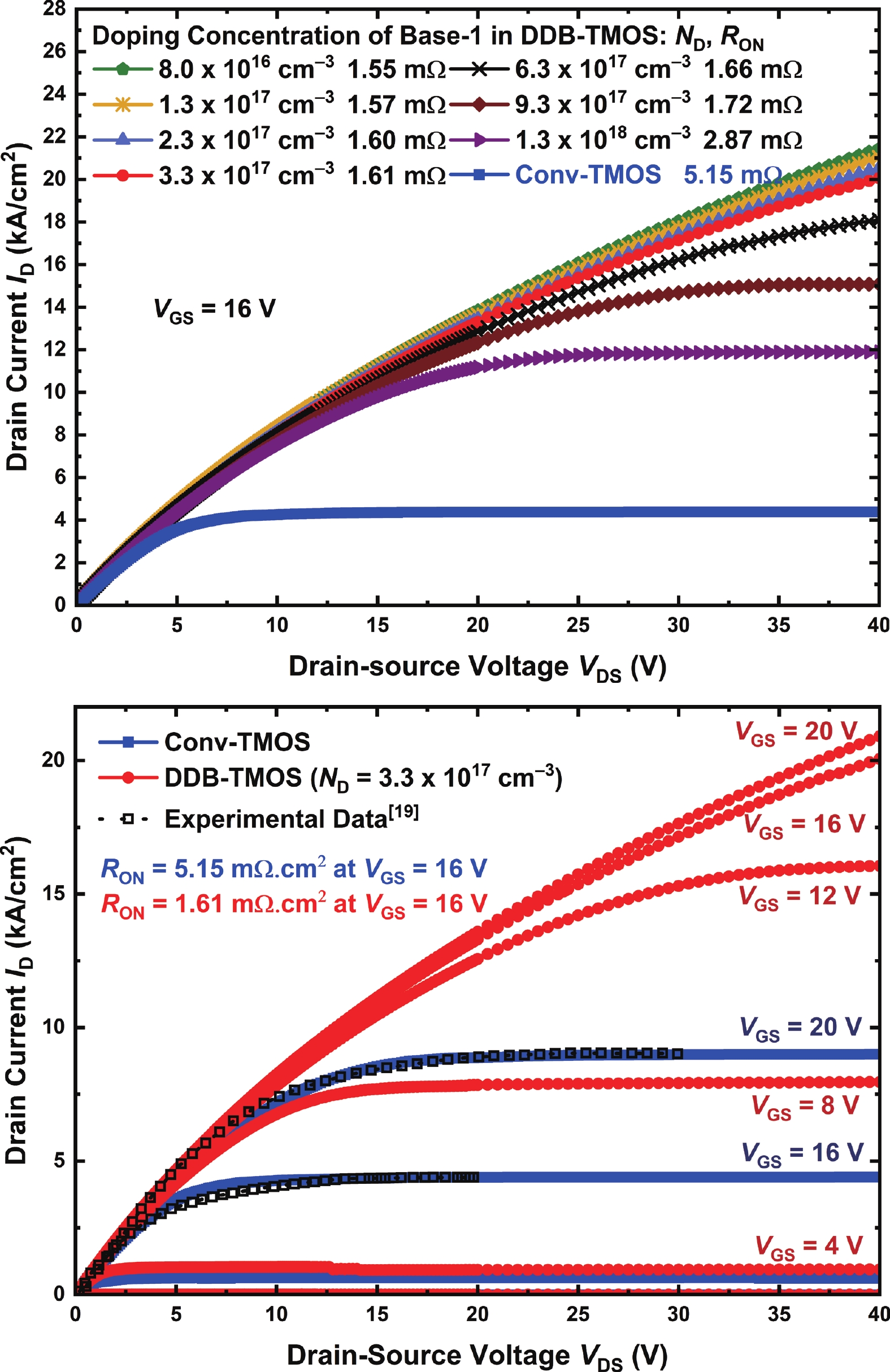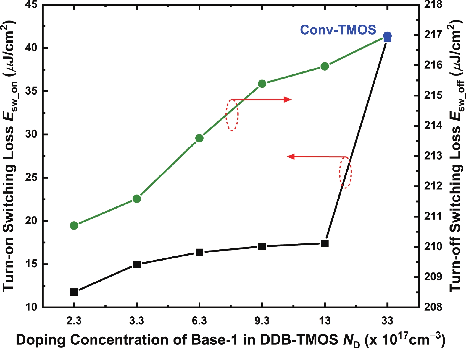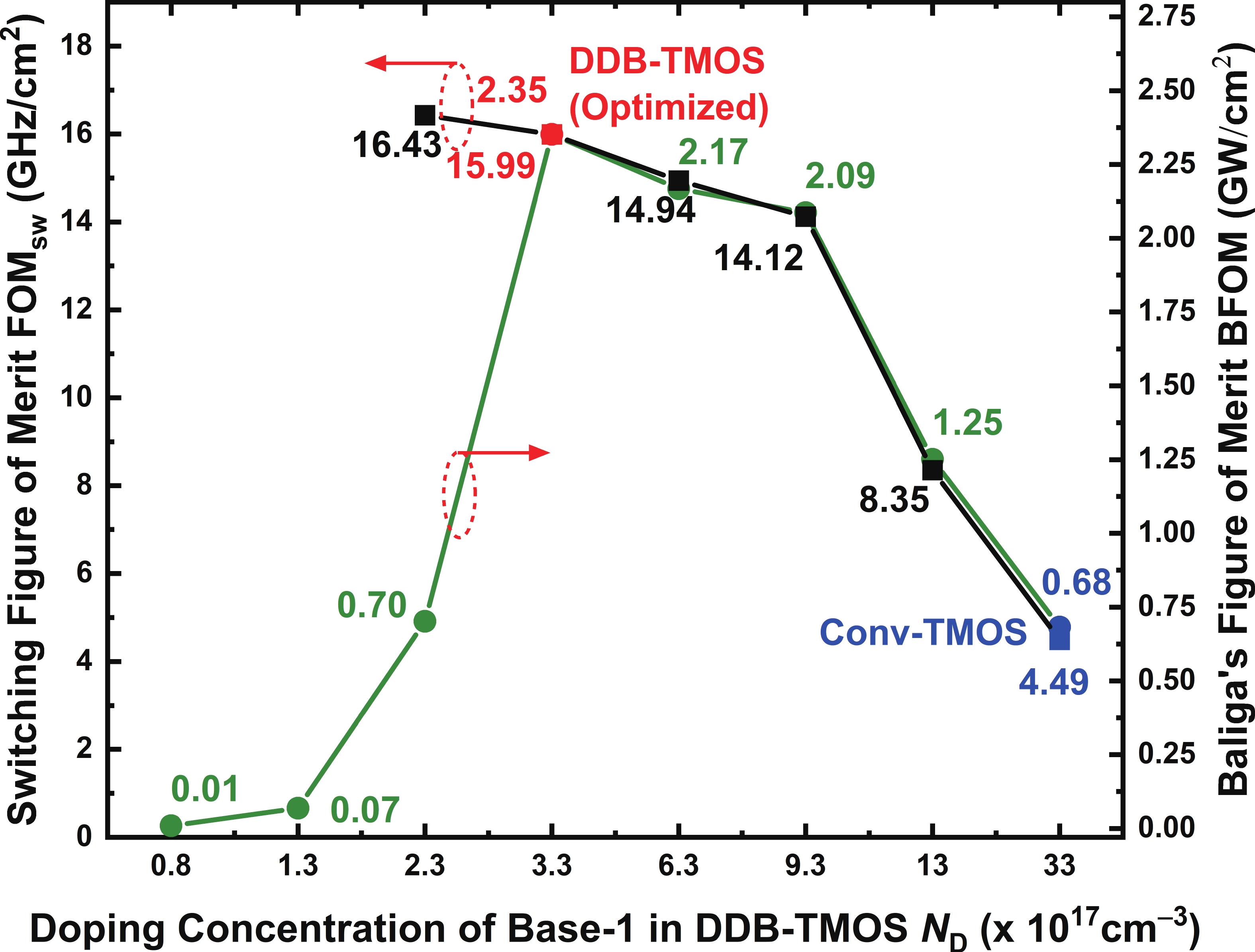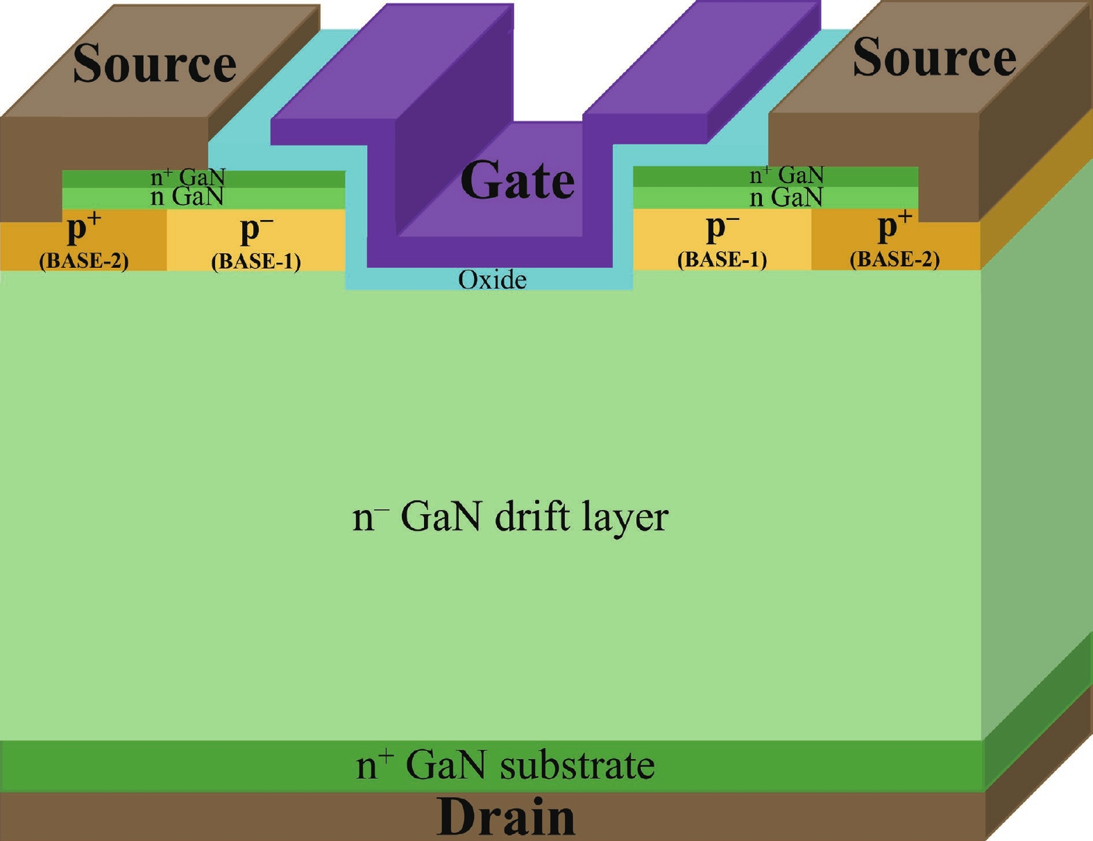
Fig. 1.
(Color online) Schematic of the Vertical GaN Double-Diffused Base trench MOSFET (DDB-TMOS).
ARTICLES
Ashrafun Naher Pinky1, Thomas Ebel1, Robert Plikat2 and Samaneh Sharbati1,
Corresponding author: Samaneh Sharbati, sharbati@sdu.dk
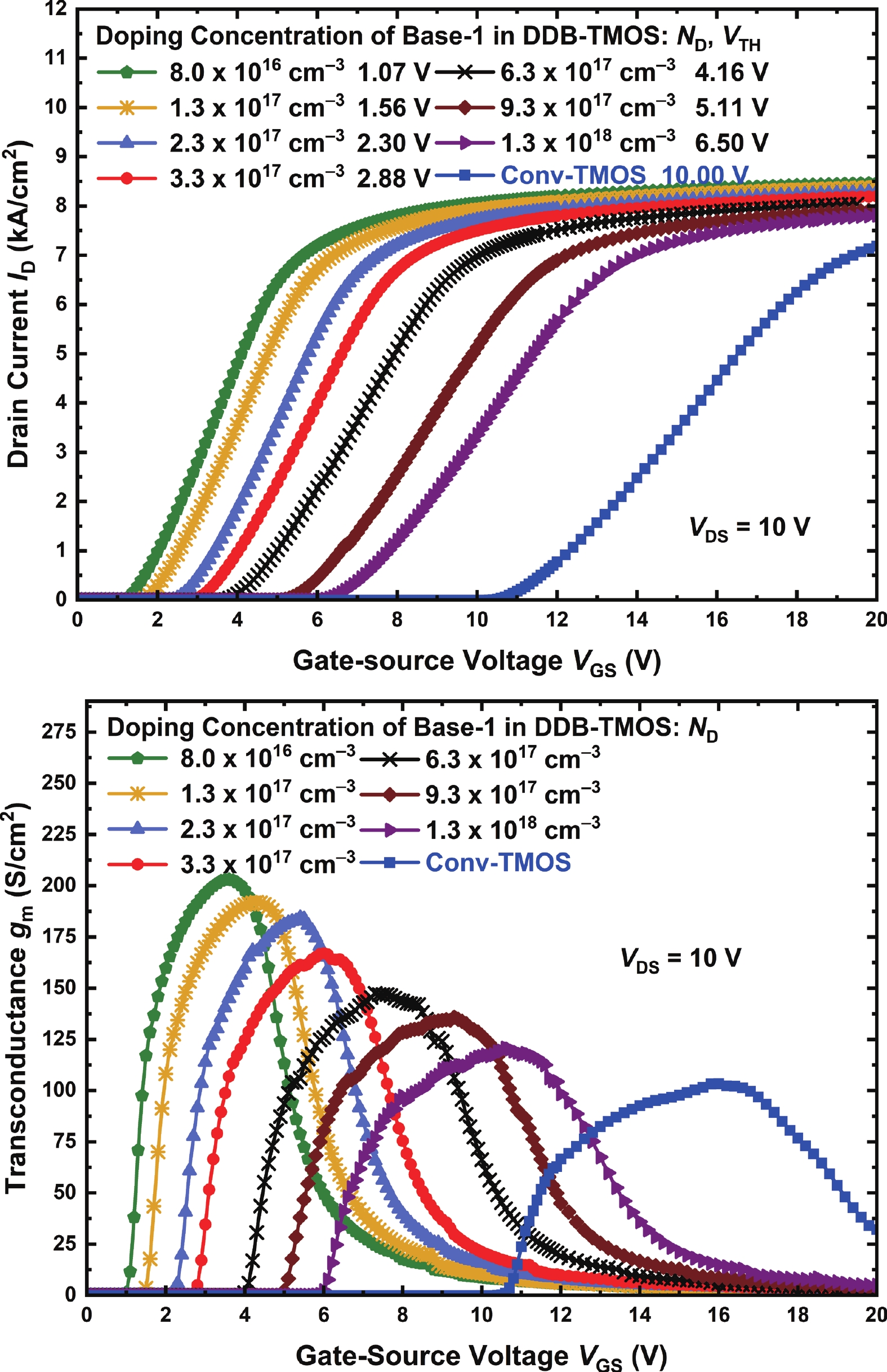
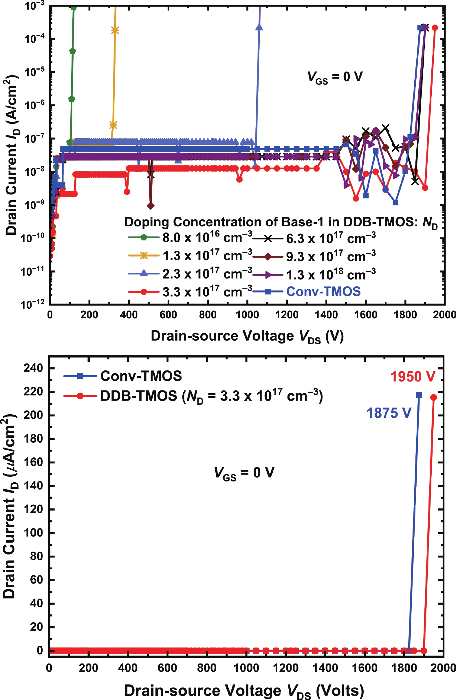
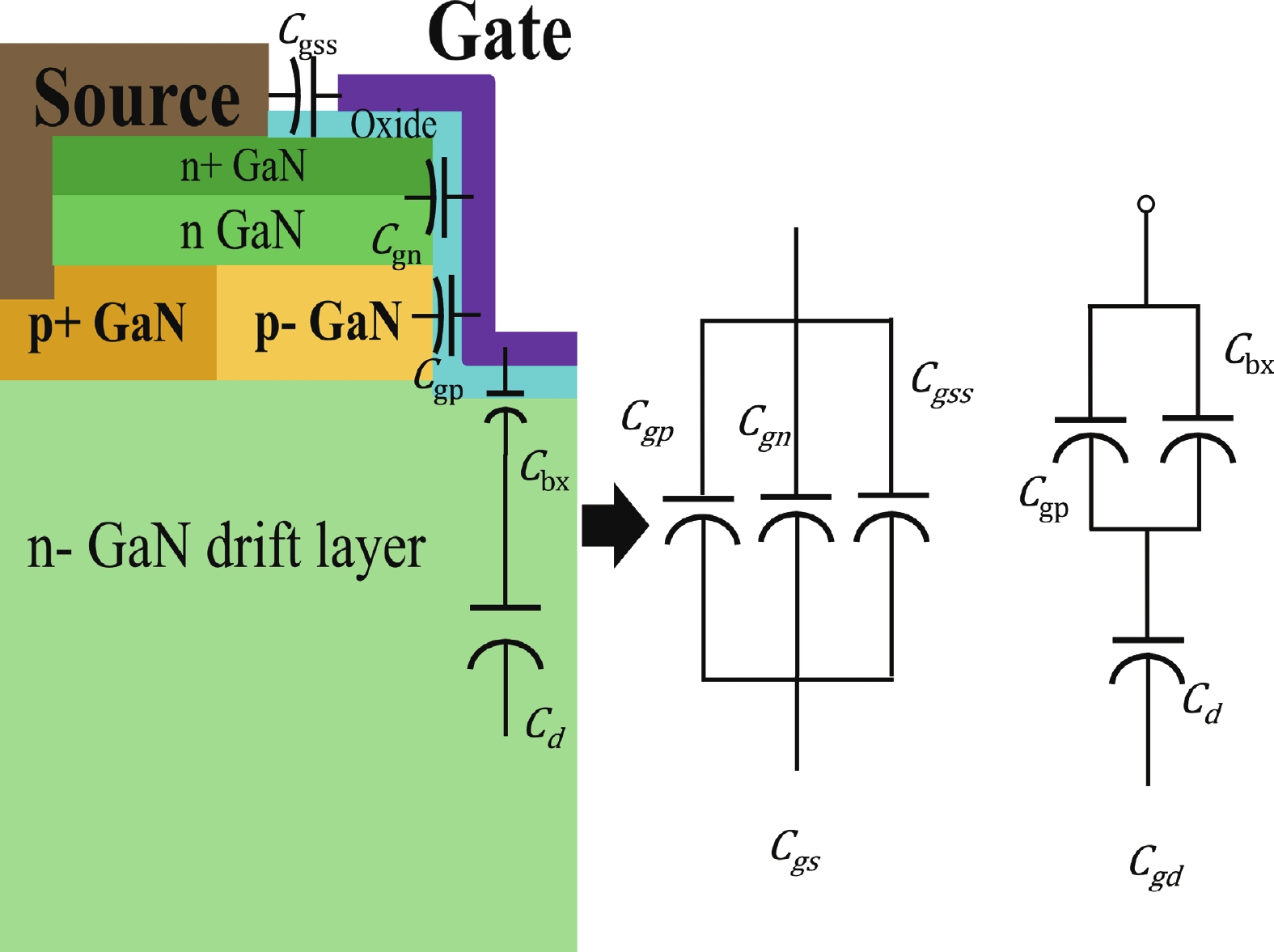
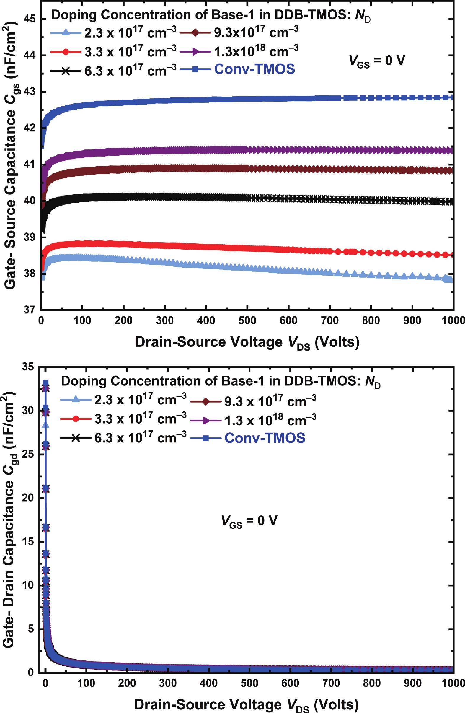
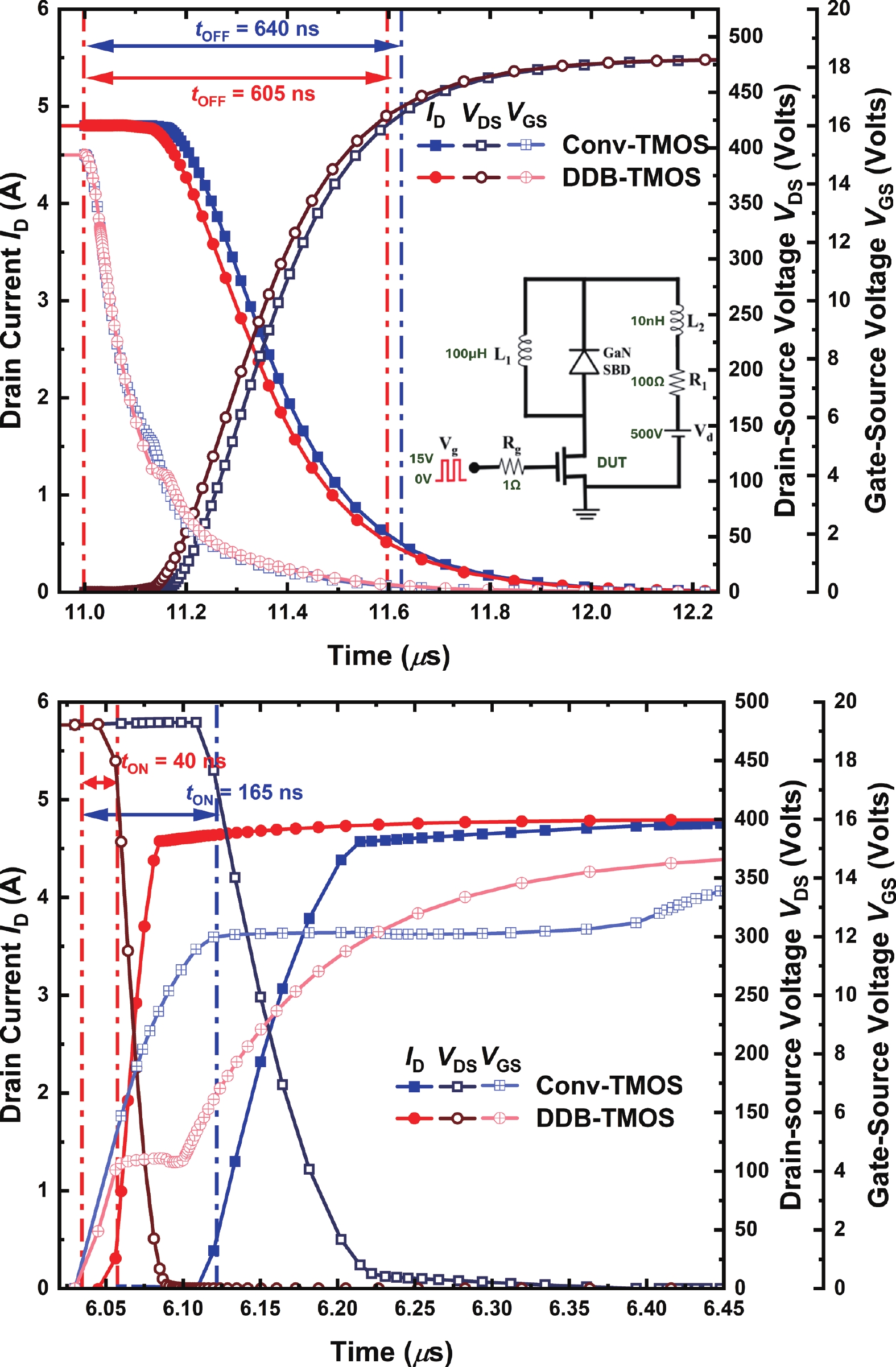
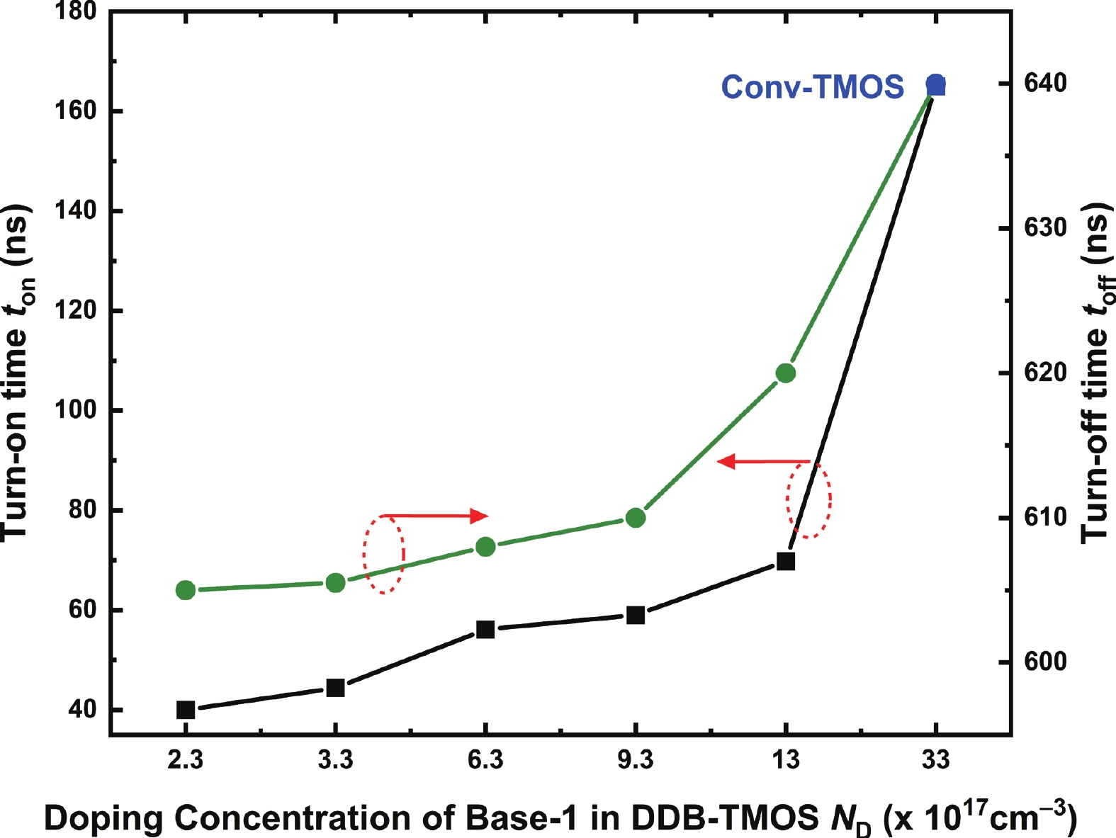
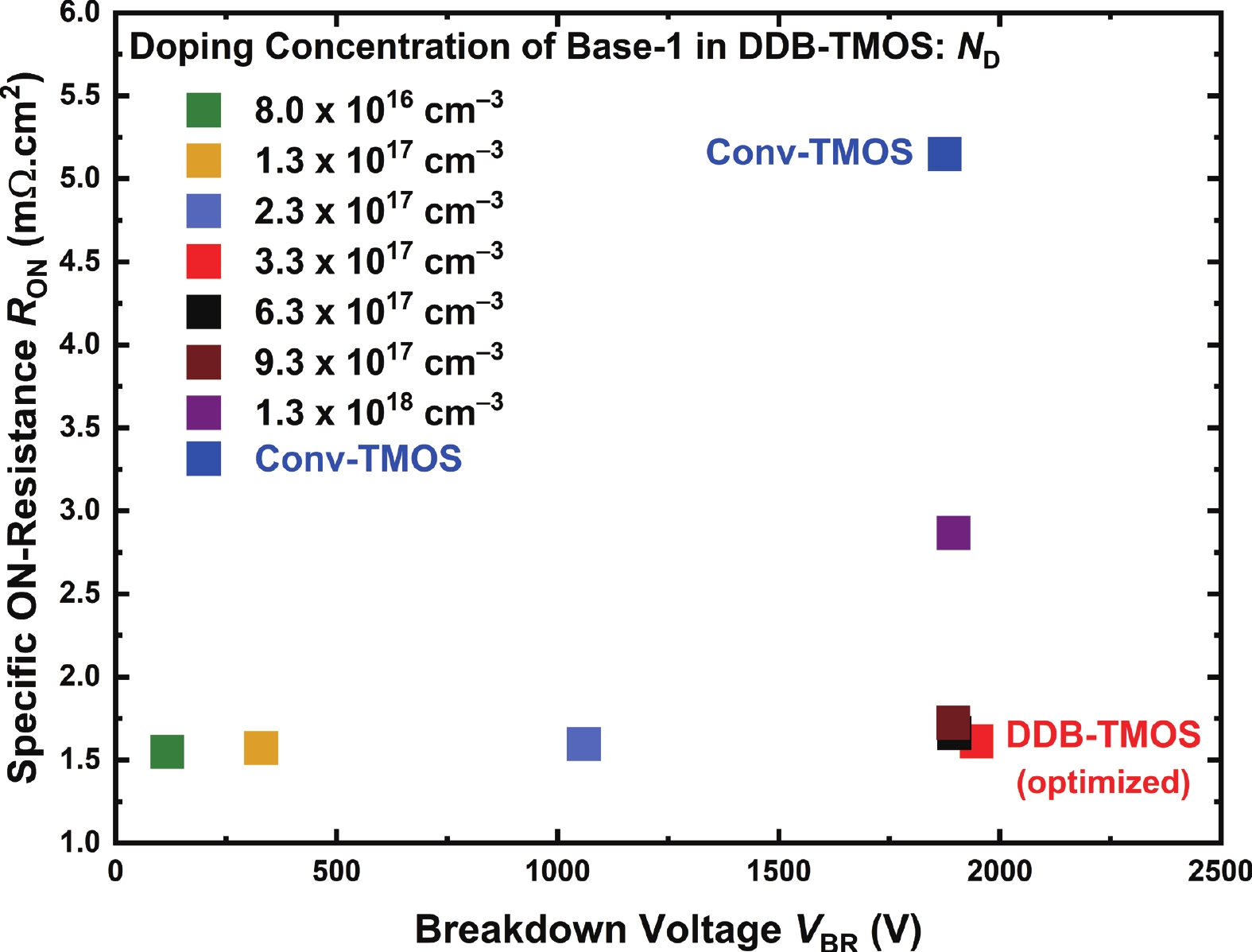
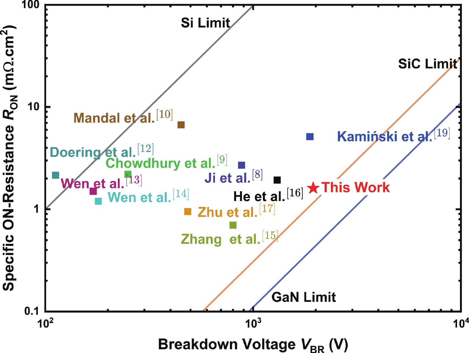
Abstract: This article presents the design of a Vertical GaN Trench MOSFET featuring a Double-Diffused Base (DDB-TMOS) with an in-depth analysis of its device physics. The introduction of a lightly doped p– GaN layer, where the channel forms, helps lower the potential barrier, improving electron transport from the n+ source into the n-drift region. The simulation study of the DDB-TMOS achieves a substantial reduction in threshold voltage from 10 V to 2.88 V, while the maximum current density increases from 9 kA/cm2 to 21 kA/cm2. As a result of structural optimization, the specific ON-resistance markedly decreases from 5.15 mΩ·cm2 to 1.61 mΩ·cm2. Additionally, the switching behavior of the device was systematically analyzed. The reduced base doping beneath the gate oxide led to a notable decrease in the gate-source capacitance by a factor of 1.2, decreasing the turn-on switching loss from 42 µJ/cm2 to 12 µJ/cm2. Following comprehensive static and dynamic analysis, the figure of merits (FOMs) were employed to optimize the device structure. The Baliga’s figure of merit increased from 0.68 to 2.35 GW/cm2, while the switching figure of merit improved from 4.49 to 16 GHz/cm2. This study confirms that the optimized DDB-TMOS is highly promising for future high-power switching applications.
Keywords: vertical GaN trench MOSFET, threshold voltage, specific ON-resistance, gate-source capacitance, switching loss
| [1] |
Meneghini M, De Santi C, Abid I, et al. GaN-based power devices: Physics, reliability, and perspectives. J Appl Phys, 2021, 130(18): 181101 doi: 10.1063/5.0061354
|
| [2] |
Sharbati S, Gharibshahian I, Ebel T, et al. Analytical model for two-dimensional electron gas charge density in recessed-gate GaN high-electron-mobility transistors. J Electron Mater, 2021, 50(7): 3923 doi: 10.1007/s11664-021-08842-7
|
| [3] |
Luan T T, Huang S, Jing G J, et al. Recess-free enhancement-mode AlGaN/GaN RF HEMTs on Si substrate. J Semicond, 2024, 45(6): 062301 doi: 10.1088/1674-4926/23120006
|
| [4] |
Meneghesso G, Verzellesi G, Danesin F, et al. Reliability of GaN high-electron-mobility transistors: State of the art and perspectives. IEEE Trans Device Mater Relib, 2008, 8(2): 332 doi: 10.1109/TDMR.2008.923743
|
| [5] |
Gill L, DasGupta S, Neely J C, et al. A review of GaN HEMT dynamic ON-resistance and dynamic stress effects on field distribution. IEEE Trans Power Electron, 2024, 39(1): 517 doi: 10.1109/TPEL.2023.3318182
|
| [6] |
Cioni M, Zagni N, Iucolano F, et al. Partial recovery of dynamic RON versus OFF-state stress voltage in p-GaN gate AlGaN/GaN power HEMTs. IEEE Trans Electron Devices, 2021, 68(10): 4862 doi: 10.1109/TED.2021.3105075
|
| [7] |
Zhu R P, Zhou Q, Tao H, et al. A split gate vertical GaN power transistor with intrinsic reverse conduction capability and low gate charge. 2018 IEEE 30th International Symposium on Power Semiconductor Devices and ICs (ISPSD), 2018: 212
|
| [8] |
Ji D, Agarwal A, Li H R, et al. 880 V/2.7 mΩ·cm2 MIS gate trench CAVET on bulk GaN substrates. IEEE Electron Device Lett, 2018, 39(6): 863 doi: 10.1109/LED.2018.2828844
|
| [9] |
Chowdhury S, Wong M H, Swenson B L, et al. CAVET on bulk GaN substrates achieved with MBE-regrown AlGaN/GaN layers to suppress dispersion. IEEE Electron Device Lett, 2012, 33(1): 41 doi: 10.1109/LED.2011.2173456
|
| [10] |
Mandal S, Agarwal A, Ahmadi E, et al. Dispersion free 450-V p GaN-gated CAVETs with Mg-ion implanted blocking layer. IEEE Electron Device Lett, 2017, 38(7): 933 doi: 10.1109/LED.2017.2709940
|
| [11] |
Zagni N, Fregolent M, Del Fiol A, et al. Physical insights into trapping effects on vertical GaN-on-Si trench MOSFETs from TCAD. J Semicond, 2024, 45(3): 032501 doi: 10.1088/1674-4926/45/3/032501
|
| [12] |
Doering P, Driad R, Reiner R, et al. Metal organic chemical vapour deposition regrown large area GaN-on-GaN current aperture vertical electron transistors with high current capability. Electron Lett, 2021, 57(3): 145 doi: 10.1049/ell2.12068
|
| [13] |
Wen X Y, Lee K J, Nakazato Y, et al. High current density trench CAVET on bulk GaN substrates with low-temperature GaN suppressing Mg diffusion. Crystals, 2023, 13(4): 709 doi: 10.3390/cryst13040709
|
| [14] |
Wen X Y, Shankar B, Lee K, et al. 10 MHz-switching on GaN trench CAVET up to 300 °C operation enabled by high channel mobility. IEEE Electron Device Lett, 2024, 45(4): 653 doi: 10.1109/LED.2024.3360917
|
| [15] |
Zhang R Z, Liu J C, Li Q, et al. Breakthrough short circuit robustness demonstrated in vertical GaN fin JFET. IEEE Trans Power Electron, 2022, 37(6): 6253 doi: 10.1109/TPEL.2021.3138451
|
| [16] |
He W, Li J, Liao Z L, et al. 1.3kV vertical GaN-based trench MOSFETs on 4-inch free standing GaN wafer. Nanoscale Res Lett, 2022, 17(1): 14 doi: 10.1186/s11671-022-03653-z
|
| [17] |
Zhu R Q, Jiang H X, Tang C W, et al. Enhancing ON- and OFF-state performance of quasi-vertical GaN trench MOSFETs on sapphire with reduced interface charges and a thick bottom dielectric. IEEE Electron Device Lett, 2022, 43(3): 346 doi: 10.1109/LED.2022.3146276
|
| [18] |
Jaiswal N K, Ramakrishnan V N. An optimized vertical GaN parallel split gate trench MOSFET device structure for improved switching performance. IEEE Access, 2023, 11: 46998 doi: 10.1109/ACCESS.2023.3265477
|
| [19] |
Kamiński M, Taube A, Tarenko J, et al. Vertical GaN trench-MOSFETs fabricated on ammonothermally grown bulk GaN substrates. Phys Status Solidi A, 2024, 221(21): 2400077 doi: 10.1002/pssa.202400077
|
| [20] |
Jaiswal N K, Ebel T, Sharbati S. Enhancing DC-DC boost converter performance with vertical GaN split-RSO-MOSFET. PCIM Conference 2025; International Exhibition and Conference for Power Electronics, Intelligent Motion, Renewable Energy and Energy Management. Nürnberg, Germany. VDE, 2025: 1626
|
| [21] |
Pinky A N, Ebel T, Sharbati S. Design approach for lateral optimization of GaN CAVETs: A static characteristics study. Power Electron Devices Compon, 2025, 10: 100075 doi: 10.1016/j.pedc.2024.100075
|
| [22] |
Pinky A N, Ebel T, Sharbati S. Optimization of current aperture length for enhanced RF performance in GaN CAVET devices. PCIM Conference 2025; International Exhibition and Conference for Power Electronics, Intelligent Motion, Renewable Energy and Energy Management. Nürnberg, Germany. VDE, 2025: 1632
|
| [23] |
Pinky A N, Ebel T, Plikat R, et al. A comprehensive analysis of GaN CAVET for power-switching applications. 2025 Energy Conversion Congress & Expo Europe (ECCE Europe). Birmingham, United Kingdom. IEEE, 2025: 1
|
| [24] |
Williams R K, Darwish M N, Blanchard R A, et al. The trench power MOSFET: Part I: History, technology, and prospects. IEEE Trans Electron Devices, 2017, 64(3): 674 doi: 10.1109/TED.2017.2653239
|
| [25] |
Liu S, Song X F, Zhang J C, et al. Comprehensive design of device parameters for GaN vertical trench MOSFETs. IEEE Access, 2020, 8: 57126 doi: 10.1109/ACCESS.2020.2977381
|
| [26] |
Qiu Y H, Wei L. The GaN trench MOSFET with adaptive voltage tolerance achieved through a dual-shielding structure. Semicond Sci Technol, 2024, 39(5): 055004 doi: 10.1088/1361-6641/ad3274
|
| [27] |
Sabui G, Parbrook P J, Arredondo-Arechavala M, et al. Modeling and simulation of bulk gallium nitride power semiconductor devices. AIP Adv, 2016, 6(5): 055006 doi: 10.1063/1.4948794
|
| [28] |
Prasad C V, Dharmaiah P, Lee G H, et al. Interface engineering of 4H-SiC-based UV photodetectors: A comprehensive review. Mater Today Adv, 2025, 28: 100662 doi: 10.1016/j.mtadv.2025.100662
|
| [29] |
Dharmawardana K G P, Amaratunga G A J. Modeling of high current density trench gate MOSFET. IEEE Trans Electron Devices, 2000, 47(12): 2420 doi: 10.1109/16.887031
|
| [30] |
Otake H, Chikamatsu K, Yamaguchi A, et al. Vertical GaN-based trench gate metal oxide semiconductor field-effect transistors on GaN bulk substrates. Appl Phys Express, 2008, 1(1): 011105 doi: 10.1143/APEX.1.011105
|
| [31] |
Sun S C, Plummer J D. Modeling of the on-resistance of LDMOS, VDMOS, and VMOS power transistors. IEEE Trans Electron Devices, 1980, 27(2): 356 doi: 10.1109/T-ED.1980.19868
|
| [32] |
Li S, Liu S Y, Tian Y, et al. High-temperature electrical performances and physics-based analysis of p-GaN HEMT device. IET Power Electron, 2020, 13(3): 420 doi: 10.1049/iet-pel.2019.0510
|
| [1] |
Meneghini M, De Santi C, Abid I, et al. GaN-based power devices: Physics, reliability, and perspectives. J Appl Phys, 2021, 130(18): 181101 doi: 10.1063/5.0061354
|
| [2] |
Sharbati S, Gharibshahian I, Ebel T, et al. Analytical model for two-dimensional electron gas charge density in recessed-gate GaN high-electron-mobility transistors. J Electron Mater, 2021, 50(7): 3923 doi: 10.1007/s11664-021-08842-7
|
| [3] |
Luan T T, Huang S, Jing G J, et al. Recess-free enhancement-mode AlGaN/GaN RF HEMTs on Si substrate. J Semicond, 2024, 45(6): 062301 doi: 10.1088/1674-4926/23120006
|
| [4] |
Meneghesso G, Verzellesi G, Danesin F, et al. Reliability of GaN high-electron-mobility transistors: State of the art and perspectives. IEEE Trans Device Mater Relib, 2008, 8(2): 332 doi: 10.1109/TDMR.2008.923743
|
| [5] |
Gill L, DasGupta S, Neely J C, et al. A review of GaN HEMT dynamic ON-resistance and dynamic stress effects on field distribution. IEEE Trans Power Electron, 2024, 39(1): 517 doi: 10.1109/TPEL.2023.3318182
|
| [6] |
Cioni M, Zagni N, Iucolano F, et al. Partial recovery of dynamic RON versus OFF-state stress voltage in p-GaN gate AlGaN/GaN power HEMTs. IEEE Trans Electron Devices, 2021, 68(10): 4862 doi: 10.1109/TED.2021.3105075
|
| [7] |
Zhu R P, Zhou Q, Tao H, et al. A split gate vertical GaN power transistor with intrinsic reverse conduction capability and low gate charge. 2018 IEEE 30th International Symposium on Power Semiconductor Devices and ICs (ISPSD), 2018: 212
|
| [8] |
Ji D, Agarwal A, Li H R, et al. 880 V/2.7 mΩ·cm2 MIS gate trench CAVET on bulk GaN substrates. IEEE Electron Device Lett, 2018, 39(6): 863 doi: 10.1109/LED.2018.2828844
|
| [9] |
Chowdhury S, Wong M H, Swenson B L, et al. CAVET on bulk GaN substrates achieved with MBE-regrown AlGaN/GaN layers to suppress dispersion. IEEE Electron Device Lett, 2012, 33(1): 41 doi: 10.1109/LED.2011.2173456
|
| [10] |
Mandal S, Agarwal A, Ahmadi E, et al. Dispersion free 450-V p GaN-gated CAVETs with Mg-ion implanted blocking layer. IEEE Electron Device Lett, 2017, 38(7): 933 doi: 10.1109/LED.2017.2709940
|
| [11] |
Zagni N, Fregolent M, Del Fiol A, et al. Physical insights into trapping effects on vertical GaN-on-Si trench MOSFETs from TCAD. J Semicond, 2024, 45(3): 032501 doi: 10.1088/1674-4926/45/3/032501
|
| [12] |
Doering P, Driad R, Reiner R, et al. Metal organic chemical vapour deposition regrown large area GaN-on-GaN current aperture vertical electron transistors with high current capability. Electron Lett, 2021, 57(3): 145 doi: 10.1049/ell2.12068
|
| [13] |
Wen X Y, Lee K J, Nakazato Y, et al. High current density trench CAVET on bulk GaN substrates with low-temperature GaN suppressing Mg diffusion. Crystals, 2023, 13(4): 709 doi: 10.3390/cryst13040709
|
| [14] |
Wen X Y, Shankar B, Lee K, et al. 10 MHz-switching on GaN trench CAVET up to 300 °C operation enabled by high channel mobility. IEEE Electron Device Lett, 2024, 45(4): 653 doi: 10.1109/LED.2024.3360917
|
| [15] |
Zhang R Z, Liu J C, Li Q, et al. Breakthrough short circuit robustness demonstrated in vertical GaN fin JFET. IEEE Trans Power Electron, 2022, 37(6): 6253 doi: 10.1109/TPEL.2021.3138451
|
| [16] |
He W, Li J, Liao Z L, et al. 1.3kV vertical GaN-based trench MOSFETs on 4-inch free standing GaN wafer. Nanoscale Res Lett, 2022, 17(1): 14 doi: 10.1186/s11671-022-03653-z
|
| [17] |
Zhu R Q, Jiang H X, Tang C W, et al. Enhancing ON- and OFF-state performance of quasi-vertical GaN trench MOSFETs on sapphire with reduced interface charges and a thick bottom dielectric. IEEE Electron Device Lett, 2022, 43(3): 346 doi: 10.1109/LED.2022.3146276
|
| [18] |
Jaiswal N K, Ramakrishnan V N. An optimized vertical GaN parallel split gate trench MOSFET device structure for improved switching performance. IEEE Access, 2023, 11: 46998 doi: 10.1109/ACCESS.2023.3265477
|
| [19] |
Kamiński M, Taube A, Tarenko J, et al. Vertical GaN trench-MOSFETs fabricated on ammonothermally grown bulk GaN substrates. Phys Status Solidi A, 2024, 221(21): 2400077 doi: 10.1002/pssa.202400077
|
| [20] |
Jaiswal N K, Ebel T, Sharbati S. Enhancing DC-DC boost converter performance with vertical GaN split-RSO-MOSFET. PCIM Conference 2025; International Exhibition and Conference for Power Electronics, Intelligent Motion, Renewable Energy and Energy Management. Nürnberg, Germany. VDE, 2025: 1626
|
| [21] |
Pinky A N, Ebel T, Sharbati S. Design approach for lateral optimization of GaN CAVETs: A static characteristics study. Power Electron Devices Compon, 2025, 10: 100075 doi: 10.1016/j.pedc.2024.100075
|
| [22] |
Pinky A N, Ebel T, Sharbati S. Optimization of current aperture length for enhanced RF performance in GaN CAVET devices. PCIM Conference 2025; International Exhibition and Conference for Power Electronics, Intelligent Motion, Renewable Energy and Energy Management. Nürnberg, Germany. VDE, 2025: 1632
|
| [23] |
Pinky A N, Ebel T, Plikat R, et al. A comprehensive analysis of GaN CAVET for power-switching applications. 2025 Energy Conversion Congress & Expo Europe (ECCE Europe). Birmingham, United Kingdom. IEEE, 2025: 1
|
| [24] |
Williams R K, Darwish M N, Blanchard R A, et al. The trench power MOSFET: Part I: History, technology, and prospects. IEEE Trans Electron Devices, 2017, 64(3): 674 doi: 10.1109/TED.2017.2653239
|
| [25] |
Liu S, Song X F, Zhang J C, et al. Comprehensive design of device parameters for GaN vertical trench MOSFETs. IEEE Access, 2020, 8: 57126 doi: 10.1109/ACCESS.2020.2977381
|
| [26] |
Qiu Y H, Wei L. The GaN trench MOSFET with adaptive voltage tolerance achieved through a dual-shielding structure. Semicond Sci Technol, 2024, 39(5): 055004 doi: 10.1088/1361-6641/ad3274
|
| [27] |
Sabui G, Parbrook P J, Arredondo-Arechavala M, et al. Modeling and simulation of bulk gallium nitride power semiconductor devices. AIP Adv, 2016, 6(5): 055006 doi: 10.1063/1.4948794
|
| [28] |
Prasad C V, Dharmaiah P, Lee G H, et al. Interface engineering of 4H-SiC-based UV photodetectors: A comprehensive review. Mater Today Adv, 2025, 28: 100662 doi: 10.1016/j.mtadv.2025.100662
|
| [29] |
Dharmawardana K G P, Amaratunga G A J. Modeling of high current density trench gate MOSFET. IEEE Trans Electron Devices, 2000, 47(12): 2420 doi: 10.1109/16.887031
|
| [30] |
Otake H, Chikamatsu K, Yamaguchi A, et al. Vertical GaN-based trench gate metal oxide semiconductor field-effect transistors on GaN bulk substrates. Appl Phys Express, 2008, 1(1): 011105 doi: 10.1143/APEX.1.011105
|
| [31] |
Sun S C, Plummer J D. Modeling of the on-resistance of LDMOS, VDMOS, and VMOS power transistors. IEEE Trans Electron Devices, 1980, 27(2): 356 doi: 10.1109/T-ED.1980.19868
|
| [32] |
Li S, Liu S Y, Tian Y, et al. High-temperature electrical performances and physics-based analysis of p-GaN HEMT device. IET Power Electron, 2020, 13(3): 420 doi: 10.1049/iet-pel.2019.0510
|





Article views: 47 Times PDF downloads: 58 Times Cited by: 0 Times
Received: 17 November 2025 Revised: 01 June 2026 Online: Accepted Manuscript: 10 September 2026
| Citation: |
Ashrafun Naher Pinky, Thomas Ebel, Robert Plikat, Samaneh Sharbati. Design and optimization of vertical GaN double-diffused base MOSFET enabling high-power switching[J]. Journal of Semiconductors, 2026, In Press. doi: 10.1088/1674-4926/25110014
****
A N Pinky, T Ebel, R Plikat, and S Sharbati, Design and optimization of vertical GaN double-diffused base MOSFET enabling high-power switching[J]. J. Semicond., 2026, accepted doi: 10.1088/1674-4926/25110014

|
 Ashrafun Naher Pinky is currently pursuing a PhD at the Centre for Industrial Electronics (CIE) at the University of Southern Denmark (SDU), focusing on the design of fast-switching vertical GaN power devices. She received her B.Sc. and M.Sc. degrees in electrical and electronic engineering from Rajshahi University of Engineering and Technology, Bangladesh. Her research interests include high-efficiency devices for power electronics applications, in particular improving breakdown voltage and Figure of Merit in vertical GaN devices
 Dr. Thomas Ebel is Professor and Head of Electrical Engineering and the Centre for Industrial Electronics at the University of Southern Denmark. He has extensive industrial and academic leadership experience in power electronics, capacitors, magnetics, electrolyzers, reliability, and AI-based condition monitoring. He has led numerous national and international research projects and currently supervises PhD students and postdoctoral researchers. His scientific output includes 208 publications, 14 patents, and more than 1,500 citations. He received SDU’s TEK Innovation Prize in 2023
 Robert Plikat (M’96) received the Dipl.-Ing. degree in electrical engineering and the Dr.-Ing. (Ph.D.) degree from the University of Bremen, Bremen, Germany, in 1994 and 2000, respectively. He has over 15 years of experience in automotive research and development. He is currently with Powertrain Systems, Group Research, Volkswagen AG, Wolfsburg, Germany. His current research interests include the electrification of vehicles, the respective components, and the related technologies, in particular, power electronics and drives
 Samaneh Sharbati is working as an associate professor at the Centre for Industrial Electronics (CIE) at the University of Southern Denmark (SDU) for the past 6 years. Her research interests include Semiconductor Devices, focusing on GaN Devices. She received the B.Sc. and M.S. degrees in electronic engineering from Semnan University, Semnan, Iran, in 2001 and 2006, and a Ph.D. from Ferdowsi University of Mashhad, Mashhad, Iran, in 2015. She has published more than 30 research papers
| [1] |
Meneghini M, De Santi C, Abid I, et al. GaN-based power devices: Physics, reliability, and perspectives. J Appl Phys, 2021, 130(18): 181101 doi: 10.1063/5.0061354
|
| [2] |
Sharbati S, Gharibshahian I, Ebel T, et al. Analytical model for two-dimensional electron gas charge density in recessed-gate GaN high-electron-mobility transistors. J Electron Mater, 2021, 50(7): 3923 doi: 10.1007/s11664-021-08842-7
|
| [3] |
Luan T T, Huang S, Jing G J, et al. Recess-free enhancement-mode AlGaN/GaN RF HEMTs on Si substrate. J Semicond, 2024, 45(6): 062301 doi: 10.1088/1674-4926/23120006
|
| [4] |
Meneghesso G, Verzellesi G, Danesin F, et al. Reliability of GaN high-electron-mobility transistors: State of the art and perspectives. IEEE Trans Device Mater Relib, 2008, 8(2): 332 doi: 10.1109/TDMR.2008.923743
|
| [5] |
Gill L, DasGupta S, Neely J C, et al. A review of GaN HEMT dynamic ON-resistance and dynamic stress effects on field distribution. IEEE Trans Power Electron, 2024, 39(1): 517 doi: 10.1109/TPEL.2023.3318182
|
| [6] |
Cioni M, Zagni N, Iucolano F, et al. Partial recovery of dynamic RON versus OFF-state stress voltage in p-GaN gate AlGaN/GaN power HEMTs. IEEE Trans Electron Devices, 2021, 68(10): 4862 doi: 10.1109/TED.2021.3105075
|
| [7] |
Zhu R P, Zhou Q, Tao H, et al. A split gate vertical GaN power transistor with intrinsic reverse conduction capability and low gate charge. 2018 IEEE 30th International Symposium on Power Semiconductor Devices and ICs (ISPSD), 2018: 212
|
| [8] |
Ji D, Agarwal A, Li H R, et al. 880 V/2.7 mΩ·cm2 MIS gate trench CAVET on bulk GaN substrates. IEEE Electron Device Lett, 2018, 39(6): 863 doi: 10.1109/LED.2018.2828844
|
| [9] |
Chowdhury S, Wong M H, Swenson B L, et al. CAVET on bulk GaN substrates achieved with MBE-regrown AlGaN/GaN layers to suppress dispersion. IEEE Electron Device Lett, 2012, 33(1): 41 doi: 10.1109/LED.2011.2173456
|
| [10] |
Mandal S, Agarwal A, Ahmadi E, et al. Dispersion free 450-V p GaN-gated CAVETs with Mg-ion implanted blocking layer. IEEE Electron Device Lett, 2017, 38(7): 933 doi: 10.1109/LED.2017.2709940
|
| [11] |
Zagni N, Fregolent M, Del Fiol A, et al. Physical insights into trapping effects on vertical GaN-on-Si trench MOSFETs from TCAD. J Semicond, 2024, 45(3): 032501 doi: 10.1088/1674-4926/45/3/032501
|
| [12] |
Doering P, Driad R, Reiner R, et al. Metal organic chemical vapour deposition regrown large area GaN-on-GaN current aperture vertical electron transistors with high current capability. Electron Lett, 2021, 57(3): 145 doi: 10.1049/ell2.12068
|
| [13] |
Wen X Y, Lee K J, Nakazato Y, et al. High current density trench CAVET on bulk GaN substrates with low-temperature GaN suppressing Mg diffusion. Crystals, 2023, 13(4): 709 doi: 10.3390/cryst13040709
|
| [14] |
Wen X Y, Shankar B, Lee K, et al. 10 MHz-switching on GaN trench CAVET up to 300 °C operation enabled by high channel mobility. IEEE Electron Device Lett, 2024, 45(4): 653 doi: 10.1109/LED.2024.3360917
|
| [15] |
Zhang R Z, Liu J C, Li Q, et al. Breakthrough short circuit robustness demonstrated in vertical GaN fin JFET. IEEE Trans Power Electron, 2022, 37(6): 6253 doi: 10.1109/TPEL.2021.3138451
|
| [16] |
He W, Li J, Liao Z L, et al. 1.3kV vertical GaN-based trench MOSFETs on 4-inch free standing GaN wafer. Nanoscale Res Lett, 2022, 17(1): 14 doi: 10.1186/s11671-022-03653-z
|
| [17] |
Zhu R Q, Jiang H X, Tang C W, et al. Enhancing ON- and OFF-state performance of quasi-vertical GaN trench MOSFETs on sapphire with reduced interface charges and a thick bottom dielectric. IEEE Electron Device Lett, 2022, 43(3): 346 doi: 10.1109/LED.2022.3146276
|
| [18] |
Jaiswal N K, Ramakrishnan V N. An optimized vertical GaN parallel split gate trench MOSFET device structure for improved switching performance. IEEE Access, 2023, 11: 46998 doi: 10.1109/ACCESS.2023.3265477
|
| [19] |
Kamiński M, Taube A, Tarenko J, et al. Vertical GaN trench-MOSFETs fabricated on ammonothermally grown bulk GaN substrates. Phys Status Solidi A, 2024, 221(21): 2400077 doi: 10.1002/pssa.202400077
|
| [20] |
Jaiswal N K, Ebel T, Sharbati S. Enhancing DC-DC boost converter performance with vertical GaN split-RSO-MOSFET. PCIM Conference 2025; International Exhibition and Conference for Power Electronics, Intelligent Motion, Renewable Energy and Energy Management. Nürnberg, Germany. VDE, 2025: 1626
|
| [21] |
Pinky A N, Ebel T, Sharbati S. Design approach for lateral optimization of GaN CAVETs: A static characteristics study. Power Electron Devices Compon, 2025, 10: 100075 doi: 10.1016/j.pedc.2024.100075
|
| [22] |
Pinky A N, Ebel T, Sharbati S. Optimization of current aperture length for enhanced RF performance in GaN CAVET devices. PCIM Conference 2025; International Exhibition and Conference for Power Electronics, Intelligent Motion, Renewable Energy and Energy Management. Nürnberg, Germany. VDE, 2025: 1632
|
| [23] |
Pinky A N, Ebel T, Plikat R, et al. A comprehensive analysis of GaN CAVET for power-switching applications. 2025 Energy Conversion Congress & Expo Europe (ECCE Europe). Birmingham, United Kingdom. IEEE, 2025: 1
|
| [24] |
Williams R K, Darwish M N, Blanchard R A, et al. The trench power MOSFET: Part I: History, technology, and prospects. IEEE Trans Electron Devices, 2017, 64(3): 674 doi: 10.1109/TED.2017.2653239
|
| [25] |
Liu S, Song X F, Zhang J C, et al. Comprehensive design of device parameters for GaN vertical trench MOSFETs. IEEE Access, 2020, 8: 57126 doi: 10.1109/ACCESS.2020.2977381
|
| [26] |
Qiu Y H, Wei L. The GaN trench MOSFET with adaptive voltage tolerance achieved through a dual-shielding structure. Semicond Sci Technol, 2024, 39(5): 055004 doi: 10.1088/1361-6641/ad3274
|
| [27] |
Sabui G, Parbrook P J, Arredondo-Arechavala M, et al. Modeling and simulation of bulk gallium nitride power semiconductor devices. AIP Adv, 2016, 6(5): 055006 doi: 10.1063/1.4948794
|
| [28] |
Prasad C V, Dharmaiah P, Lee G H, et al. Interface engineering of 4H-SiC-based UV photodetectors: A comprehensive review. Mater Today Adv, 2025, 28: 100662 doi: 10.1016/j.mtadv.2025.100662
|
| [29] |
Dharmawardana K G P, Amaratunga G A J. Modeling of high current density trench gate MOSFET. IEEE Trans Electron Devices, 2000, 47(12): 2420 doi: 10.1109/16.887031
|
| [30] |
Otake H, Chikamatsu K, Yamaguchi A, et al. Vertical GaN-based trench gate metal oxide semiconductor field-effect transistors on GaN bulk substrates. Appl Phys Express, 2008, 1(1): 011105 doi: 10.1143/APEX.1.011105
|
| [31] |
Sun S C, Plummer J D. Modeling of the on-resistance of LDMOS, VDMOS, and VMOS power transistors. IEEE Trans Electron Devices, 1980, 27(2): 356 doi: 10.1109/T-ED.1980.19868
|
| [32] |
Li S, Liu S Y, Tian Y, et al. High-temperature electrical performances and physics-based analysis of p-GaN HEMT device. IET Power Electron, 2020, 13(3): 420 doi: 10.1049/iet-pel.2019.0510
|

 WeChat ID
Journal of Semiconductors © 2017 All Rights Reserved 京ICP备05085259号-2

 DownLoad: