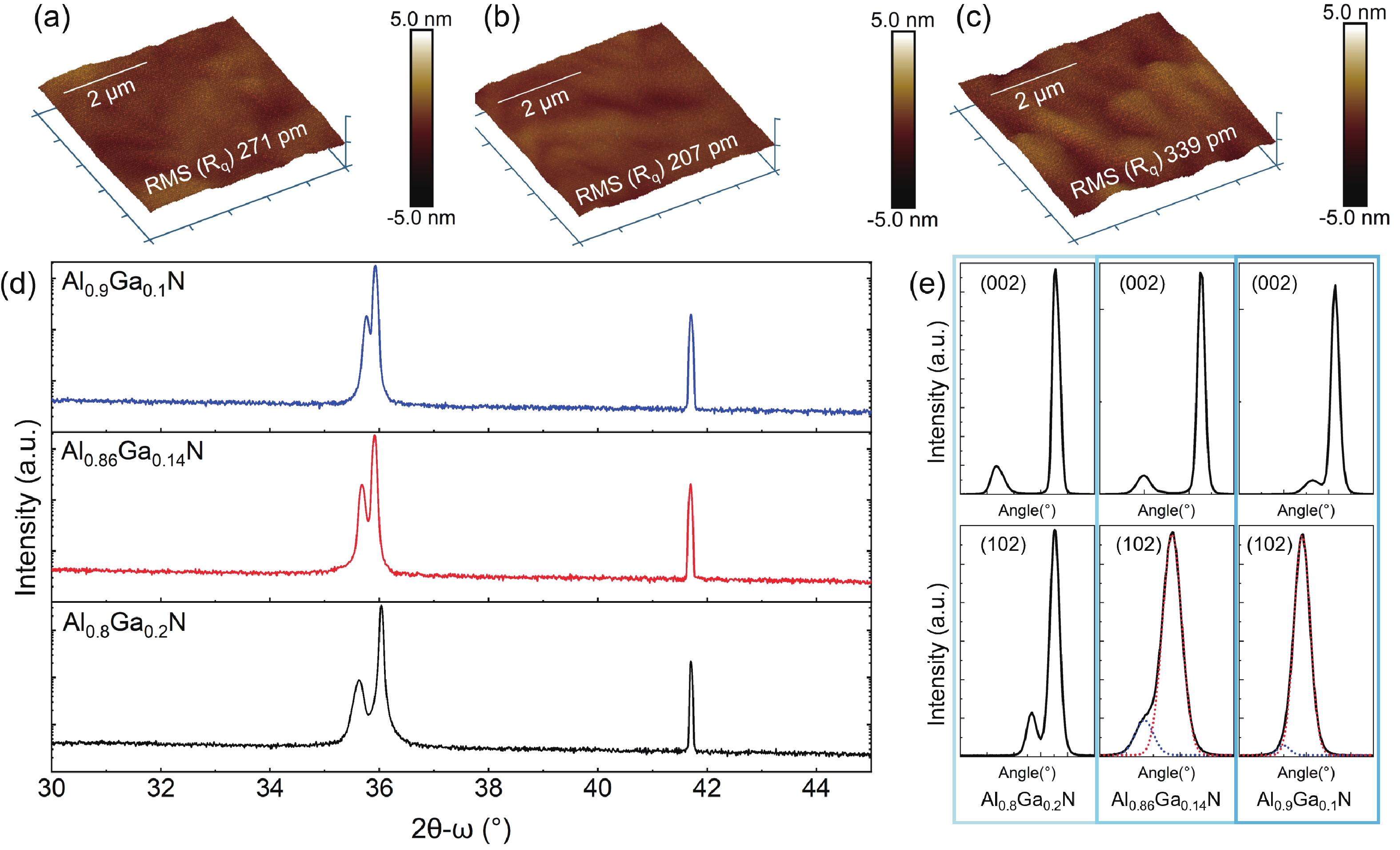
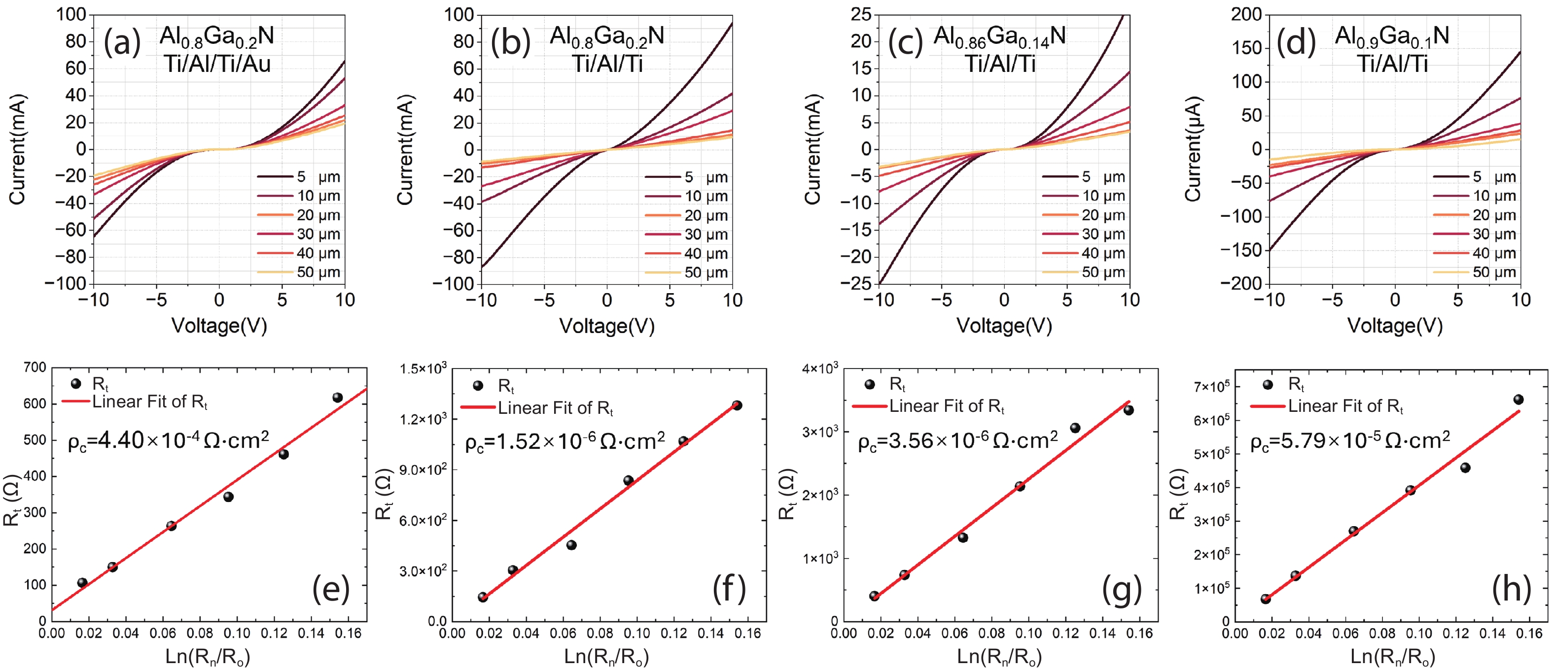
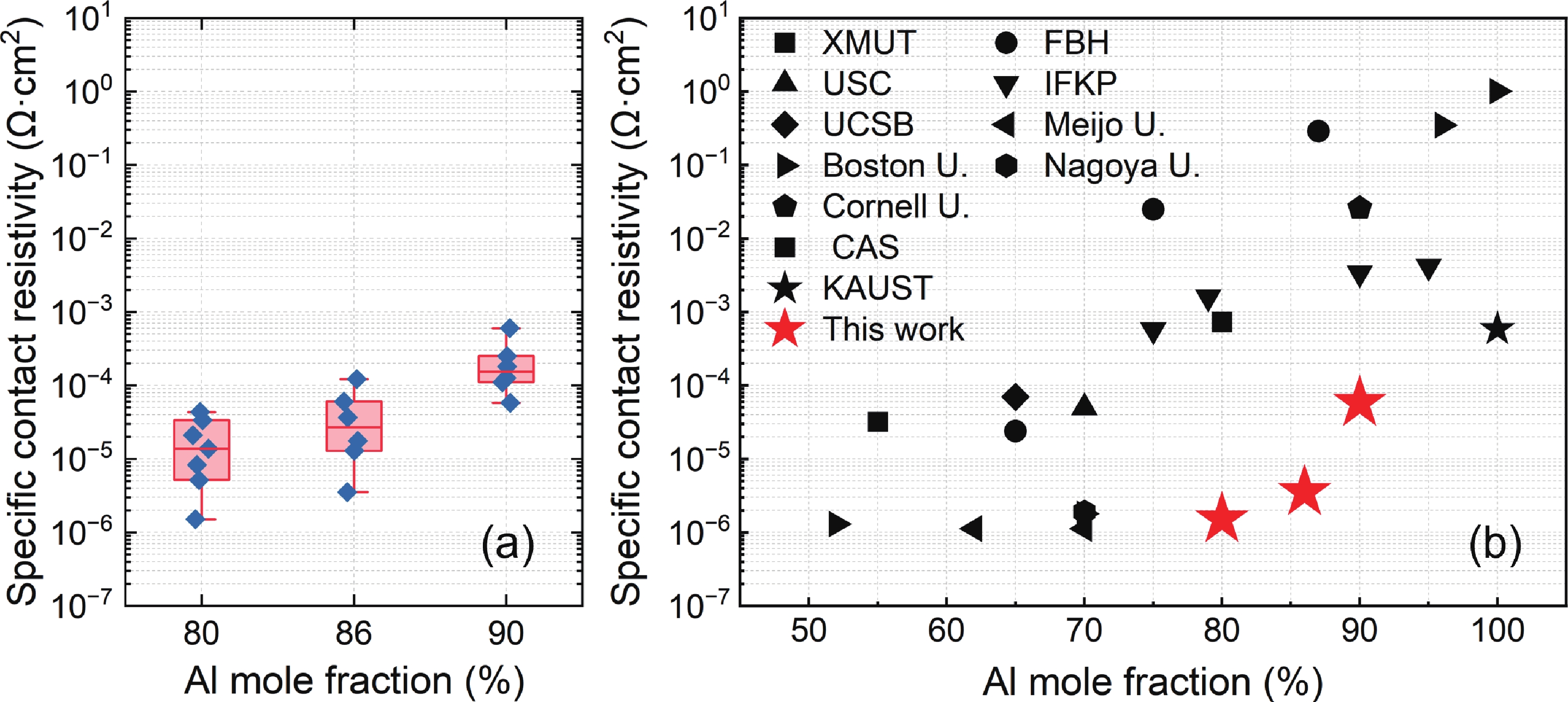
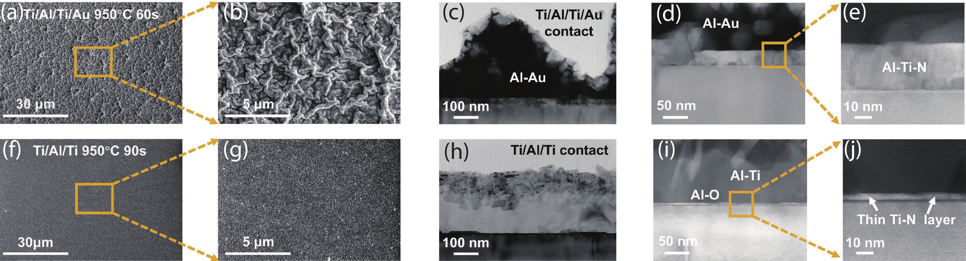
| [1] |
Baca A G, Armstrong A M, Klein B A, et al. Al-rich AlGaN based transistors. J Vac Sci Technol A Vac Surf Films, 2020, 38(2): 020803 doi: 10.1116/1.5129803 |
| [2] |
Hirayama H, Fujikawa S, Kamata N. Recent progress in AlGaN-based deep-UV LEDs. Elect Comm Japan, 2015, 98(5): 1 doi: 10.1364/soled.2014.dw2c.1 |
| [3] |
Zhang Y N, Zhang J C, Liu Z H, et al. Demonstration of a 2 kV Al 0.85Ga 0.15N Schottky barrier diode with improved on-current and ideality factor. IEEE Electron Device Lett, 2020, 41(3): 457 doi: 10.1109/LED.2020.2967895 |
| [4] |
Baca A G, Armstrong A M, Allerman A A, et al. An AlN/Al 0.85Ga 0.15N high electron mobility transistor. Appl Phys Lett, 2016, 109(3): 033509 doi: 10.1063/1.4959179 |
| [5] |
Douglas E A, Reza S, Sanchez C, et al. Ohmic contacts to Al-rich AlGaN heterostructures. Phys Status Solidi A, 2017, 214(8): 1600842 doi: 10.1002/pssa.201600842 |
| [6] |
Peng J L, Jiang K, Zhang S L, et al. Reducing specific contact resistivity of V/Al/Ti/Au n-electrode on n-AlGaN with Al content over 80% for far-UVC LEDs. J Semicond, 2025, 46(9): 092501 doi: 10.1088/1674-4926/25010026 |
| [7] |
Readinger E D, Mohney S E, Pribicko T G, et al. Ohmic contacts to Al-rich n-AlGaN. Electron Lett, 2002, 38(20): 1230 doi: 10.1049/el:20020800 |
| [8] |
Cao H C, Nong M T, Li J Q, et al. Low contact resistivity at the 10 –4 Ω cm 2 level fabricated directly on n-type AlN. Appl Phys Lett, 2024, 125(8): 081602 doi: 10.1063/5.0215744 |
| [9] |
Razzak T, Hwang S, Coleman A, et al. Design of compositionally graded contact layers for MOCVD grown high Al-content AlGaN transistors. Appl Phys Lett, 2019, 115(4): 043502 doi: 10.1063/1.5108529 |
| [10] |
Cho H K, Mogilatenko A, Susilo N, et al. Electrical properties and microstructure of V/Al/Ni/Au contacts on n-Al 0.65Ga 0.35N: Si with different Au thicknesses and annealing temperatures. Semicond Sci Technol, 2022, 37(10): 105016 doi: 10.1088/1361-6641/ac8e8f |
| [11] |
Sulmoni L, Mehnke F, Mogilatenko A, et al. Electrical properties and microstructure formation of V/Al-based n-contacts on high Al mole fraction n-AlGaN layers. Photon Res, 2020, 8(8): 1381 doi: 10.1364/PRJ.391075 |
| [12] |
Chettri D, Mainali G, Cao H C, et al. Demonstration of aluminum nitride metal oxide semiconductor field effect transistor on sapphire substrate. J Phys D: Appl Phys, 2025, 58(3): 035104 doi: 10.1088/1361-6463/ad8759 |
| [13] |
Miller M A, Lin S K, Mohney S E. V/Al/V/Ag contacts to n-GaN and n-AlGaN. J Appl Phys, 2008, 104(6): 064508 doi: 10.1063/1.2980038 |
| [14] |
Nagata N, Senga T, Iwaya M, et al. Reduction of contact resistance in V-based electrode for high AlN molar fraction n-type AlGaN by using thin SiN x intermediate layer. Phys Status Solidi C, 2017, 14(8): 1600243 doi: 10.1002/pssc.201600243 |
| [15] |
Nong M T, Liao C H, Tang X, et al. Epitaxial AlN film with improved quality on Si (111) substrates realized by boron pretreatment via MOCVD. Appl Phys Lett, 2024, 124(17): 172107 doi: 10.1063/5.0207884 |
| [16] |
Sarkar B, Washiyama S, Breckenridge M H, et al. N- and P- type doping in Al-rich AlGaN and AlN. ECS Trans, 2018, 86(12): 25
|
| [17] |
Wang J M, Xu F J, Zhang L S, et al. Progress in efficient doping of Al-rich AlGaN. J Semicond, 2024, 45(2): 021501 doi: 10.1088/1674-4926/45/2/021501 |
| [18] |
Chua E K, Zhao R, Shi L P, et al. Effect of metals and annealing on specific contact resistivity of GeTe/metal contacts. Appl Phys Lett, 2012, 101: 012107 doi: 10.1063/1.4732787 |
| [19] |
Herath Mudiyanselage D, Wang D W, Da B C, et al. Over 600 V lateral AlN-on-AlN Schottky barrier diodes with ultra-low ideality factor. Appl Phys Express, 2024, 17(7): 074001 doi: 10.35848/1882-0786/ad5e5a |
| [20] |
Maeda T, Page R, Nomoto K, et al. AlN quasi-vertical Schottky barrier diode on AlN bulk substrate using Al 0.9Ga 0.1N current spreading layer. Appl Phys Express, 2022, 15(6): 061007 doi: 10.35848/1882-0786/ac702e |
| [21] |
Cho H K, Ostermay I, Kolbe T, et al. Au-free V/Al/Pt contacts on n-Al 0.85Ga 0.15N: Si surfaces of far-UVC LEDs. ECS J Solid State Sci Technol, 2024, 13(9): 093009 doi: 10.1149/2162-8777/ad78ff |
| [22] |
France R, Xu T, Chen P P, et al. Vanadium-based Ohmic contacts to n-AlGaN in the entire alloy composition. Appl Phys Lett, 2007, 90(6): 062115 doi: 10.1063/1.2458399 |
| [23] |
Ji J L, Liu T, He Z K, et al. Semipolar (11–22) AlN films grown by hydride vapor phase epitaxy for Schottky barrier diodes. Cryst Growth Des, 2024, 24(9): 3960 doi: 10.1021/acs.cgd.4c00292 |
| [24] |
Yang Y, Xiong F B, Lin H Y, et al. Evaluation of Ti/Al/Ni/Au ohmic contact to n-AlGaN with different Ti/Al thickness for deep ultraviolet light emitting diode. Solid State Electron, 2023, 208: 108752 doi: 10.1016/j.sse.2023.108752 |
| [25] |
Cho H K, Rass J, Mogilatenko A, et al. Impact of plasma treatment of n-Al 0.87Ga 0.13N: Si surfaces on V/Al/Ni/Au contacts in far-UVC LEDs. IEEE Photonics Technol Lett, 2023, 35(17): 915 doi: 10.1109/LPT.2023.3288216 |
| [26] |
Zollner C J, Yao Y F, Wang M, et al. Highly conductive n-Al 0.65Ga 0.35N grown by MOCVD using low V/III ratio. Crystals, 2021, 11(8): 1006 doi: 10.3390/cryst11081006 |
| [27] |
Lapeyrade M, Alamé S, Glaab J, et al. Effect of Cl 2 plasma treatment and annealing on vanadium based metal contacts to Si-doped Al 0.75Ga 0.25N. J Appl Phys, 2017, 122(12): 125701 doi: 10.1063/1.4993447 |
| [28] |
Mori K, Takeda K, Kusafuka T, et al. Low-ohmic-contact-resistance V-based electrode for n-type AlGaN with high AlN molar fraction. Jpn J Appl Phys, 2016, 55(5S): 05FL03 doi: 10.7567/JJAP.55.05FL03 |
| [29] |
Srivastava S, Hwang S M, Islam M, et al. Ohmic contact to high-aluminum-content AlGaN epilayers. J Electron Mater, 2009, 38(11): 2348 doi: 10.1007/s11664-009-0924-y |


 Tingang Liu got his bachelor’s degree in 2022 from University of Electronics Science and Technology of China and his master’s degree in 2023 from King Abdullah University of Science and Technology. Now he is a doctoral student at King Abdullah University of Science and Technology under the supervision of Prof. Xiaohang Li. His research focuses on ultra-wide bandgap Al-rich AlGaN based power devices.
 Xiaohang Li received his bachelor’s degree in Applied Physics from Huazhong University of Science and Technology, China, his master's degree in Electrical Engineering from Lehigh University, U.S., and his Ph.D. degree in Electrical Engineering from Georgia Institute of Technology, U.S. Prof. Li has extensive research experience in Ⅲ-nitride and Ⅲ-oxide (ultra)wide bandgap semiconductors.
 DownLoad: