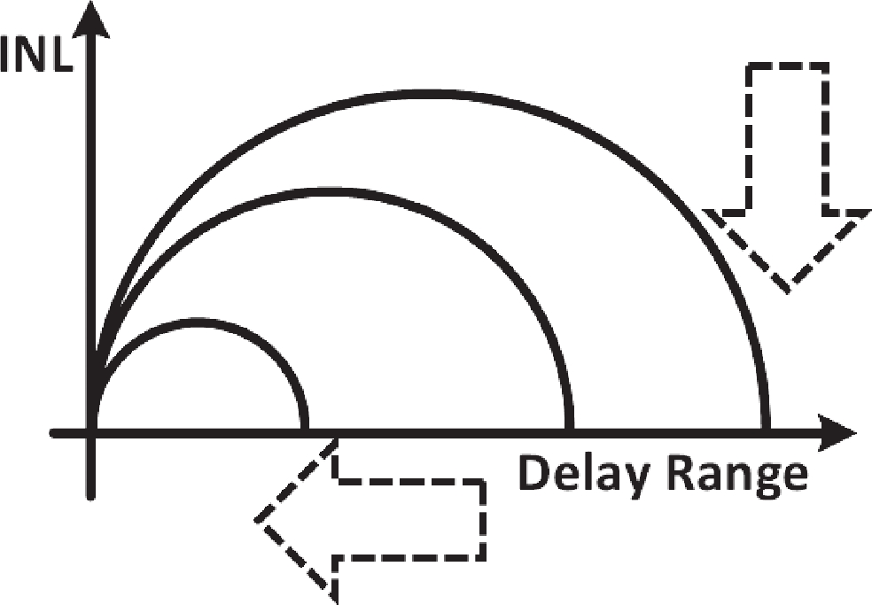
Fig. 1.
The trade-off between DTC INL and its delay range.
FOCUS TOPIC ARTICLES
Yan Chen1, Gaofeng Jin1, Haojie Xu1, Lei Zeng2 and Xiang Gao1,
Corresponding author: Xiang Gao, xiang.gao@zju.edu.cn
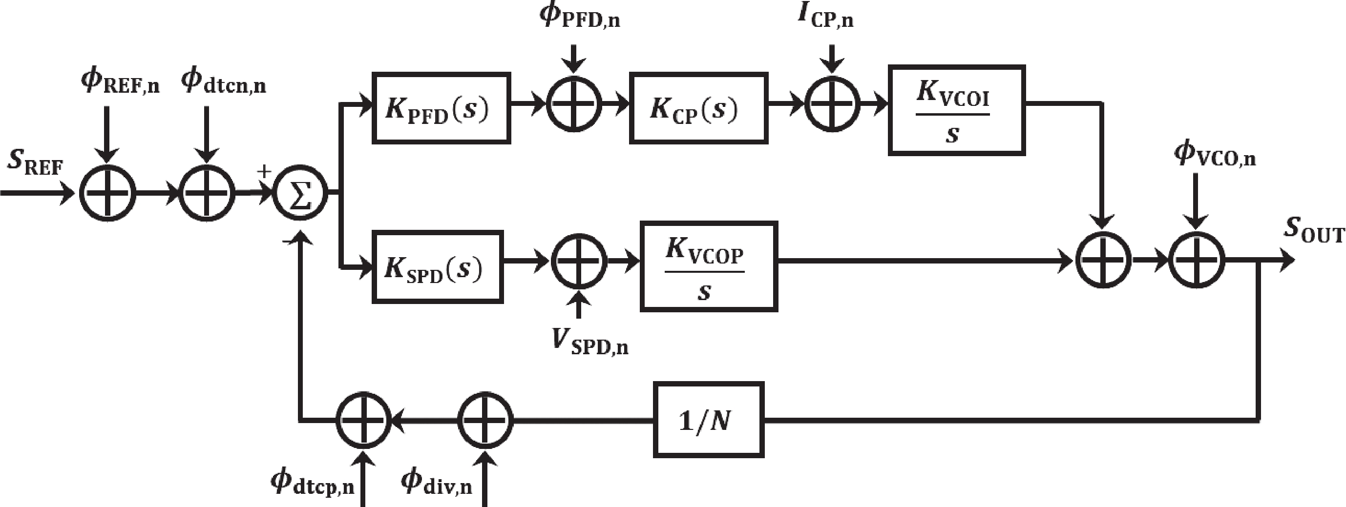
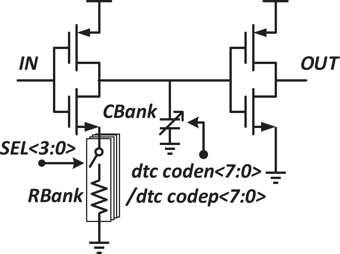
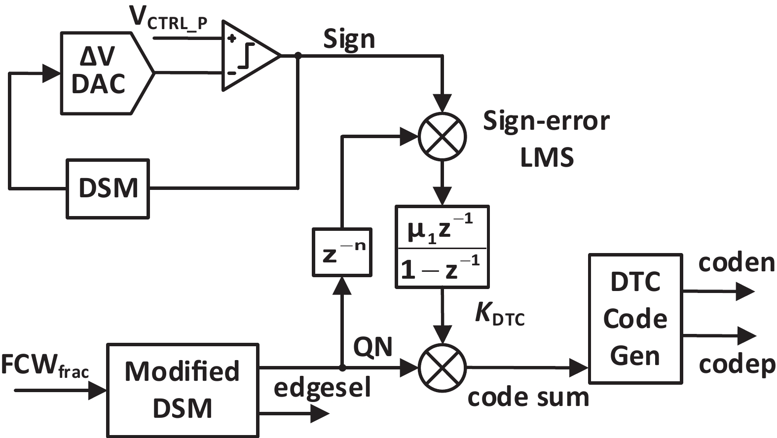
Abstract: In fractional-N phase-locked loops, minimizing the integral nonlinearity (INL) of the digital-to-time converter (DTC) is crucial since it directly limits PLL performance. Considering the trade-off between DTC delay range and linearity, this paper presents a fractional-N dual-path SPD/PFD PLL (DP-SPFDPLL) with a complementary DTC pair. Controlled by the complementary control words, two DTCs are introduced before the two inputs of the phase detector for DTC range reduction and INL cancellation. The required DTC range is further halved by using differential VCO outputs to retime the frequency divider output. The overall design collectively achieves a 4× reduction in DTC range requirement. Fabricated in 7 nm FinFET, the DP-SPFDPLL achieves 118 fs RMS jitter and −247.5 dB figure-of-merit.
Keywords: DP-SPFDPLL, differential DTC, phase selection, MMDIV, DTC range, fractional-N
| [1] |
Gao X, Klumperink E A M, Bohsali M, et al. A low noise sub-sampling PLL in which divider noise is eliminated and PD/CP noise is not multiplied by N2. IEEE J Solid State Circuits, 2009, 44(12): 3253 doi: 10.1109/JSSC.2009.2032723
|
| [2] |
Wu W H, Yao C W, Guo C K, et al. A 14-nm ultra-low jitter fractional-N PLL using a DTC range reduction technique and a reconfigurable dual-core VCO. IEEE J Solid State Circuits, 2021, 56(12): 3756 doi: 10.1109/JSSC.2021.3111134
|
| [3] |
Zhang Z. CMOS analog and mixed-signal phase-locked loops: An overview. J Semicond, 2020, 41(11): 111402 doi: 10.1088/1674-4926/41/11/111402
|
| [4] |
Yin J, Li H R, Lin X Q, et al. Progress and trends of low-jitter fractional-N PLL. J Semicond, 2025, 46(7): 070203 doi: 10.1088/1674-4926/25040035
|
| [5] |
Wu W H, Yao C W, Godbole K, et al. A 28-nm 75-fs rms analog fractional-N sampling PLL with a highly linear DTC incorporating background DTC gain calibration and reference clock duty cycle correction. IEEE J Solid State Circuits, 2019, 54(5): 1254 doi: 10.1109/JSSC.2019.2899726
|
| [6] |
Liu B G, Zhang Y C, Qiu J J, et al. A fully synthesizable fractional-N MDLL with zero-order interpolation-based DTC nonlinearity calibration and two-step hybrid phase offset calibration. IEEE Trans Circuits Syst I Regul Pap, 2021, 68(2): 603 doi: 10.1109/TCSI.2020.3035373
|
| [7] |
Jin G F, Feng F, Chen Y, et al. A low-jitter fractional-N LC-PLL with a 1/4 DTC-range-reduction technique. IEEE Solid State Circuits Lett, 2025, 8: 45. doi: 10.1109/LSSC.2025.3528005
|
| [8] |
Park H, Hwang C, Seong T, et al. A low-jitter ring-DCO-based fractional-N digital PLL with a 1/8 DTC-range-reduction technique using a quadruple-timing-margin phase selector. IEEE J Solid State Circuits, 2022, 57(12): 3527 doi: 10.1109/JSSC.2022.3200475
|
| [9] |
Liu Y C, Wang K H, Li Y, et al. A 37.5fs-rms jitter and –254.1dB FoM fractional-N sampling PLL with reference-phase-selection and complementary-DTC achieving 8× DTC range reduction and zero DTC delay offset. 2025 IEEE Custom Integrated Circuits Conference (CICC), 2025: 1 doi: 10.1109/CICC63670.2025.10983724
|
| [10] |
Xu D X, Liu Z Z, Kuai Y F, et al. 10.3 a 7GHz digital PLL with cascaded fractional divider and pseudo-differential DTC achieving-62.1dBc fractional spur and 143.7fs integrated jitter. 2024 IEEE International Solid-State Circuits Conference (ISSCC), 2024: 192 doi: 10.1109/ISSCC49657.2024.10454284
|
| [11] |
Jin G F, Feng F, Gao X, et al. A 3.3-4.5GHz fractional-N sampling PLL with a merged constant slope DTC and sampling PD in 40nm CMOS. 2021 IEEE Radio Frequency Integrated Circuits Symposium (RFIC), 2021: 63 doi: 10.1109/RFIC51843.2021.9490495
|
| [12] |
Rossoni M, Dartizio S M, Tesolin F, et al. 10.1 an 8.75GHz fractional-N digital PLL with a reverse-concavity variable-slope DTC achieving 57.3fsrms integrated jitter and –252.4dB FoM. 2024 IEEE International Solid-State Circuits Conference (ISSCC), 2024: 188 doi: 10.1109/ISSCC49657.2024.10454388
|
| [13] |
Levantino S, Marzin G, Samori C. An adaptive pre-distortion technique to mitigate the DTC nonlinearity in digital PLLs. IEEE J Solid State Circuits, 2014, 49(8): 1762 doi: 10.1109/JSSC.2014.2314436
|
| [14] |
Liu C X, Staszewski R B, Siriburanon T. Analysis of fractional spurs in a DTC-assisted ADPLL exploiting crystal-oscillator waveform with harmonic-based digital predistortion. IEEE Trans Circuits Syst II Express Briefs, 2025, 72(11): 1560. doi: 10.1109/tcsii.2025.3584351
|
| [15] |
Chen P, Yin J, Zhang F F, et al. Mismatch analysis of DTCs with an improved BIST-TDC in 28-nm CMOS. IEEE Trans Circuits Syst I Regul Pap, 2022, 69(1): 196 doi: 10.1109/TCSI.2021.3105451
|
| [16] |
Hu Y Z, Tao W C, Staszewski R B. Nonlinearity-induced spur analysis in fractional-N synthesizers with ΔΣ quantization cancellation. IEEE Open J Solid State Circuits Soc, 2024, 4: 226 doi: 10.1109/OJSSCS.2024.3476035
|
| [17] |
Chen Y, Jin G F, Xu H J, et al. A dual-path SPD/PFD PLL with PVT-insensitive loop bandwidth. IEEE Solid State Circuits Lett, 2025, 8: 237 doi: 10.1109/LSSC.2025.3589568
|
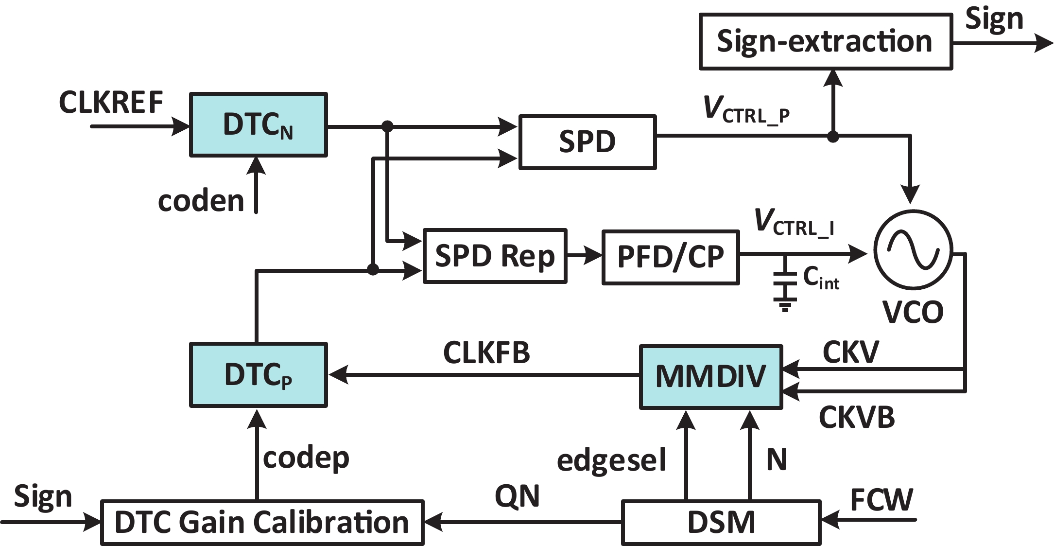
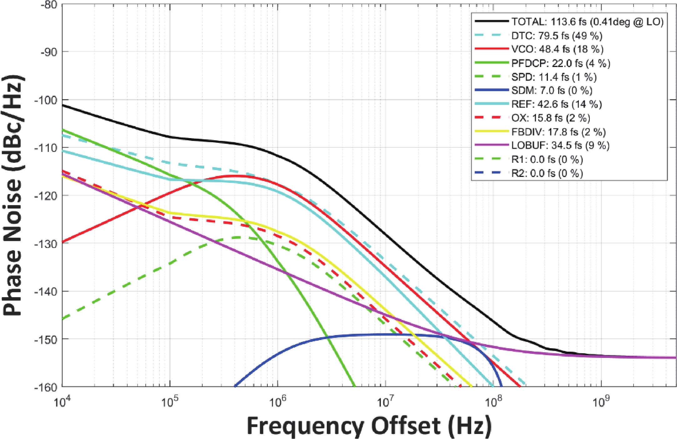
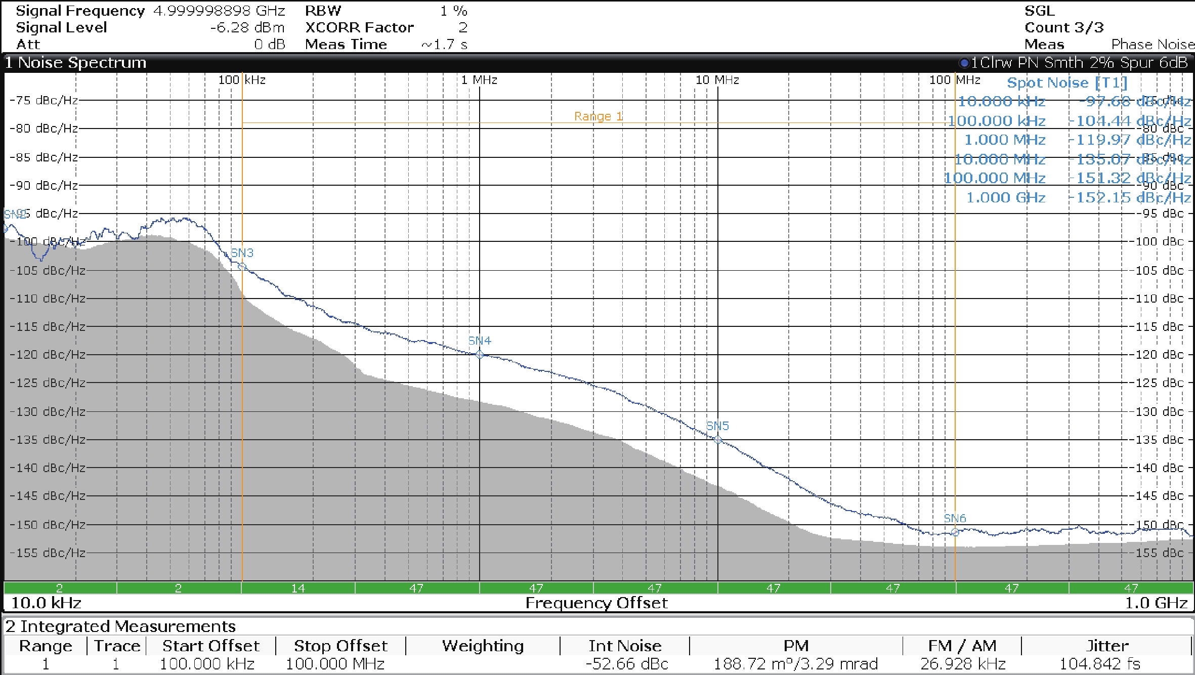
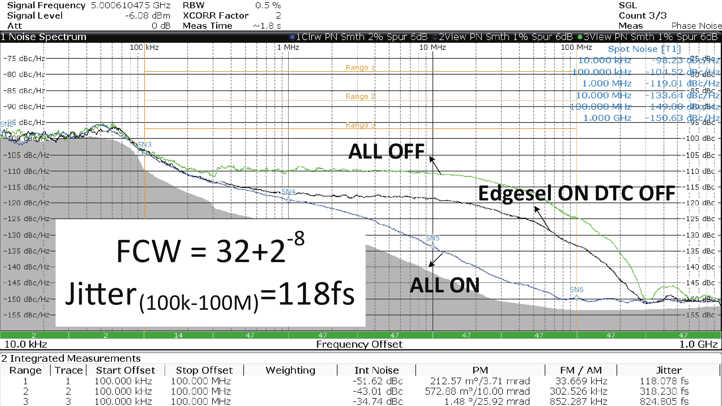

Table 1. Performance summary and comparison.
| Parameter | SSC-L'25[7] | ISSCC'24[10] | ISSCC'24[12] | This work |
| Technology | 40 nm CMOS | 65 nm CMOS | 28 nm CMOS | 7 nm FinFET |
| Reference (MHz) | 100 | 100 | 250 | 312.5 |
| Fout (GHz) | 3.3−4.46 | 6.5−7.5 | 8.75−10.25 | 8.5−14 |
| RMS jitter (fs) | 159.3 | 143.8 | 57.3 | 118 |
| Ref. spur (dBc) | −70 | − | −69.4 | −70 |
| Frac. spur (dBc) | −57 | −62.1 | −63.4 | −40 |
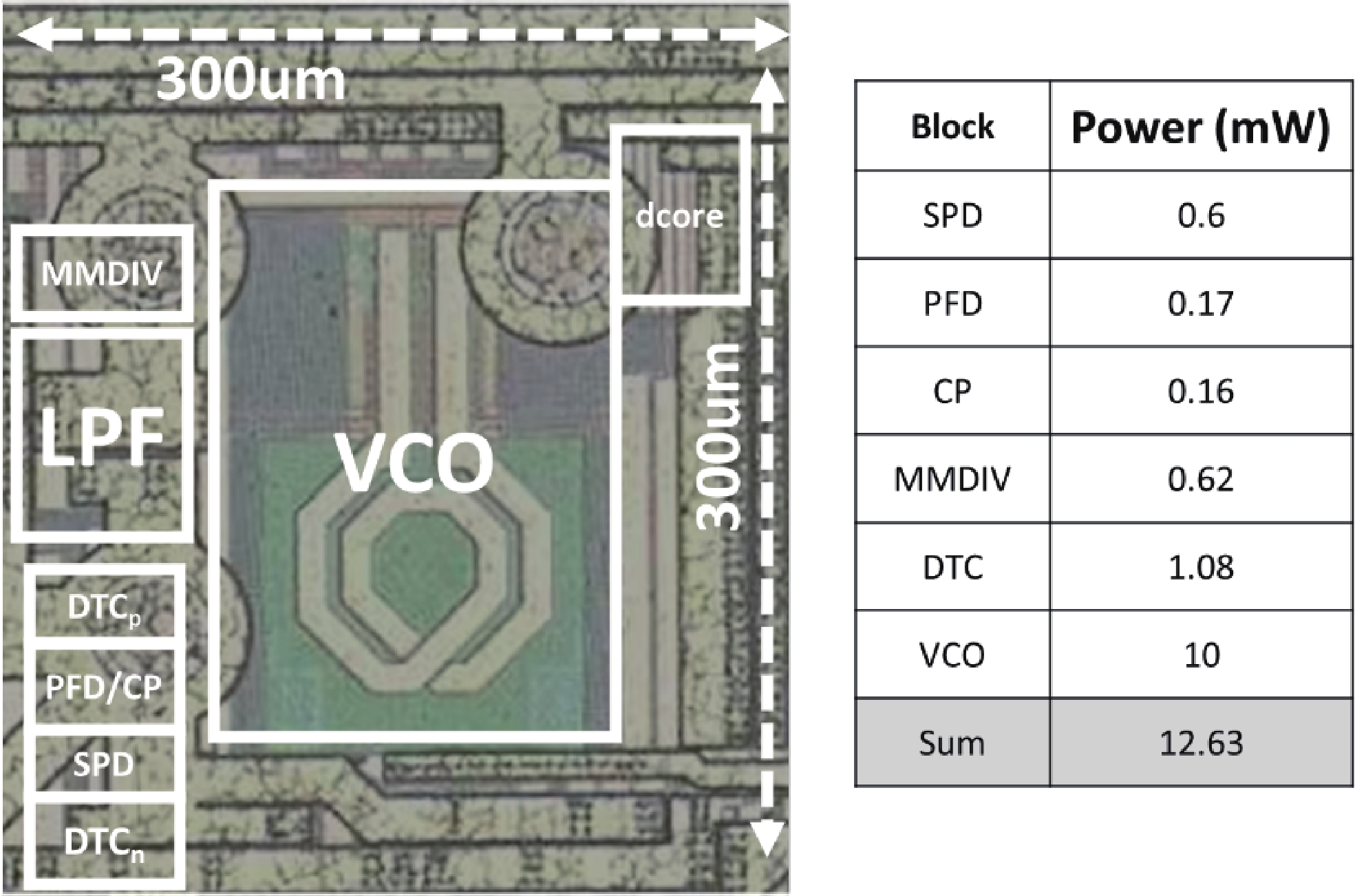
| Power (mW) | 2.6* | 8.89 | 17.5 | 12.63 |
| FoM (dB) | −251.8 | −247.4 | −253.5 | −247.5 |
| Core area (mm2) | 0.36 | 0.23 | 0.21 | 0.09 |
| *Not including reference buffer. | ||||
 DownLoad: CSV
| [1] |
Gao X, Klumperink E A M, Bohsali M, et al. A low noise sub-sampling PLL in which divider noise is eliminated and PD/CP noise is not multiplied by N2. IEEE J Solid State Circuits, 2009, 44(12): 3253 doi: 10.1109/JSSC.2009.2032723
|
| [2] |
Wu W H, Yao C W, Guo C K, et al. A 14-nm ultra-low jitter fractional-N PLL using a DTC range reduction technique and a reconfigurable dual-core VCO. IEEE J Solid State Circuits, 2021, 56(12): 3756 doi: 10.1109/JSSC.2021.3111134
|
| [3] |
Zhang Z. CMOS analog and mixed-signal phase-locked loops: An overview. J Semicond, 2020, 41(11): 111402 doi: 10.1088/1674-4926/41/11/111402
|
| [4] |
Yin J, Li H R, Lin X Q, et al. Progress and trends of low-jitter fractional-N PLL. J Semicond, 2025, 46(7): 070203 doi: 10.1088/1674-4926/25040035
|
| [5] |
Wu W H, Yao C W, Godbole K, et al. A 28-nm 75-fs rms analog fractional-N sampling PLL with a highly linear DTC incorporating background DTC gain calibration and reference clock duty cycle correction. IEEE J Solid State Circuits, 2019, 54(5): 1254 doi: 10.1109/JSSC.2019.2899726
|
| [6] |
Liu B G, Zhang Y C, Qiu J J, et al. A fully synthesizable fractional-N MDLL with zero-order interpolation-based DTC nonlinearity calibration and two-step hybrid phase offset calibration. IEEE Trans Circuits Syst I Regul Pap, 2021, 68(2): 603 doi: 10.1109/TCSI.2020.3035373
|
| [7] |
Jin G F, Feng F, Chen Y, et al. A low-jitter fractional-N LC-PLL with a 1/4 DTC-range-reduction technique. IEEE Solid State Circuits Lett, 2025, 8: 45. doi: 10.1109/LSSC.2025.3528005
|
| [8] |
Park H, Hwang C, Seong T, et al. A low-jitter ring-DCO-based fractional-N digital PLL with a 1/8 DTC-range-reduction technique using a quadruple-timing-margin phase selector. IEEE J Solid State Circuits, 2022, 57(12): 3527 doi: 10.1109/JSSC.2022.3200475
|
| [9] |
Liu Y C, Wang K H, Li Y, et al. A 37.5fs-rms jitter and –254.1dB FoM fractional-N sampling PLL with reference-phase-selection and complementary-DTC achieving 8× DTC range reduction and zero DTC delay offset. 2025 IEEE Custom Integrated Circuits Conference (CICC), 2025: 1 doi: 10.1109/CICC63670.2025.10983724
|
| [10] |
Xu D X, Liu Z Z, Kuai Y F, et al. 10.3 a 7GHz digital PLL with cascaded fractional divider and pseudo-differential DTC achieving-62.1dBc fractional spur and 143.7fs integrated jitter. 2024 IEEE International Solid-State Circuits Conference (ISSCC), 2024: 192 doi: 10.1109/ISSCC49657.2024.10454284
|
| [11] |
Jin G F, Feng F, Gao X, et al. A 3.3-4.5GHz fractional-N sampling PLL with a merged constant slope DTC and sampling PD in 40nm CMOS. 2021 IEEE Radio Frequency Integrated Circuits Symposium (RFIC), 2021: 63 doi: 10.1109/RFIC51843.2021.9490495
|
| [12] |
Rossoni M, Dartizio S M, Tesolin F, et al. 10.1 an 8.75GHz fractional-N digital PLL with a reverse-concavity variable-slope DTC achieving 57.3fsrms integrated jitter and –252.4dB FoM. 2024 IEEE International Solid-State Circuits Conference (ISSCC), 2024: 188 doi: 10.1109/ISSCC49657.2024.10454388
|
| [13] |
Levantino S, Marzin G, Samori C. An adaptive pre-distortion technique to mitigate the DTC nonlinearity in digital PLLs. IEEE J Solid State Circuits, 2014, 49(8): 1762 doi: 10.1109/JSSC.2014.2314436
|
| [14] |
Liu C X, Staszewski R B, Siriburanon T. Analysis of fractional spurs in a DTC-assisted ADPLL exploiting crystal-oscillator waveform with harmonic-based digital predistortion. IEEE Trans Circuits Syst II Express Briefs, 2025, 72(11): 1560. doi: 10.1109/tcsii.2025.3584351
|
| [15] |
Chen P, Yin J, Zhang F F, et al. Mismatch analysis of DTCs with an improved BIST-TDC in 28-nm CMOS. IEEE Trans Circuits Syst I Regul Pap, 2022, 69(1): 196 doi: 10.1109/TCSI.2021.3105451
|
| [16] |
Hu Y Z, Tao W C, Staszewski R B. Nonlinearity-induced spur analysis in fractional-N synthesizers with ΔΣ quantization cancellation. IEEE Open J Solid State Circuits Soc, 2024, 4: 226 doi: 10.1109/OJSSCS.2024.3476035
|
| [17] |
Chen Y, Jin G F, Xu H J, et al. A dual-path SPD/PFD PLL with PVT-insensitive loop bandwidth. IEEE Solid State Circuits Lett, 2025, 8: 237 doi: 10.1109/LSSC.2025.3589568
|


Article views: 741 Times PDF downloads: 119 Times Cited by: 0 Times
Received: 11 December 2025 Revised: 29 January 2026 Online: Accepted Manuscript: 27 February 2026Uncorrected proof: 28 February 2026Published: 11 June 2026
| Citation: |
Yan Chen, Gaofeng Jin, Haojie Xu, Lei Zeng, Xiang Gao. An 8.5−14 GHz fractional-N dual-path SPD/PFD PLL with a complementary DTC pair in 7 nm FinFET[J]. Journal of Semiconductors, 2026, 47(6): 062202. doi: 10.1088/1674-4926/25120023
****
Y Chen, G F Jin, H J Xu, L Zeng, and X Gao, An 8.5−14 GHz fractional-N dual-path SPD/PFD PLL with a complementary DTC pair in 7 nm FinFET[J]. J. Semicond., 2026, 47(6): 062202 doi: 10.1088/1674-4926/25120023

|
 Yan Chen received the B.Eng. degree in microelectronic science and technology from Zhejiang University, Hangzhou, China, in 2021, where she is currently pursuing the Ph.D. degree in electronic science and technology. Her current research interests focus on high-performance frequency synthesizers, clock data recovery circuit design, and mixed-signal circuit design
 Xiang Gao received his Ph.D. degree (cumlaude) from the University of Twente, The Netherlands in 2010. From 2010 to 2016, he was a principal engineer and design manager with Marvell Semiconductor, Santa Clara, CA, focusing on wireless transceivers ICs. From 2016 to 2018, he was an Engineering Director with Credo Semiconductor, Milpitas, CA, working on high-speed SerDes. Since 2018, he is with the Institute of VLSI Design, Zhejiang University, China. He is an IEEE senior member and currently a TPC member of ISSCC and RFIC
| [1] |
Gao X, Klumperink E A M, Bohsali M, et al. A low noise sub-sampling PLL in which divider noise is eliminated and PD/CP noise is not multiplied by N2. IEEE J Solid State Circuits, 2009, 44(12): 3253 doi: 10.1109/JSSC.2009.2032723
|
| [2] |
Wu W H, Yao C W, Guo C K, et al. A 14-nm ultra-low jitter fractional-N PLL using a DTC range reduction technique and a reconfigurable dual-core VCO. IEEE J Solid State Circuits, 2021, 56(12): 3756 doi: 10.1109/JSSC.2021.3111134
|
| [3] |
Zhang Z. CMOS analog and mixed-signal phase-locked loops: An overview. J Semicond, 2020, 41(11): 111402 doi: 10.1088/1674-4926/41/11/111402
|
| [4] |
Yin J, Li H R, Lin X Q, et al. Progress and trends of low-jitter fractional-N PLL. J Semicond, 2025, 46(7): 070203 doi: 10.1088/1674-4926/25040035
|
| [5] |
Wu W H, Yao C W, Godbole K, et al. A 28-nm 75-fs rms analog fractional-N sampling PLL with a highly linear DTC incorporating background DTC gain calibration and reference clock duty cycle correction. IEEE J Solid State Circuits, 2019, 54(5): 1254 doi: 10.1109/JSSC.2019.2899726
|
| [6] |
Liu B G, Zhang Y C, Qiu J J, et al. A fully synthesizable fractional-N MDLL with zero-order interpolation-based DTC nonlinearity calibration and two-step hybrid phase offset calibration. IEEE Trans Circuits Syst I Regul Pap, 2021, 68(2): 603 doi: 10.1109/TCSI.2020.3035373
|
| [7] |
Jin G F, Feng F, Chen Y, et al. A low-jitter fractional-N LC-PLL with a 1/4 DTC-range-reduction technique. IEEE Solid State Circuits Lett, 2025, 8: 45. doi: 10.1109/LSSC.2025.3528005
|
| [8] |
Park H, Hwang C, Seong T, et al. A low-jitter ring-DCO-based fractional-N digital PLL with a 1/8 DTC-range-reduction technique using a quadruple-timing-margin phase selector. IEEE J Solid State Circuits, 2022, 57(12): 3527 doi: 10.1109/JSSC.2022.3200475
|
| [9] |
Liu Y C, Wang K H, Li Y, et al. A 37.5fs-rms jitter and –254.1dB FoM fractional-N sampling PLL with reference-phase-selection and complementary-DTC achieving 8× DTC range reduction and zero DTC delay offset. 2025 IEEE Custom Integrated Circuits Conference (CICC), 2025: 1 doi: 10.1109/CICC63670.2025.10983724
|
| [10] |
Xu D X, Liu Z Z, Kuai Y F, et al. 10.3 a 7GHz digital PLL with cascaded fractional divider and pseudo-differential DTC achieving-62.1dBc fractional spur and 143.7fs integrated jitter. 2024 IEEE International Solid-State Circuits Conference (ISSCC), 2024: 192 doi: 10.1109/ISSCC49657.2024.10454284
|
| [11] |
Jin G F, Feng F, Gao X, et al. A 3.3-4.5GHz fractional-N sampling PLL with a merged constant slope DTC and sampling PD in 40nm CMOS. 2021 IEEE Radio Frequency Integrated Circuits Symposium (RFIC), 2021: 63 doi: 10.1109/RFIC51843.2021.9490495
|
| [12] |
Rossoni M, Dartizio S M, Tesolin F, et al. 10.1 an 8.75GHz fractional-N digital PLL with a reverse-concavity variable-slope DTC achieving 57.3fsrms integrated jitter and –252.4dB FoM. 2024 IEEE International Solid-State Circuits Conference (ISSCC), 2024: 188 doi: 10.1109/ISSCC49657.2024.10454388
|
| [13] |
Levantino S, Marzin G, Samori C. An adaptive pre-distortion technique to mitigate the DTC nonlinearity in digital PLLs. IEEE J Solid State Circuits, 2014, 49(8): 1762 doi: 10.1109/JSSC.2014.2314436
|
| [14] |
Liu C X, Staszewski R B, Siriburanon T. Analysis of fractional spurs in a DTC-assisted ADPLL exploiting crystal-oscillator waveform with harmonic-based digital predistortion. IEEE Trans Circuits Syst II Express Briefs, 2025, 72(11): 1560. doi: 10.1109/tcsii.2025.3584351
|
| [15] |
Chen P, Yin J, Zhang F F, et al. Mismatch analysis of DTCs with an improved BIST-TDC in 28-nm CMOS. IEEE Trans Circuits Syst I Regul Pap, 2022, 69(1): 196 doi: 10.1109/TCSI.2021.3105451
|
| [16] |
Hu Y Z, Tao W C, Staszewski R B. Nonlinearity-induced spur analysis in fractional-N synthesizers with ΔΣ quantization cancellation. IEEE Open J Solid State Circuits Soc, 2024, 4: 226 doi: 10.1109/OJSSCS.2024.3476035
|
| [17] |
Chen Y, Jin G F, Xu H J, et al. A dual-path SPD/PFD PLL with PVT-insensitive loop bandwidth. IEEE Solid State Circuits Lett, 2025, 8: 237 doi: 10.1109/LSSC.2025.3589568
|

 WeChat ID
Journal of Semiconductors © 2017 All Rights Reserved 京ICP备05085259号-2